EUROPEAN ORGANIZATION FOR NUCLEAR RESEARCH (CERN)
![[Uncaptioned image]](/html/1509.02387/assets/x1.png) LHCb-PUB-2016-002
LHCb-PUB-2016-002
Characterisation of Medipix3
Silicon Detectors in a Charged-Particle Beam
K. Akiba1,
J. Alozy2,
R. Aoude3,
M. van Beuzekom4,
J. Buytaert2,
P. Collins2,
A. Dosil Suárez5,
R. Dumps2,
A. Gallas5,
C. Hombach6,
D. Hynds7,
M. John8,
A. Leflat9,
Y. Li10,
E. Pérez Trigo5,
R. Plackett11,
M. M. Reid12,
P. Rodríguez Pérez6,
H. Schindler2†††Corresponding author.,
P. Tsopelas4,
C. Vázquez Sierra5‡‡‡Corresponding author.,
J. J. Velthuis13,
M. Wysokiński14
1 Universidade Federal do Rio de Janeiro, Rio de Janeiro, Brazil
2 European Organization for Nuclear Research (CERN), Geneva, Switzerland
3 Pontifícia Universidade Católica do Rio de Janeiro, Rio de Janeiro, Brazil
4 Nikhef National Institute for Subatomic Physics, Amsterdam, The Netherlands
5 Universidade de Santiago de Compostela, Santiago de Compostela, Spain
6 School of Physics and Astronomy, University of Manchester, Manchester, United Kingdom
7 School of Physics and Astronomy, University of Glasgow, Glasgow, United Kingdom
8 Department of Physics, University of Oxford, Oxford, United Kingdom
9 Institute of Nuclear Physics, Moscow State University (SINP MSU), Moscow, Russia
10 Center for High Energy Physics, Tsinghua University, Beijing, China
11 Diamond Light Source Ltd., Didcot, United Kingdom
12 Department of Physics, University of Warwick, Coventry, United Kingdom
13 H.H. Wills Physics Laboratory, University of Bristol, Bristol, United Kingdom
14 AGH - University of Science and Technology, Faculty of Computer Science, Electronics and Telecommunications, Kraków, Poland
While designed primarily for X-ray imaging applications, the Medipix3 ASIC can also be used for charged-particle tracking. In this work, results from a beam test at the CERN SPS with irradiated and non-irradiated sensors are presented and shown to be in agreement with simulation, demonstrating the suitability of the Medipix3 ASIC as a tool for characterising pixel sensors.
Published in JINST
© CERN on behalf of the LHCb collaboration, licence CC-BY-4.0.
1 Introduction
As part of the upgrade of the LHCb experiment, scheduled for the second long shutdown of the LHC in 2018/19, the present microstrip-based Vertex Locator (VELO) is foreseen to be replaced by a silicon hybrid pixel detector [1] with an ASIC dubbed “VeloPix” which will be derived from the Medipix family of ASICs. Like its predecessors Medipix2, Timepix, Medipix3, and Timepix3, the VeloPix chip will feature a matrix of square pixels with a pitch of 55 m. Prior to the arrival of the Timepix3 ASIC, Timepix and Medipix3 were the most suitable devices for the qualification of prototype sensors for the VELO upgrade. Until the end of lifetime of the upgraded experiment, the pixels closest to the beam line ( mm) accumulate a fluence of up to 1 MeV n cm-2. Qualifying silicon sensors in terms of radiation hardness is therefore a key element of the VELO upgrade R&D programme.
Timepix silicon detectors have been characterised extensively in terms of charged-particle tracking performance [2]. Since the ASIC has per-pixel information on the collected charge in terms of a time-over-threshold (ToT) value, a direct measurement of the charge deposition spectrum is possible.
Medipix3 [3, 4] on the other hand is a pure counting chip which was designed primarily for photon imaging applications. In order to measure the deposited charge in the sensor one therefore has to resort to indirect methods (Section 3). Among the large-scale ASICs in the high-energy physics community, Medipix3 has been the first to be based on IBM 130 nm CMOS technology. Compared to the Timepix (which was fabricated in 250 nm technology), it is expected to be more radiation tolerant [5] and thus lends itself for testing irradiated sensors.
In this work, we report on measurements with irradiated and non-irradiated Medipix3 assemblies carried out in 2012 at the H8 beamline of the CERN North Area facility, using positively charged hadrons with a momentum of 180 GeV/. These measurements are intended to provide a validation of the chip functionality and performance complementary to characterisation measurements using photon sources. In addition, they also represent a first step towards a comprehensive evaluation of the radiation hardness of silicon pixel sensors with the “Medipix footprint” of m2 pixels.
2 Setup
The Timepix telescope, described in Ref. [6], was used for reconstructing the tracks of particles crossing the Medipix3 device under test (DUT). In order to minimise the pointing error, the DUT was placed in the centre of the telescope. For reading out the Medipix3 chip, the “Merlin” data acquisition system [7] developed at the Diamond Light Source facility was used. The synchronisation of Timepix and Medipix3 is straightforward, as both ASICs work in a “camera-style” frame-based readout mode. An external circuit implemented using NIM modules was used for sending shutter opening and closing signals to the telescope and the device under test. The coincident firing of two scintillators located upstream and downstream of the telescope was used for counting the number of beam particles traversing the telescope and the duration of a shutter was adjusted such that 50 scintillator triggers were accumulated in one frame. During one spill (9.6 s) typically about 500 frames were recorded.
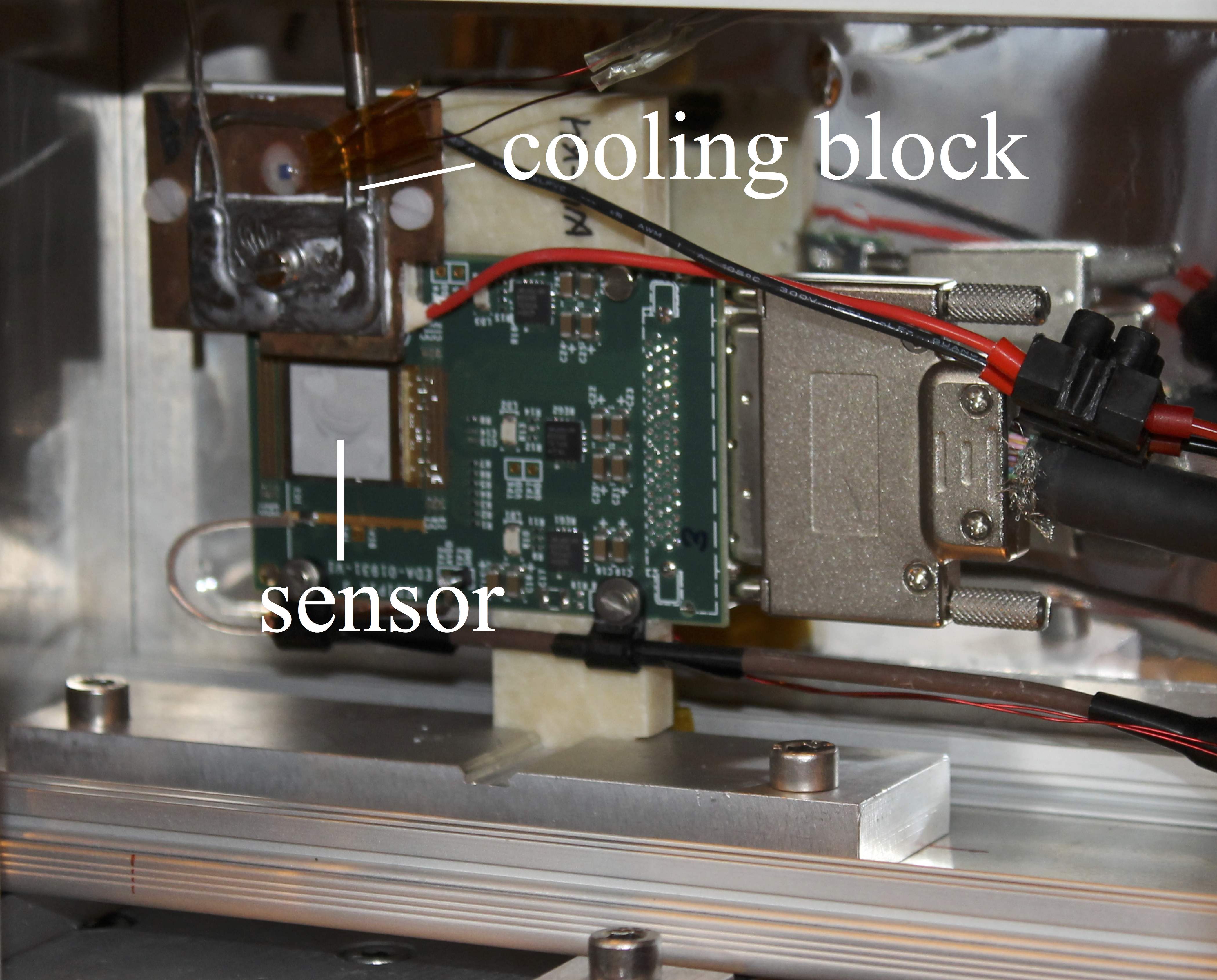
The temperature of the irradiated samples was controlled using a combination of thermoelectric and CO2 cooling, the latter being provided by a portable cooling plant [8]. As can be seen on the photograph in figure 1, the chip was glued onto a tape of Thermal Pyrolytic Graphite (TPG) the other end of which was attached to the cold side of a Peltier cooler. The hot side of the Peltier cooler was put in contact with an aluminium cooling block through which CO2 was circulating. With the chip switched off, a temperature of approximately C was reached, rising to C with the chip in operation. The setup was placed in a light-tight aluminium case which was flushed with nitrogen. The non-irradiated assemblies were measured at room temperature.
In all measurements discussed below, the DUTs were -on- silicon sensors bump-bonded to Medipix3.1 ASICs. The ASICs were operated in single-pixel high-gain mode and only one threshold (DAC THL) was used. Before taking data, a threshold equalisation was performed using the front-end noise as reference. The equalisation procedure consists of optimising the DAC values of two global current sources (ThresholdN and DACpixel) and the threshold adjustment bits of each pixel, such that the THL value corresponding to the noise floor lies within a certain window for all pixels. For the non-irradiated assemblies a target window of was used.
Prior to the beam test, calibration measurements using testpulses were performed to determine the relation between THL DAC and injected charge. To verify the viability of the testpulse method, data were taken with a 241Am source for the two non-irradiated assemblies discussed below, and – after applying the calibrations obtained from the testpulse scan – the signal peaks were found to match within 2% between the two assemblies. These measurements were however made with a different readout system [9] and equalisation mask than used in the testbeam (at that time the testpulse functionality was not yet implemented in Merlin).
Where possible111One of the assemblies (W20_B6) was accidentally damaged after the beam test., calibration measurements using test pulses were later (after the beam test) made also using the Merlin system. These calibration curves are used in the following for a relative comparison of the signals measured with different sensors.
3 Measurements
For each track reconstructed in the telescope, the intercept with the DUT plane is calculated. In order to suppress fake tracks a requirement on the track quality is applied and the tracks are required to include hits on all telescope planes. If an unused cluster with a centre of gravity within a radius m around the track intercept is found, it is associated to the track and tagged as used. In case of multiple candidate clusters, the closest one is selected. The hit efficiency (or cluster finding efficiency) is then given by the fraction of tracks with an associated cluster on the DUT. The pointing resolution of the telescope ( m in the present configuration) allows one to probe the hit efficiency as function of the track intercept within a pixel cell. In the analysis we divide the pixel cell in bins and calculate separate efficiencies for each bin.
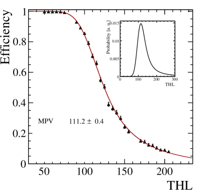
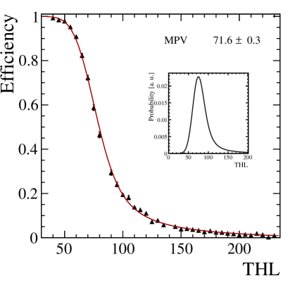
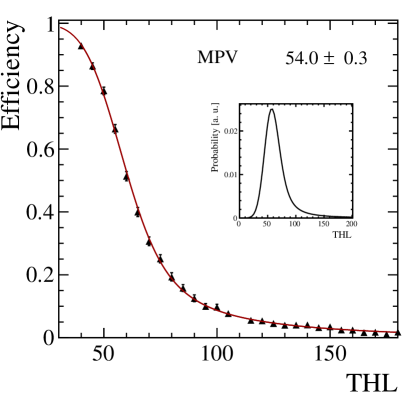
The most probable value (MPV) of the deposited charge can be estimated by scanning the hit efficiency as function of threshold. Assuming that the distribution of the collected charge can be described by a Landau distribution convoluted with a Gaussian distribution , the hit efficiency as a function of the threshold is given by
| (1) |
By fitting the measured efficiency with Eq. (1), the MPV and width of the Landau distribution and the of the Gaussian can be determined (the mean of the Gaussian is fixed to zero). This method requires that the entire charge deposited by a track is collected by a single pixel. We therefore use the hit efficiency in the central bin of the matrix for this measurement.
To determine the spatial resolution, the distributions of the residuals between the coordinates of the track intercepts and the associated clusters are calculated. The standard deviation of the residual distribution is used as a resolution metric (the pointing error of the telescope represents only a small correction when subtracted in quadrature).
4 Results
4.1 Non-irradiated assemblies
The measurements before irradiation were carried out using -on- active-edge sensors with a nominal thickness of 100 m manufactured by VTT222VTT Technical Research Centre of Finland, Espoo, Finland. The MPV of the charge deposition spectrum is thus expected to be around electrons.
Two assemblies, W20_B6 and W20_J9, were tested with beam. After the beam test, part of the backside metallisation was removed from the sensor on W20_B6, and by injecting laser pulses the depletion voltage was determined to be approximately V. In the beam test, both sensors were operated at a bias voltage of V, and were oriented perpendicularly to the beam. For each point in the threshold scan, a data set comprising typically reconstructed telescope tracks was recorded.
From the hit efficiency in the centre of the pixel cell as function of threshold (figure 2), the most probable value of the charge deposition spectrum is determined to correspond to THL for assembly W20_B6 and THL for assembly W20_J9. The statistical errors of the fit values are given in figure 2. Uncertainties due to tracking cuts, alignment, non-linearity of the THL DAC give rise to a systematic error on the MPV of . The MPVs in terms of THL DAC values differ significantly between the two devices. This can be attributed to non-optimised settings of the DAC “Vcas” (for voltage cascode), which sets the reference voltage for some transistors in the pixel circuit and, if not tuned properly, can have an impact on the operating point of the circuit.
As discussed in section 2, testpulse calibration measurements using the Merlin readout system could only be made for assembly W20_J9. To facilitate the comparison between the devices, the results discussed below are therefore presented as function of the threshold-to-signal ratio, i. e. the applied THL DAC normalised to the respective MPV.
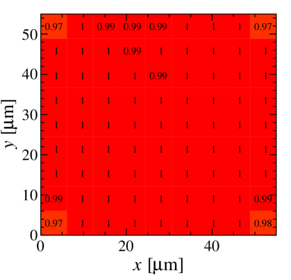
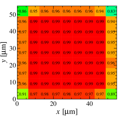
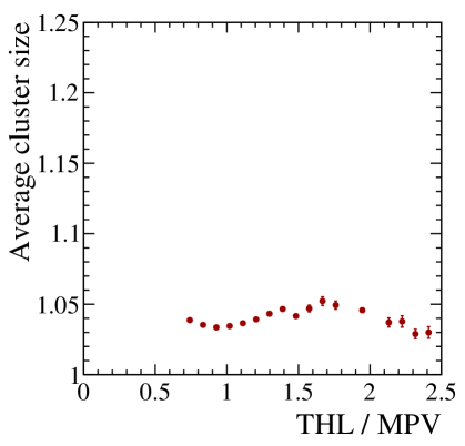
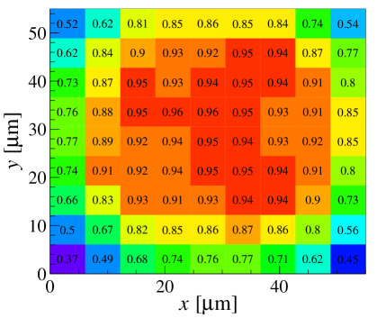
Figure 3 (left) shows the hit efficiency as function of the track intercept within a pixel cell for the lowest threshold-to-signal ratio (THL/MPV) covered by the threshold scan. At this threshold – which is high compared to a typical operational threshold of 1000 electrons – the detector can be seen to be fully efficient (), except at the corners. With increasing threshold – as illustrated in figure 3 (right) – a drop in efficiency becomes noticeable at the borders of the pixel cell. This is a consequence of charge sharing due to diffusion, as can be seen from figure 4 which shows the average cluster size as function of the track intercept within the pixel cell.
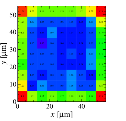
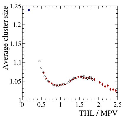
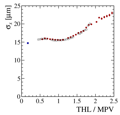
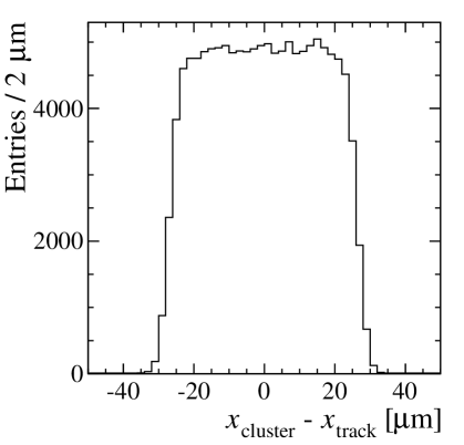
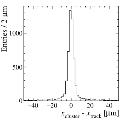
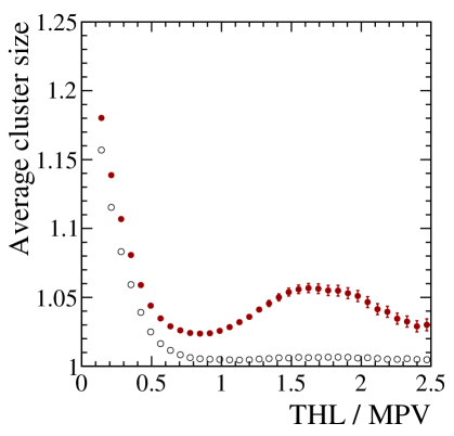
Figure 5 (left) shows the average cluster size as function THL/MPV. At the lowest threshold, an average cluster size of is found, with single-pixel clusters constituting and two-pixel clusters of all associated clusters. The cluster size as function of threshold/signal follows the same shape for both sensors, exhibiting a minimum around THL/MPV and a subsequent maximum around THL/MPV. With increasing threshold, an increasing fraction of the observed clusters is produced by primary particles which suffer collisions with large energy loss. These collisions give rise to energetic electrons which further ionise along their path and produce electron-hole pairs away from the trajectory of the primary particle.
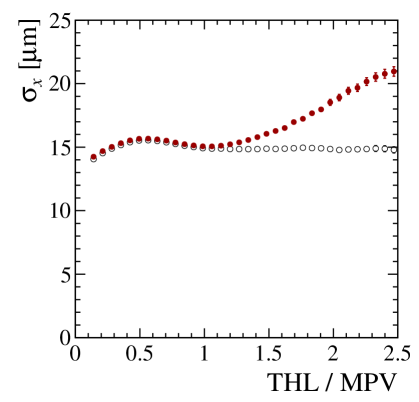
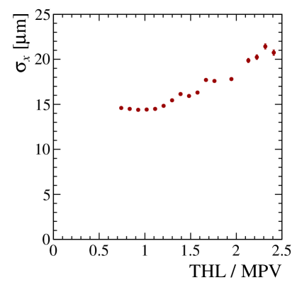
The residual distributions (in the direction) at low threshold for one-pixel and two-pixel clusters are shown in figure 6. Averaged over all cluster sizes, the standard deviation of the residual distribution is found to be m in both and . As expected from the dominance of one-pixel clusters, this value is close to the binary limit ( m m). Figure 5 (right) shows the of the residual distribution in as function of threshold/signal. The resolution can be seen to deteriorate significantly after the threshold crosses the MPV.
Figure 5 also includes results obtained with a Timepix ASIC bump-bonded to a 100 m thick -on- sensor from the same batch. The Timepix assembly was measured in the same beam test campaign and was operated at a threshold of 1000 electrons and a bias voltage of V. The data were taken in ToT mode, but the values shown in figure 5 were calculated with the ToT values set to one to mimic the Medipix3 behaviour. The results for the Timepix assembly are in agreement with the extrapolated results from the Medipix3 assemblies.
To understand better the observed shapes of resolution and cluster size as function of threshold, a simple simulation using the Garfield++ toolkit [10] was used. The primary ionisation process is calculated using the Heed program [11], which in addition to the energy loss by the traversing charged particle also simulates the ionisation cascade from high-energy (“delta”) electrons produced in the interactions of the charged particle with the silicon medium as well as the spatial distribution of the resulting electron-hole pairs. Each electron is subsequently transported through the sensor, based on the drift velocity and diffusion coefficient as function of the electric field. A one-dimensional approximation for the electric field is used333The electric field is assumed to vary linearly between at the sensor backside and at the implants, where is the sensor thickness..
As can be seen from figure 7, the features in the measured cluster size and resolution as function of threshold-to-signal ratio are reproduced by the simulation, provided that the spatial extent of the ionisation pattern is taken into account. This corroborates the conclusion that these features are due to “delta” electrons.
4.2 Irradiated assemblies
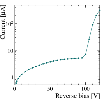
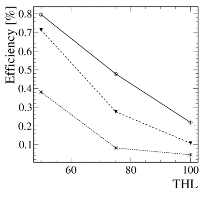
A set of Medipix3.1 assemblies, with VTT -on- active-edge sensors from the same batch as the non-irradiated sensors discussed above, were irradiated at the Ljubljana TRIGA reactor [12] to a 1 MeV neutron equivalent fluence of cm-2 and subsequently annealed for 80 minutes at C. From lab measurements with a laser, the effective depletion voltage of these sensors after irradiation was measured to be between and V. One of the assemblies, W20_H5, was characterised in the beam test. The sensor, which has a pixel-to-edge distance of 100 m, was operated at a bias voltage of V as operation at higher bias was inhibited by the onset of electrical breakdown (figure 8).
In general, the irradiated assemblies exhibited a higher dark count rate compared to the non-irradiated ones, which was attributed to electrons from the -decay of 182Ta produced by neutron activation during the irradiation of the ASIC444 The presence of 182Ta in the irradiated assemblies was confirmed by gamma spectroscopy measurements performed by the CERN radioprotection group.. This – presumably in combination with other radiation effects – resulted in problems during the equalisation procedure for some assemblies, as well as a larger threshold dispersion. The optimised values of the DACs which control the global currents (ThresholdN and DACpixel) were larger (by a factor 2 – 3) compared to the non-irradiated assemblies.
As can be seen from figure 9, the MPV of the charge deposition spectrum corresponds to a THL DAC of . After correcting for the differences in gain and offset using testpulse calibration curves, this value is found to be approximately 8.5% lower than the MPV of the non-irradiated sensors.
As in the non-irradiated case, the cluster size spectrum is dominated by single-pixel clusters. Cluster size and of the -residual distribution as function of threshold-to-signal ratio (figure 10) follow closely the corresponding curves for the non-irradiated assemblies (figure 5).
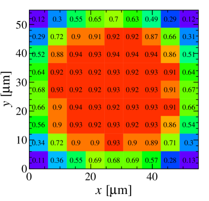
Figure 11 shows the hit efficiency as function of the track intercept within a pixel cell at the lowest measured threshold (). In the centre of the pixel cell, an efficiency of is found, compared to for the non-irradiated assemblies at the same threshold-to-signal ratio ().
A further beam test measurement was performed with a Medipix3.1 ASIC bump-bonded to a 200 m thick -on- sensor manufactured by CNM555Centro Nacional de Microelectrónica, Barcelona, Spain. The sensor featured two guard rings and was diced at a distance of 400 m from the border of the pixel matrix. The assembly (W20_D6) was also irradiated at Ljubljana, but to a higher fluence, 1 MeV n cm-2. During the equalisation procedure, a large threshold dispersion was observed, such that the upper limit of the equalisation target window needed to be increased to . In addition, a significant fraction () of the pixels needed to be masked. Tracks crossing a masked pixel were thus excluded from the efficiency measurements for this device.
Because of time constraints, data were taken only at three THL values with this device, such that determining the MPV of the charge deposit spectrum was not possible.
Figure 12 shows the efficiency as function of the track intercept. The dependency of the efficiency on the applied threshold and bias voltage is shown in figure 13.
5 Conclusions
First results on the performance of hadron-irradiated pixel detectors with the “footprint” of the upgraded LHCb VELO ( m2 pixels) have been obtained from a beam test at the CERN SPS, using Medipix3.1 ASICs bump-bonded to thin -on- silicon sensors. As the Medipix3 ASICs do not provide a direct measurement of the collected charge, threshold scans were used for characterising the sensor.
Reference measurements with non-irradiated Medipix3.1 assemblies were made in the same testbeam campaign. The threshold DAC value (THL) corresponding to the most probable value of the charge deposition spectrum was determined from the hit efficiency as function of threshold. The measured cluster size and resolution as function of the THL/MPV ratio are consistent between the assemblies and in good agreement with simulations.
After irradiation with reactor neutrons to a fluence of 1 MeV n cm-2, a larger threshold dispersion and an increased power consumption of the ASIC were observed. A direct comparison between the performance of irradiated and non-irradiated sensors is complicated due to the fact that the non-irradiated sensors were operated at overdepletion while the irradiated sensor (due to early electrical breakdown) needed to be operated close to depletion. The difference in operating conditions may explain the small drop in efficiency and MPV measured with the irradiated sensor. The shapes of average cluster size and resolution versus threshold are not changed significantly compared to the non-irradiated sensors.
The studies presented in this paper are being continued using the Timepix3 ASIC, which has recently become available.
Acknowledgements
We gratefully acknowledge strong support from the CERN Medipix Group. in particular Rafael Ballabriga. We would also like to thank Juha Kalliopuska and Sami Vähänen from VTT/Advacam and Giuglio Pellegrini from the IMB-CNM Radiation Detectors Group. The research leading to these results has received partial funding from the European Commission under the FP7 Research Infrastructures project AIDA, grant agreement no. 262025. We gratefully acknowledge the expert wire bonding support provided by Ian McGill of the CERN DSF bonding lab. We extend warm thanks to Igor Mandić and Vladimir Cindro for irradiating the Medipix3 assemblies.
References
- [1] LHCb collaboration, R. Aaij et al., LHCb VELO Upgrade Technical Design Report, CERN-LHCC-2013-021. LHCB-TDR-013.
- [2] K. Akiba et al., Charged particle tracking with the Timepix ASIC, Nucl. Instr. Meth. A 661 (2012), 31–49, [arXiv:1103.2739]
- [3] R. Ballabriga, M. Campbell, E. Heijne, X. Llopart, L. Tlustos, and W. Wong, Medipix3: A 64 k pixel detector readout chip working in single photon counting mode with improved spectrometric performance, Nucl. Instr. Meth. A 633 (2011), S15 – S18
- [4] R. Ballabriga et al., Characterization of the Medipix3 pixel readout chip, 2011 JINST 6 C01052
- [5] R. Plackett, X. Llopart, R. Ballabriga, M. Campbell, L. Tlustos, and W. Wong, Measurement of Radiation Damage to 130 nm Hybrid Pixel Detector Readout Chips, Proceedings of Topical Workshop on Electronics for Particle Physics (TWEPP09), CERN-2009-006
- [6] K. Akiba et al., The Timepix Telescope for high performance particle tracking, Nucl. Instr. Meth. A 723 (2013), 47–54, [arXiv:1304.5175]
- [7] R. Plackett, I. Horswell, E. N. Gimenez, J. Marchal, D. Omar, and N. Tartoni, Merlin: a fast versatile readout system for Medipix3, 2013 JINST 8 C01038
- [8] B. Verlaat, L. Zwalinski, R. Dumps, M. Ostrega, P. Petagna, and T. Szwarc, TRACI, a multipurpose CO2 cooling system for R&D, 10 IIR-Gustav Lorentzen Conference on Natural Working Fluids (2012), Refrigeration Science and Technology Proceedings 2012-1
- [9] D. Tureček et al., Pixelman: a multi-platform data acquisition and processing software package for Medipix2, Timepix and Medipix3 detectors, 2011 JINST 6 C01046
- [10] Garfield++ – simulation of tracking detectors, http://cern.ch/garfieldpp
- [11] I. B. Smirnov, Modeling of ionization produced by fast charged particles in gases, Nucl. Instr. Meth. A 554 (2005), 474 – 493
- [12] L. Snoj, G. Žerovnik, A. Trkov, Computational analysis of irradiation facilities at the JSI TRIGA reactor, Applied Radiation and Isotopes 70 (2012), 483–488