Supplementary Materials for “Surface participation and dielectric loss in superconducting qubits”
††preprint: APS/123-QEDI Simulation Methods for Surface participation
Participation ratios embody a convenient method to account for dissipative loss in dielectric systems. The participation ratio of a certain material or component of the circuit can be calculated by integrating electric field energy in an electromagnetic simulation of the exact model of the device. However, from typical adaptive-mesh simulation techniques, it is very difficult to produce convergent values of total field energy stored in thin surface layers in a 3D qubit-cavity system due to the disparity of length scales. To address this challenge, we introduce a two-step simulation technique to calculate participation ratios for three different material surfaces—metal-substrate (MS), substrate-air (SA), and metal-air (MA)—for a variety of 3D transmon qubit designs. The results of simulated surface participation ratios and measured lifetimes for these qubits (used for Fig. 3 and 4 of the main text) are listed in Table S1. In this section, we describe the simulation methods used to obtain these results.
| Design | leads | leads | leads | pads | pads | total | total* | total* | total* | (s) |
| (m) | (m) | (m) | perimeter | interior | ||||||
| A | 2.4 | 0.16 | 0.01 | 0.51 | 0.32 | 3.4 | 0.99 | 1.18 | 0.11 | 756, 667, 958 |
| B | 2.2 | 0.20 | 0.19 | 0.88 | 0.37 | 3.8 | 1.64 | 2.02 | 0.19 | 344, 455, 433 |
| C30 | 2.2 | 0.17 | 0.09 | 2.33 | 0.82 | 5.6 | 3.41 | 4.01 | 0.37 | 313 |
| C20 | 2.2 | 0.18 | 0.09 | 2.83 | 0.95 | 6.3 | 4.05 | 4.72 | 0.44 | 252.5, 262.5 |
| C15 | 2.2 | 0.17 | 0.09 | 3.37 | 1.05 | 6.8 | 4.59 | 5.36 | 0.50 | 252, 162, 182 |
| C10 | 2.2 | 0.17 | 0.09 | 4.23 | 1.19 | 7.9 | 5.69 | 6.63 | 0.64 | 191.5 |
| C6 | 2.2 | 0.17 | 0.09 | 6.05 | 1.35 | 9.9 | 7.67 | 8.96 | 0.89 | 111 |
| C3 | 2.2 | 0.17 | 0.09 | 11.1 | 1.17 | 14.6 | 12.4 | 14.6 | 1.6 | 7.50.6 |
| C1.5 | 2.2 | 0.17 | 0.09 | 19.7 | 1.42 | 23.6 | 21.4 | 23.4 | 3.2 | 51 |
| D | 2.1 | 0.19 | 1.27 | 0.58 | 0.36 | 4.5 | 2.40 | 2.82 | 0.41 | 394 |
We use a commercial high-frequency electromagnetic solver (Ansys HFSS) to simulate the entire qubit-cavity system on a m-to-mm scale [Fig. S1(a)], where the aluminum film and surface dielectric layers are modeled as 2D sheets with zero thickness. The Josephson junction and the aluminum leads very close to the junction (within 1 m) are modeled as a lumped element. This simulation is carried out at the qubit frequency, and similar to those routinely done for black-box quantization of cQED systems Nigg et al. (2012). It provides the overall electric field distribution on a coarse scale (m), but does not accurately reflect the highly-concentrated fields at electrode edges or near narrow leads approaching the junction that are critical to the total surface participation ratios. To take into account the field distribution in these regions and supplement the global simulation, we perform additional local electrostatic simulations (using Ansys Maxwell) with sub-nm resolution.
For convenience, we divide the surface dielectric layers in a transmon qubit into two regions: 1) those associated with the large “pads,” metal traces m wide intended to form the external shunting capacitor of the transmon, and 2) those associated with the narrow “leads,” metal traces m wide that are used to wire-up the junction with the pads. Such definitions are straightforward for MS and MA surfaces in direct contact with the electrodes. For the SA surface, we associate SA dielectric within 1 m of lead edges with the “leads,” and the remainder with the “pads.”
In this study we mostly vary the geometry of the pads to vary the total surface participation ratio. The observed changes in , largely correlated with pad surface participation, highlight their importance. However, in our analysis we also explicitly calculate surface participation from the leads. This contribution has not been considered before in various implicit applications of surface participation analysis of planar resonators to Josephson-junction qubits Barends et al. (2013); Chang et al. (2013).
I.1 Surfaces associated with the electrode pads
The electrode pads are the large structures of the transmon qubits that determine qubit-cavity coupling and are often close to a millimeter in size. Despite their large area, the majority of the electric field energy stored in their associated surfaces exists near the edges of the pads. Approximation of the electrode pads and surface dielectric layers as 2D sheets, a necessary step in full-scale simulations, results in divergent integrals for total field energy at these edges.
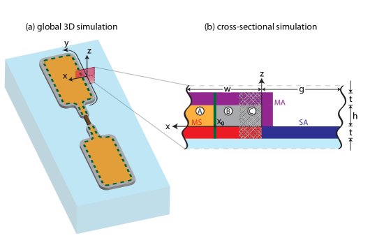
To avoid this divergence, we first divide the electrode pads and the associated MS and MA surfaces into “perimeter regions” and “interior regions” [Fig. S1(a,b)] with their boundary set at a constant distance (, typically 1 m) from the edge. (The SA surface can be similarly divided by a contour at a constant distance from the outside of the edge. The treatment of the SA surface is otherwise analogous to that of MS.) In a global coarse 3D simulation, electric field in the interior regions does not have sharp variations, and therefore easily converges to spatial distributions that we may immediately record as and at the top and bottom surfaces of the electrode pads respectively. We use these field distributions to calculate the surface participation associated with the interior region of the pads (denoted by the subscript “int”):
| (S1) |
where = MS or MA, and is the total electric field energy in the entire space (dominated by energy in the substrate and vacuum). Here we have multiplied the field integral by the assumed thickness of the surface layer, = 3 nm, further assuming that the electric field is uniform across that thickness.
The perimeter regions can be described by a spatial coordinate as shown in Fig. S1(a,b), where the -axis winds around the edges of the pads, remaining tangent. We further divide the perimeter regions into two halves. Energy in the half adjacent to the edge fails to converge, regardless of initial mesh parameters, following the adaptive mesh refinement process. The other half can be made to converge using mesh parameters that are computationally accessible. The key concept to our strategy is to employ a constant ratio, or “scaling factor” , to convert the integrated field energy in the convergent half into that of the entire perimeter regions, so that
| (S2) |
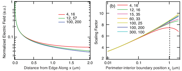
The spatial distribution of electric field in the perimeter region can be written using separation of variables as in the limit of . This is because the electric field near a metal edge should have a local scaling property independent of distant electromagnetic boundary conditions. Here describes the edge scaling that can be applied to any cross section, independent of y. The actual form of depends on material thicknesses and dielectric constants and is difficult to derive analytically. However, we can compute in a 2D cross-sectional electrostatic simulation of an electrode pad, which focuses on the metal edge and takes account of the actual thicknesses of each material [Fig. S1(b)]. The reduced dimensionality allows for accurate computation of the field inside the surface layer using sub-nm spatial resolution. In this simulation we choose boundary conditions representative of the width of the pad () and the spatial separation between the opposing electrodes (). Although such a cross-sectional simulation does not accurately reflect the boundary condition in 3D space, as we already noted, is independent of the distant boundary conditions as long as . As an illustration, is shown in Fig. S2(a) for a few very different values of and .
For our devices with electrode pads typically 10 to 500 m in their smallest dimension, and separations on about the same scale, the above edge scaling function is a very good approximation within the perimeter region for properly chosen . From we can calculate the scaling factor based on the ratios of integrated field energy within the cross section:
| (S3) |
| (S4) |
Scaling factors for various extents of the perimeter region are shown in Fig. S2(b). We limit our method in the regime of , where is insensitive to the values of and . In practice, we use m for most of the pad structure (which are at least 10 m in width and separation). Inserting these simulated scaling factors into Eq. (S2) allows one to arrive at .
I.2 Surfaces associated with the junction leads
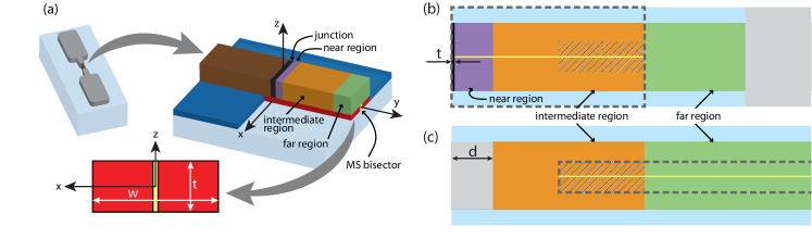
A schematic of the Josephson junction and the leads is shown in Fig. S3(a), where -axis and -axis are defined perpendicular and parallel to the leads, respectively. We divide the surfaces associated with the junction leads into three regions based on distance from the junction: the near region ( m), the intermediate region (1 m m), and the far region ( m). The surface participation ratios for these regions are denoted by , and respectively (as shown in Table S1), where = MS, MA or SA. The near region of the leads is not explicitly included in the global simulation. The intermediate and far regions are included in the global simulation, but the surface integration of field energy does not converge due to the influence of edges. A scaling factor solution akin to that in Section A demands , but the lead is too narrow and too close to the junction to satisfy this. We use a supplemental local 3D simulation of the junction leads as shown in Fig. S3(a), which includes the thicknesses of all materials, to compute the surface participation of all three regions surrounding the leads.
This high-resolution local simulation is performed by applying an electrostatic voltage potential between the pair of leads across the junction. The boundary of the local simulation is set sufficiently far (typically 25 m) to ensure the calculated field distribution in the the near and intermediate regions is not affected by the type of boundary condition used. The overall magnitude of electric field in this local simulation is arbitrarily set by the imposed voltage, and must be rescaled by a constant to be consistent with the field scale of the global simulation from which is obtained.
This constant can be determined by comparing with the field distribution in the global simulation in a selected overlapping region (“stitching extent”) where both simulations are reliable. In particular, we choose the stitching extent as the center line of the leads in the 5 m region [Fig. S3(b)]. Such a choice avoids the numerical imprecision of the global simulation in areas close to the junction or the edges. It also avoids any artificial boundary effects of the local simulation by remaining distant from the boundary. We confirmed the two simulations show consistent spatial dependence over this stitching extent, , and the constant is computed from the ratio of the two.
Surface participation ratios for the near and intermediate regions of the leads can then be immediately calculated by integrating over the volume of interest. For example,
| (S5) |
The surface participation ratios from the near and intermediate regions are expected to be independent of the design of the electrodes, and therefore show very little change among all the devices reported in this study (Table S1).
On the other hand, Eq. S5 does not apply to lead energies in the far region, which is not fully included in the local simulation. To calculate we adopt a separation-of-variables approach by noting that = . Here describes the cross-sectional distribution of electric field in dimensionless units (normalized by the field magnitude at the center line of the lead) [Fig. S3(a)]. It can be obtained from the local simulation of the junction leads discussed above, which also confirms that is independent of for m. Therefore,
| (S6) |
where the second integral effectively produces a constant factor that converts the electric field at a single point of the center line into energy per unit length along . This factor is equal to m2 for the typical lead width of 1 m.
II Fabrication methods
Fabrication of qubits were performed using the Dolan bridge technique Dolan (1977) on 430 um thick c-plane EFG sapphire wafers. After cleaning in acetone and methanol, the wafer was spun with a bilayer of e-beam resist consisting of 550 nm of MMA EL13 and 70 nm of PMMA A3, then baked at 175 ∘C. A 13 nm aluminum film was then evaporated as an anti-charging layer for electron beam lithography. Patterning of the qubit was done on a 100 kV VISTEC EBPG 5000+ e-beam writer. The anti-charging layer was removed with TMAH, and the wafer was subsequently developed for 55 seconds in 1:3 MIBK:IPA followed by a 10 second rinse in IPA. The wafer was then loaded into a Plassys e-beam evaporation system (MEB550S or UMS 300). After a 40 W Ar/O2 3:1 plasma cleaning for 30 seconds, without breaking vacuum, a bi-layer of aluminum (20 nm and 60 nm) was deposited using double-angle evaporation. In between the two layers, the junction barrier was grown by thermal oxidation using a Ar/O2 85%/15% mixture at 15 Torr for 12 minutes. Finally, the aluminum was capped with another oxide layer grown with the same mixture at 3 Torr for 10 minutes. After deposition, liftoff was performed in 60 ∘C NMP for several hours, then rinsed with acetone and methanol. Prior to dicing, a layer of photoresist was spun on the wafer to protect the qubits. After dicing in an ADT ProVecturs 7100 dicer, the resist was removed by rinsing in acetone and methanol.
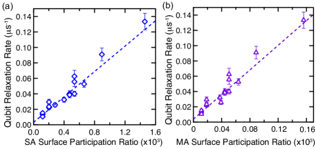
III Qubit lifetime vs. SA & MA participation ratios
In the main text, we presented the linear relationship between qubit relaxation rates () and the MS surface participation ratio (). Since for all our qubit designs, MA, MS and SA surface participation ratios change approximately in proportion [Fig. 3(b) of the main text], qubit also shows similar linear relationship with or , as shown in Fig. S4. Assuming SA or MA is the only lossy surface, linear fits to the two data sets indicate or respectively. Since any of the three surfaces can be responsible for the qubit relaxation, these values, together with obtained from Fig. 3(a) of the main text, should be considered upper bounds for these dielectric surfaces. Furthermore, since a combination of the three has to explain the strongly-correlated changes in , we conclude . Linear fits in Fig. S4(a,b) also give residual (geometry-independent) relaxation rates of ms-1 and ms-1 respectively, consistent with the value obtained from Fig. 3(a).
IV Estimate of surface participation in planar qubits
In the main text, we placed a number of reported transmon qubits from literature on a diagram of versus (Fig. 4) for comparison with devices in this study. For most planar transmons included in the figure, we do not have complete knowledge of the geometric parameters related to all aspects of their design (e.g. junction leads, coupling to the ground plane, device package, etc.) to perform a full-scale simulation. However, since surface participation ratios for most planar transmons are dominated by capacitor pads with approximate translational symmetry (i.e. having a longitudinal dimension much larger than the lateral dimension), we can estimate their from cross-sectional simulations alone, similar to the previous work on CPW resonators Sandberg et al. (2012); Wenner et al. (2011). Horizontal error bars of represents uncertainties that can be caused by variations in parameters not captured in such a simulation. The planar capacitors that we have simulated fall into three styles: interdigitated capacitor (IDC) Chang et al. (2013); Houck et al. (2008); Geerlings (2013); Riste et al. (2015), coplanar waveguide (CPW) Barends et al. (2013); Kelly et al. (2015) and coplanar capacitor (CPC) Chow et al. (2014). All three styles can be simulated in settings similar to Fig. S1(b) with different choices of boundary conditions.
In the context of translation-symmetric planar structures, the surface participation ratios are predominantly controlled by the width () of the capacitor electrodes and the gap () between them. Assuming and are varied in proportion, the surface participation ratios are approximately inversely proportional to or . (More rigorously, , where is related to the thicknesses of the metal film () and the surface dielectric layers (). For MS interface and for nm, nm, nm.) Therefore, it is convenient to express (inverse) surface participation ratios in the form of an effective length scale, . We define , or “effective IDC pitch width”, of a qubit under study as the width (w) of an IDC structure (with g=w) with identical metal-substrate participation ratio. This effective width has been used as the top axis in Fig. 4 of the main text, whose relationship to is calibrated through cross-sectional simulations of IDC structures. We also find the surface participation of CPW and CPC structures with are equivalent to IDC structures with in both cases. An advantage of using is that surface participation ratios across different devices can be compared without assuming hypothetical thicknesses and dielectric constants of the surface dielectric layers.
The uncertainties of for these qubits reported from other institutions are based on the stated uncertainties, provided sample statistics, or the variations as a function of frequency (for frequency-tunable qubits).
References
- Nigg et al. (2012) S. E. Nigg, H. Paik, B. Vlastakis, G. Kirchmair, S. Shankar, L. Frunzio, M. H. Devoret, R. J. Schoelkopf, and S. M. Girvin, Physical Review Letters 108, 240502 (2012).
- Barends et al. (2013) R. Barends, J. Kelly, A. Megrant, D. Sank, E. Jeffrey, Y. Chen, Y. Yin, B. Chiaro, J. Mutus, C. Neill, P. OâMalley, P. Roushan, J. Wenner, T. C. White, A. N. Cleland, and J. M. Martinis, Physical Review Letters 111, 080502 (2013).
- Chang et al. (2013) J. B. Chang, M. R. Vissers, A. D. Córcoles, M. Sandberg, J. Gao, D. W. Abraham, J. M. Chow, J. M. Gambetta, M. B. Rothwell, G. A. Keefe, M. Steffen, and D. P. Pappas, Applied Physics Letters 103, 012602 (2013).
- Dolan (1977) G. J. Dolan, Applied Physics Letters 31, 337 (1977).
- Sandberg et al. (2012) M. Sandberg, M. R. Vissers, J. S. Kline, M. Weides, J. Gao, D. S. Wisbey, and D. P. Pappas, Applied Physics Letters 100, 262605 (2012).
- Wenner et al. (2011) J. Wenner, R. Barends, R. C. Bialczak, Y. Chen, J. Kelly, E. Lucero, M. Mariantoni, A. Megrant, P. J. J. OâMalley, D. Sank, A. Vainsencher, H. Wang, T. C. White, Y. Yin, J. Zhao, A. N. Cleland, and J. M. Martinis, Applied Physics Letters 99, 113513 (2011).
- Houck et al. (2008) A. A. Houck, J. A. Schreier, B. R. Johnson, J. M. Chow, J. Koch, J. M. Gambetta, D. I. Schuster, L. Frunzio, M. H. Devoret, S. M. Girvin, and R. J. Schoelkopf, Physical Review Letters 101, 080502 (2008).
- Geerlings (2013) K. Geerlings, Ph.D. thesis (Yale University, 2013).
- Riste et al. (2015) D. Riste, S. Poletto, M.-Z. Huang, A. Bruno, V. Vesterinen, O.-P. Saira, and L. DiCarlo, Nature Communications 6, 6983 (2015).
- Kelly et al. (2015) J. Kelly, R. Barends, A. G. Fowler, A. Megrant, E. Jeffrey, T. C. White, D. Sank, J. Y. Mutus, B. Campbell, Y. Chen, Z. Chen, B. Chiaro, A. Dunsworth, I.-C. Hoi, C. Neill, P. J. J. OâMalley, C. Quintana, P. Roushan, A. Vainsencher, J. Wenner, A. N. Cleland, and J. M. Martinis, Nature 519, 66 (2015).
- Chow et al. (2014) J. M. Chow, J. M. Gambetta, E. Magesan, D. W. Abraham, A. W. Cross, B. R. Johnson, N. A. Masluk, C. A. Ryan, J. A. Smolin, S. J. Srinivasan, and M. Steffen, Nature Communications 5, 4015 (2014).