Comparison of GaN nanowires grown on c-, r- and m-plane sapphire substrates
Abstract
Gallium nitride nanowires were grown on c-plane, r-plane and m-plane sapphire substrates in a showerhead metalorganic chemical vapor deposition system using nickel catalyst with trimethylgallium and ammonia as precursors. We studied the influence of carrier gas, growth temperature, reactor pressure, reactant flow rates and substrate orientation in order to obtain thin nanowires. The nanowires grew along the 101 and 100 axes depending on the substrate orientation. These nanowires were further characterized using x-ray diffraction, electron microscopy, photoluminescence and Raman spectroscopy.
keywords:
GaN, nanowire, growth, MOCVD, nickel catalyst, sapphire substrates1 Introduction
Gallium nitride (GaN) nanowires (NWs) have been of interest for nanoscale photonic [1, 2, 3, 4, 5, 6, 7]and electronic [8, 9, 10]device applications. The growth of GaN NWs by catalyst mediated [8, 9, 11, 12, 13] as well as catalyst free [6, 14, 15, 16] methods have been reported. Unlike InAs, where 111 oriented wires are usually obtained [17, 18, 19], III-nitride NW growth has been observed along different crystal directions and is strongly dependent on growth conditions, the substrate and its orientation.
In most of the reports of GaN NW growth the axis along the nanowire length (or the growth direction) is along either the polar 0001 direction (i.e. c-axis) or the non-polar directions 110 (a-axis) and 100 (m-axis). On (0001) c-plane sapphire, Gottschalch [11] reported the growth of vertical wires growing along c-axis using gold as catalyst, while Ji [20] obtained wires growing along the a-axis with nickel catalyst. On (102) r-plane sapphire using nickel-catalysed metalorganic chemical vapor deposition (MOCVD), Zhou obtained wires tilted on the substrate and growing along m-axis.[12] On the other hand, Wang [13] and Qian [4] reported the growth NWs along the a-axis on r-plane sapphire with nickel catalyst. The growth of inclined GaN nanorods along the c-axis using m-plane (100) sapphire as substrate without any foreign catalyst was reported recently.[16, 21] There are very few reports on the growth of GaN NWs along semipolar directions. The growth along the semi-polar 101 direction has been reported on c-plane sapphire by Park by reaction of metallic Ga and gaseous NH3 by using nickel as the catalyst.[22] Peng also reported growth along 101 but on graphite substrates, using a mixture of Ga2O3 and C along with NH3 as precursor, by a hot-filament CVD, without any catalyst.[23] Tessarek obtained GaN wires via a self-catalyzed method by MOCVD, on different planes of sapphire, namely c-, r- a- and m-plane. These wires grew invariably along the c-axis with diameters more than 200 nm.[21] There are, however, hardly any reports that compare GaN NW growth on different substrate orientations in the same run. We report the growth of thin, nickel-catalysed, GaN NWs on c-, r- and m-plane sapphire substrates under identical conditions. We studied the dependence of growth direction on the substrate orientation with other growth conditions kept similar, and characterized the samples using electron microscopy, x-ray diffraction, photoluminescence and Raman spectroscopy.
2 Growth of nanowires
GaN NWs were grown using MOCVD with nickel catalyst and trimethylgallium (TMGa) and ammonia (NH3) as precursors. The substrates were cleaned, drop-coated with nickel nitrate hexahydrate solution ( 0.01 M), blow-dried with N2 gas and annealed in hydrogen to form metallic nickel nanoparticles which subsequently served as the catalyst particle.[13, 24] This method to form the catalyst particles is more convenient than techniques involving evaporation of nickel or gold. The size of the catalyst particle can be controlled by the annealing time and temperature (See Supplementary Information section II for details). Since the exact composition and phase (solid/liquid) of the nickel-gallium alloy that serves as the catalyst during growth is unknown, the NW growth mechanism could be either vapour-liquid-solid (VLS) or vapour-solid-solid (VSS). From a post-growth compositional analysis of the catalyst particle (not presented here), we believe that at the growth temperatures used in our experiments (C) GaN NW growth happens via a VSS process. We also tried to grow GaN NWs using gold nanoparticles as catalyst. Gold catalysed wires grew slower than their nickel assisted counterparts under similar growth conditions, as reported by Zhou .[12]
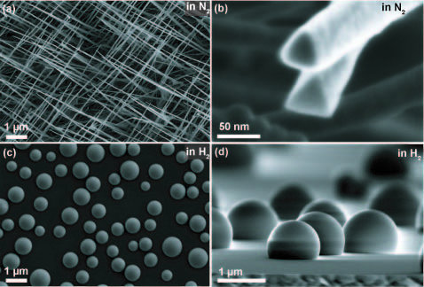
We varied the temperature, reactor pressure and rate of flow of precursors in order to obtain thin and non-tapering NWs. The growth of NWs was sensitive to the reactor conditions. We first discuss the effect of carrier gas on growth. After annealing the nickel nitrate hexahydrate coated sapphire substrates in a hydrogen environment to produce nickel nanoparticles, we could grow GaN NWs in a pure nitrogen ambient. The scanning electron micrograph (SEM) of the NWs is shown in Figure 1(a). The wires typically had a triangular cross section (Figure 1(b)). However, under similar reactor conditions in an H2 ambient or in a mixture of equal volumes of N2 and H2, we did not obtain any wires. Instead, we obtained just hemispherical gallium droplets (Figure 1(c),(d)), unlike earlier reports.[10]
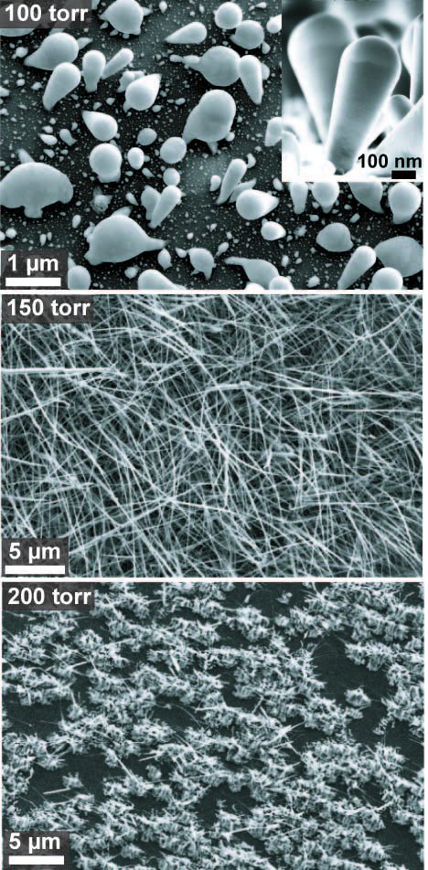
NWs were grown on different orientations of sapphire namely c-plane, r-plane and m-plane. The NWs obtained from the same growth run at C and 150 torr with 45 mol/min (1 sccm) NH3 flow and 7.8 mol/min (2 sccm) TMGa flow on these substrates are shown in Figure 2. On these substrates we obtained NWs as thin as 20 nm diameter with a triangular cross section. The growth temperature was varied between C and C. Experiments carried out at different reactor pressures between 50 torr and 200 torr (Figure 3) showed that long thin NWs were obtained at 150 torr. At a relatively low pressure of 100 torr icecream-cone shaped structures were formed. A lot of wires grown at 175 torr had kinks or had a zig-zag morphology. At 200 torr there were very little NW growth, and those few were highly tapered and short. Very low flow of precursors (7.8-9.7 mol/min of TMGa and 45 mol/min of NH3) and small V/III ratio () was used to facilitate anisotropic growth. At large V/III ratio the growth is slower, while at low V/III ratio the NWs obtained are more tapered. (For SEM images refer Supporting Information Section I.) We found that a pressure of 150 torr in N2 environment, C and a V/III ratio of was optimum for obtaining thin non-tapering wires.

A comparison of the NWs obtained on different planes which are shown in Figure 2 is given in Table 1. All these samples compared are from the same growth run (at C and 150 torr with 45 mol/min NH3 flow and 7.8 mol/min TMGa flow). The length of the NWs were determined by imaging cross sectional samples. The NWs obtained on c-plane sapphire are narrower than the NWs on r-plane. On m-plane sapphire we see two distinct set of NWs – one which is narrow (thickness 30 nm) and one which is thicker (thickness 90 nm). Since the NWs on m-plane sapphire are not erect, it is difficult to measure its exact length, but they are longer than NWs grown on c- and r-plane.
| Sapphire | Nanowire | Average (mode) | Average (mode) | Low temp. |
|---|---|---|---|---|
| substrate | growth | of length | of diameter | PL FWHM |
| orientation | direction | (m) | (nm) | (meV) |
| r-plane | 100 | 2.5 | 40 | 390 |
| c-plane | 100 | 3 | 25 | 220 |
| m-plane | 101, 100 | 13 | 30, 90 | 350 |
3 Structural characterization of nanowires
The crystal structure and the crystallinity of the NWs were analyzed using x-ray diffraction (XRD) and transmission electron microscopy (TEM).
3.1 XRD analysis
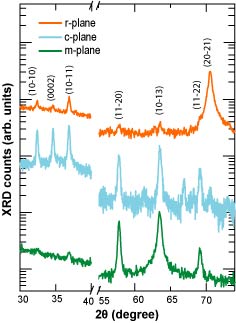
The grazing incidence XRD pattern the GaN nanowires grown on c-plane, r-plane and m-plane sapphire substrates is shown in Figure 4. The peaks are quite sharp indicating good crystal quality. The peak positions have been indexed to the wurtzite crystal structure of GaN. The lattice constants obtained by least square fitting from the peak positions were a = 3.188 Å and c = 5.179 Åwhich agrees with values reported in literature.[25, 26]
3.2 TEM analysis

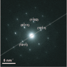
The crystallinity and growth direction of the wires grown on c-, m- and r-plane sapphire were determined using TEM. Since the NW thickness is less than 100 nm they are electron transparent and do not require further thinning down for TEM studies. The sample on which wires were grown was ultrasonicated in methanol to make a suspension. This suspension was slowly dropped multiple times onto a TEM grid and the solvent allowed to evaporate. The presence of the catalyst nanoparticle seen at the end of the wire in the TEM image (Figure 5 (a)) confirms that the growth was catalytic. From energy dispersive X-ray spectroscopy the presence of Ga in the catalyst along with Ni was confirmed. The lattice planes seen in the high resolution TEM images (Figure 5(b)) and the well-defined electron diffraction pattern obtained (Figure 5(c)) confirm the single crystal nature of these wires. The diffraction pattern was indexed to find the lattice planes that gave rise to the diffraction spots. By comparing the diffraction pattern and the low magnification TEM image of the wire, the growth axis was determined. An indexed electron diffraction pattern obtained with a TEM is shown in Figure 6 showing that the growth direction is 101 for this wire. The wires grew along the m-axis (100) on both c-plane (Figure 5(c)) and r-plane sapphire substrates. On m-plane sapphire most of the NWs grew along the 101 (Figure 6) and 100 directions (Table 1).
4 Optical characterization
The optical properties of the GaN NWs were studied using photoluminescence (PL) spectroscopy from ensembles of NWs. The sample was excited with a 266 nm frequency-quadrupled Nd:YAG laser. The luminescence from the sample was dispersed through a 0.55 m monochromator and detected with a thermoelectrically cooled Si-CCD.
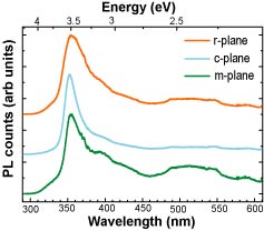
The PL spectra of GaN NWs at 10 K grown on c-plane, r-plane and m-plane sapphire are shown in Figure 7. The spectra are normalized such that the near-band-edge emission peak is of the same intensity. PL spectra from these NWs peak around 3.50 eV (354 nm), which corresponds to the near-band-edge emission of GaN.[20, 27, 28] The FWHM of the PL peaks are 22 nm (220 meV), 42 nm (390 meV) and 37 nm (350 meV) for NWs grown on c-plane, r-plane and m-plane sapphire respectively. These FWHM values are comparable to those reported in literature.[29, 30] The width of these spectra could be due to the variation in thickness and properties of the different wires of the ensemble,[20] or due to defect-related luminescence.[31] An additional peak is observed at 3.1 eV (400 nm) which might be due to strongly localized excitons.[31]. Yellow luminescence from these samples is relatively small indicating good crystal quality.
5 Raman spectroscopy of NWs
Raman spectroscopy was used to study the phonon modes of GaN NWs. A Witec alpha 300R confocal Raman microscope was used with a 532 nm frequency doubled Nd:YAG laser for excitation.
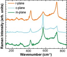
Figure 8 shows the Raman spectra for single GaN NWs, that were transferred to an aluminium foil which serves as the substrate. Al foil was chosen as substrate since it provides much lesser background signal in the region of interest than conventional crystalline substrates like Si, GaAs, sapphire, etc and other amorphous substrates. The intensity of the Raman peaks depends on the direction of both the incident and scattered polarization vectors relative to the crystal orientation. In order to observe as many phonons as possible from NWs from all samples the incident electric field was set at an angle of with the NW axis, and the scattered light of all polarizations were detected simultaneously. (The spectra shown is after background correction.) Difference in relative intensity may due to difference in growth direction of NW and/or because the incident light might be falling in different direction relative to the crystallographic directions.
At around 144, 567 and 734 cm-1 the E2 (low), E2 (High) and E1 (LO) are seen.[32, 33, 34] These peaks are allowed by group theory in a infinitely large sample with wurtzite crystal structure belonging to the space group (P63mc), and has been observed experimentally in first order Raman spectra. But, the other peaks observed in the spectrum shown (Figure 8) arise due to the finite dimensions of the NWs. The acoustic phonons, and also the combination of both acoustic and low-lying optical branches at the M symmetry point in the Brillouin zone gives rise to the spectral peak around 256 cm-1.[35] The peak at 308 cm-1 arises from the overtone process of acoustic phonons and the energy position matches the flat phonon branch at the H-point in the Brillouin zone. The peak observed in the spectra at 418 cm-1 also is an acoustic overtone corresponding to the M-point.[36, 37, 35, 33] The Raman peaks are broader compared to those reported in bulk samples due to the finite size effects in accordance with the phonon confinement model, where the spatial confinement of phonons in nanocrystals leads to an uncertainty in wave vector and hence a broadening of the Raman spectral lines.[38, 39, 35]
6 Conclusions
In conclusion, we have grown GaN NWs on c-plane, m-plane, and r-plane sapphire substrates using nickel catalyst and TMGa and NH3 as precursors by MOCVD. A pressure of 150 torr in N2 environment and C, with low precursor flow rates and V-III ratio, was optimum for growing thin, non-tapering GaN NWs. The wires had a triangular cross-section and grew along the 101 and 100 directions. Low temperature PL shows near-band-edge emission from the NWs and small yellow luminescence indicates good crystalline quality. Raman spectra reveals the good crystal quality of these NWs and effects due to finite size.
7 Acknowledgments
The authors are thankful to Mandar Deshmukh, Priti Gupta, Sandip Ghosh, Ritam Sinha and S.C. Purandare at TIFR, India and Subramaniyam Nagarajan at Aalto University, Finland for support in materials characterization and useful discussions. This work at TIFR was supported through internal grants 12P0168 and 12P0169. C.B.M. acknowledges travel support from the Department of Science and Technology, India, through the collaborative project INT/Finland/P-10.
References
References
- [1] Justin C. Johnson, Heon-Jin Choi, Kelly P. Knutsen, Richard D. Schaller, Peidong Yang, and Richard J. Saykally. Single gallium nitride nanowire lasers. Nature Materials, 1(2):106–110, October 2002.
- [2] Xiangfeng Duan, Yu Huang, Ritesh Agarwal, and Charles M. Lieber. Single-nanowire electrically driven lasers. Nature, 421(6920):241–245, January 2003.
- [3] Fang Qian, Yat Li, Silvija , Deli Wang, Carl J. Barrelet, and Charles M. Lieber. Gallium nitride-based nanowire radial heterostructures for nanophotonics. Nano Letters, 4(10):1975–1979, October 2004.
- [4] Fang Qian, Yat Li, Silvija , Hong-Gyu Park, Yajie Dong, Yong Ding, Zhong Lin Wang, and Charles M. Lieber. Multi-quantum-well nanowire heterostructures for wavelength-controlled lasers. Nature Materials, 7(9):701–706, September 2008.
- [5] M. Tchernycheva, A. Messanvi, A. de Luna Bugallo, G. Jacopin, P. Lavenus, L. Rigutti, H. Zhang, Y. Halioua, F. H. Julien, J. Eymery, and C. Durand. Integrated photonic platform based on InGaN/GaN nanowire emitters and detectors. Nano Letters, 14(6):3515–3520, June 2014.
- [6] Wei Guo, Meng Zhang, Animesh Banerjee, and Pallab Bhattacharya. Catalyst-free InGaN/GaN nanowire light emitting diodes grown on (001) silicon by molecular beam epitaxy. Nano Letters, 10(9):3355–3359, September 2010.
- [7] Ju-Ying Chen, Tong-Ming Wong, Che-Wei Chang, Chen-Yuan Dong, and Yang-Fang Chen. Self-polarized spin-nanolasers. Nature Nanotechnology, 9(10):845–850, October 2014.
- [8] Yu Huang, Xiangfeng Duan, Yi Cui, and Charles M. Lieber. Gallium nitride nanowire nanodevices. Nano Letters, 2(2):101–104, February 2002.
- [9] Zhaohui Zhong, Fang Qian, Deli Wang, and Charles M. Lieber. Synthesis of p-type gallium nitride nanowires for electronic and photonic nanodevices. Nano Letters, 3(3):343–346, March 2003.
- [10] Yat Li, Jie Xiang, Fang Qian, Silvija , Yue Wu, Hao Yan, Douglas A. Blom, and Charles M. Lieber. Dopant-free GaN/AlN/AlGaN radial nanowire heterostructures as high electron mobility transistors. Nano Letters, 6(7):1468–1473, July 2006.
- [11] V. Gottschalch, G. Wagner, J. Bauer, H. Paetzelt, and M. Shirnow. VLS growth of GaN nanowires on various substrates. Journal of Crystal Growth, 310(23):5123–5128, November 2008.
- [12] Xiang Zhou, Jordan Chesin, Samuel Crawford, and Silvija . Using seed particle composition to control structural and optical properties of GaN nanowires. Nanotechnology, 23(28):285603, July 2012.
- [13] George T. Wang, A. Alec Talin, Donald J. Werder, J. Randall Creighton, Elaine Lai, Richard J. Anderson, and Ilke Arslan. Highly aligned, template-free growth and characterization of vertical GaN nanowires on sapphire by metal–organic chemical vapour deposition. Nanotechnology, 17(23):5773, December 2006.
- [14] R. Koester, J. S. Hwang, C. Durand, D. Le Si Dang, and J. Eymery. Self-assembled growth of catalyst-free GaN wires by metal–organic vapour phase epitaxy. Nanotechnology, 21(1):015602, January 2010.
- [15] T. Aschenbrenner, C. Kruse, G. Kunert, S. Figge, K. Sebald, J. Kalden, T. Voss, J. Gutowski, and D. Hommel. Highly ordered catalyst-free and mask-free GaN nanorods on r-plane sapphire. Nanotechnology, 20(7):075604, February 2009.
- [16] Sooryong Chae, Kyuseung Lee, Jongjin Jang, Daehong Min, Jaehwan Kim, and Okhyun Nam. Self-assembled growth of inclined GaN nanorods on (10−10) m-plane sapphire using metal–organic chemical vapor deposition. Journal of Crystal Growth, 409:65–70, January 2015.
- [17] K. Hiruma, M. Yazawa, T. Katsuyama, K. Ogawa, K. Haraguchi, M. Koguchi, and H. Kakibayashi. Growth and optical properties of nanometer‐scale GaAs and InAs whiskers. Journal of Applied Physics, 77(2):447–462, January 1995.
- [18] Linus E. Jensen, Mikael T. , Sören Jeppesen, Ann I. Persson, B. Jonas Ohlsson, and Lars Samuelson. Role of surface diffusion in chemical beam epitaxy of InAs nanowires. Nano Letters, 4(10):1961–1964, October 2004.
- [19] Bernhard Mandl, Julian Stangl, Thomas Mårtensson, Anders Mikkelsen, Jessica Eriksson, Lisa S. Karlsson, Günther Bauer, Lars Samuelson, and Werner Seifert. Au-free epitaxial growth of InAs nanowires. Nano Letters, 6(8):1817–1821, August 2006.
- [20] Hangfeng Ji, Martin Kuball, Robert A. Burke, and Joan M. Redwing. Vibrational and optical properties of gan nanowires synthesized by ni-assisted catalytic growth. Nanotechnology, 18(44):445704, November 2007.
- [21] C. Tessarek, S. Figge, A. Gust, M. Heilmann, C. Dieker, E. Spiecker, and S. Christiansen. Optical properties of vertical, tilted and in-plane GaN nanowires on different crystallographic orientations of sapphire. Journal of Physics D: Applied Physics, 47(39):394008, October 2014.
- [22] Eunmi Park, Sojung Shim, Ryong Ha, Eunsoon Oh, Byoung Woo Lee, and Heon-Jin Choi. Reassembling of Ni and Pt catalyst in the vapor–liquid–solid growth of GaN nanowires. Materials Letters, 65(15–16):2458–2461, August 2011.
- [23] H. Y Peng, X. T Zhou, N Wang, Y. F Zheng, L. S Liao, W. S Shi, C. S Lee, and S. T Lee. Bulk-quantity GaN nanowires synthesized from hot filament chemical vapor deposition. Chemical Physics Letters, 327(5–6):263–270, September 2000.
- [24] Wolfgang Brockner, Claus Ehrhardt, and Mimoza Gjikaj. Thermal decomposition of nickel nitrate hexahydrate, ni(NO3)2·6h2o, in comparison to co(NO3)2·6h2o and ca(NO3)2·4h2o. Thermochimica Acta, 456(1):64–68, May 2007.
- [25] M. Leszcynski, I. Grzegory, and M. Bockowski. X-ray examination of GaN single crystals grown at high hydrostatic pressure. Journal of Crystal Growth, 126(4):601–604, February 1993.
- [26] I. Vurgaftman and J. R. Meyer. Band parameters for nitrogen-containing semiconductors. Journal of Applied Physics, 94(6):3675–3696, September 2003.
- [27] B. Monemar. Fundamental energy gap of GaN from photoluminescence excitation spectra. Physical Review B, 10(2):676–681, July 1974.
- [28] Lawrence H. Robins, Kris A. Bertness, Joy M. Barker, Norman A. Sanford, and John B. Schlager. Optical and structural study of GaN nanowires grown by catalyst-free molecular beam epitaxy. i. near-band-edge luminescence and strain effects. Journal of Applied Physics, 101(11):113505, June 2007.
- [29] S. C. Lyu, O. H. Cha, E. K. Suh, H. Ruh, H. J. Lee, and C. J. Lee. Catalytic synthesis and photoluminescence of gallium nitride nanowires. Chemical Physics Letters, 367(1–2):136–140, January 2003.
- [30] Alan H. Chin, Tai S. Ahn, Hongwei Li, Sreeram Vaddiraju, Christopher J. Bardeen, Cun-Zheng Ning, and Mahendra K. Sunkara. Photoluminescence of GaN nanowires of different crystallographic orientations. Nano Letters, 7(3):626–631, March 2007.
- [31] Michael A. Reshchikov and Hadis Morkoç. Luminescence properties of defects in GaN. Journal of Applied Physics, 97(6):061301, March 2005.
- [32] T. Azuhata, T. Sota, K. Suzuki, and S. Nakamura. Polarized Raman spectra in GaN. Journal of Physics: Condensed Matter, 7(10):L129, March 1995.
- [33] V. Yu. Davydov, Yu. E. Kitaev, I. N. Goncharuk, A. N. Smirnov, J. Graul, O. Semchinova, D. Uffmann, M. B. Smirnov, A. P. Mirgorodsky, and R. A. Evarestov. Phonon dispersion and raman scattering in hexagonal GaN and AlN. Physical Review B, 58(19):12899–12907, November 1998.
- [34] Claudia Bungaro, Krzysztof Rapcewicz, and J. Bernholc. Ab initio phonon dispersions of wurtzite AlN, GaN, and InN. Physical Review B, 61(10):6720–6725, March 2000.
- [35] Chia-Chun Chen, Chun-Chia Yeh, Chun-Ho Chen, Min-Yuan Yu, Hsiang-Lin Liu, Jih-Jen Wu, Kuei-Hsein Chen, Li-Chyong Chen, Jin-Yuan Peng, and Yang-Fang Chen. Catalytic Growth and Characterization of Gallium Nitride Nanowires. Journal of the American Chemical Society, 123(12):2791–2798, March 2001.
- [36] Byeongchul Ha, Sung Ho Seo, Jung Hee Cho, Chong S. Yoon, Jinkyoung Yoo, Gyu-Chul Yi, Chong Yun Park, and Cheol Jin Lee. Optical and field emission properties of thin single-crystalline GaN nanowires. The Journal of Physical Chemistry B, 109(22):11095–11099, June 2005.
- [37] H. Siegle, G. Kaczmarczyk, L. Filippidis, A. P. Litvinchuk, A. Hoffmann, and C. Thomsen. Zone-boundary phonons in hexagonal and cubic GaN. Physical Review B, 55(11):7000–7004, March 1997.
- [38] H. Richter, Z. P. Wang, and L. Ley. The one phonon Raman spectrum in microcrystalline silicon. Solid State Communications, 39(5):625–629, August 1981.
- [39] T. Kanata, H. Murai, and K. Kubota. Raman and xâ€ray scattering from ultrafine semiconductor particles. Journal of Applied Physics, 61(3):969–971, February 1987.