Current address: ]Nepal Academy of Science and Technology, Khumaltar, Lalitpur, Nepal.
A systematic study of structural, electronic and optical properties of atomic scale defects in 2D transition metal dichalcogenides MX2 (M = Mo,W; X = S, Se, Te)
Abstract
In this work, we have systematically studied structural, electronic and magnetic properties of atomic scale defects in 2D transition metal dichalcogenides \ceMX2, (M = Mo and W; X = S, Se and Te) by density functional theory. Various types of defects, e.g., X vacancy, X interstitial, M vacancy, M interstitial, MX and XX double vacancies have been considered. It has been found that the X interstitial has the lowest formation energy ( 1 eV) for all the systems in the X–rich condition whereas for M–rich condition, X vacancy has the lowest formation energy except for \ceMTe2 systems. Both these defects have very high equilibrium defect concentrations at growth temperatures (1000K-1200K) reported in literature. A pair of defects, e.g., two X vacancies or one M and one X vacancies tend to occupy the nearest possible distance. No trace of magnetism has been found for any one of the defects considered. Apart from X interstitial, all other defects have defect states appearing in the band gap, which can greatly affect the electronic and optical properties of the pristine systems. Our calculated optical properties show that the defect states cause optical transitions at 1.0 eV, which can be beneficial for light emitting devices. The results of our systematic study are expected to guide the experimental nanoengineering of defects to achieve suitable properties related to band gap modifications and characterization of defect fingerprints via optical absorption measurements.
I Introduction
Ever since the first successful fabrication of graphene, a single layered honeycomb structure of carbon atoms by Novoselov et al. in 2004Novoselov et al. (2004), there has been a continuous increase in research interests on many other 2D monolayers.Apart from grapheneO’Hare et al. (2012) other extensively studied single layered systems are silicene Okamoto et al. (2010); Sugiyama et al. (2010); Yang and Ni (2005); O’Hare et al. (2012); Rachel and Ezawa (2014), germanene O’Hare et al. (2012); Li et al. (2014); Cai et al. (2013); Rachel and Ezawa (2014), staneneXu et al. (2013); van den Broek et al. (2014); Rachel and Ezawa (2014), phosphorene Liu et al. (2014); Das et al. (2014) and a number of single layered transition metal dichalcogenides (MX2, M = Transition metal and X = Chalcogen) Ugeda et al. (2014a); Mak et al. (2010); Zeng et al. (2012). These single layered systems, having two dimensional (2D) structures, generally exhibit properties, which are remarkably different from their respective three dimensional bulk phases and thus these systems have become important subjects for experimental and theoretical studies. From the application point of view, the 2D semiconducting systems have the minimum possible thickness and wide band gaps, which make them important for photovoltaics, sensing, biomedicine, solar cells and catalysis.
It is not uncommon to find atomic scale defects in 2D materials, e.g., in graphene, mono and di-vacancies, Stone-Wales defects etc. have been studied quite extensively. Vacancies are formed during the fabrication of monolayer MoS2 using sonochemical deposition method. It is known that these vacancies have considerable effects on electronic, magnetic and optical properties. For example MoS2 has been found to acquire S vacancies during its fabrication. These S vacancies are found to be detrimental for n-type conductivity of MoS2 as they create deep trap states for electronsZhou et al. (2013); Noh et al. (2014). Moreover, the concentration of defects depends on the mode of the fabrication process. For example, the carrier mobility in MoS2 monolayer fabricated by chemical vapor deposition method is 0.02 cm2/V-sLee et al. (2012) whereas in mechanically exfoliated monolayer, it can go up to 10 cm2/V-sRadisavljevic et al. (2011). Owing to the importance of role of defects, there are few recent theoretical studies of native defects in MoS2Noh et al. (2014); Zhou et al. (2013); Dang and Spearot (2014). Tongay et al. have investigated the effect of anion vacancy on photoluminescence of MoS2, MoSe2 and WSe2 using experiment and density functional theory calculations. Tongay et al. (2013) Recently Liu and coworkers have studied the influence of anion and metal vacancies on electronic and optical properties of monolayer MoS2.ping Feng et al. (2014) Various defects in monolayer \ceMoS2 have been investigated previously by means of first principles DFT calculations by different groups Zhou et al. (2013); Ghorbani-Asl et al. (2013); Komsa et al. (2013); Komsa and Krasheninnikov (2015); KC et al. (2014); Ataca and Ciraci (2011). Rotational defects have also been studied theoretically and experimentally recently on \ceMoSe2 and \ceWSe2 by Lin et al. Lin et al. (2015)
However, to the best of our knowledge, systematic studies on the role of various point defects and double defects on the electronic and optical properties of transition metal dichalcogenides are not available in the literature.
Therefore, in this paper we have systematically investigated the role of defects in modifying the electronic and optical properties of monolayers of transition metal dichalcogenides, MX2 (M = Mo, W and X = S, Se, Te). We present the most probable defects under various growth conditions, the electronic structures of defected materials and the signature of these defects in optical properties. The paper is organized in the following way. First, we present the computational details followed by the results of optimized structures in presence of defects. Then we report formation energies and equilibrium defect concentrations. Finally, we present electronic structures of defected monolayers and their optical signatures.
II Computational Details
II.1 Basic parameters
All the calculations have been performed with a monolayer MX2 supercell, where M stands for Mo, W and X stands for S, Se, Te. We have considered both M and X defects (in terms of vacancy or interstitial) in all of the above systems. The supercell is generated by repeating the primitive cell by five times in and directions. A vacuum of 20 Å is included to avoid the interaction between periodic images in the out-of-plane direction. The calculations have been performed using a plane-wave based density functional code vasp. Kresse and Furthmüller (1996) The generalized gradient approximation of Perdew, Burke and Ernzerhof Perdew et al. (1996, 1997) has been used for the exchange-correlation potential. The structures have been optimized using the conjugate gradient method with the forces calculated using the Hellman-Feynman theorem. The energy and the Hellman-Feynman force thresholds have been kept at 10-5 eV and 10-2 eV/Å respectively. For geometry optimizations, a 3 3 1 Monkhorst-Pack -grid is used. Total energies and electronic structures are calculated with the optimized structures on a 5 5 1 Monkhorst-Pack -grid. It is worth mentioning that some defect states may result in finite magnetic moments. For that purpose, we have considered spin-polarization in all our calculations. However, all the systems relaxed to non magnetic ground states. Spin-orbit coupling was not included.
| MoS2 | MoSe2 | MoTe2 | WS2 | WSe2 | WTe2 | ||
|---|---|---|---|---|---|---|---|
| (Å) | PBE | 3.18 | 3.32 | 3.56 | 3.18 | 3.32 | 3.56 |
| Expt. | 3.16 | 3.30 | 3.52 | 3.15 | 3.28 | – | |
| PBE | 1.73 | 1.47 | 1.08 | 1.89 | 1.58 | 1.09 | |
| Expt. | 1.95 | 1.58 | 1.1 | 1.99 | 1.65 | – |
Using the above parameters we have computed the in-plane lattice constants and band gaps of different pristine \ceMX2 systems. These computed values along with the experimental values have been tabulated in table 1. Our calculated lattice constants and band gaps are in good agreement with the previous theoretical calculations Wang et al. (2012); KC et al. (2014); Komsa and Krasheninnikov (2015); Ramasubramaniam (2012); Kang et al. (2013)
II.2 Defect formation energy
The defect formation energy is defined as follows.
| (1) |
where is the total energy of the MX2 supercell with defects and is the total energy of the MX2 supercell without any defect. denotes the number of element (M or X atoms) added to or removed (with a negative sign) from the pristine system to create defects. is the chemical potential of the element .
To compute the chemical potential, we have used the formula , where and are the chemical potentials for M and X respectively. The total energy per formula unit of the pristine monolayer MX2 is denoted as . For M rich environment, , where is the total energy of a bcc M metal per atom. Thus, can be computed as . For the X rich environment, , where is the energy per atom of the bulk crystal of X. Therefore, is computed as .
II.3 Optical properties
The optical properties are also calculated using the vasp code. Kresse and Furthmüller (1996). The optical properties of these materials can be described using the complex dielectric constant: . The dielectric function has been computed in the momentum representation by obtaining the matrix elements between occupied and unoccupied eigenstates. The imaginary part of the dielectric function can be derived from the following formula: Gajdoš et al. (2006)
| (2) |
where the indices and denote, respectively, the conduction and valence band states. The cell periodic part of the wavefunctions at the given -point is denoted by . The real part of the dielectric function is obtained by using Kramers-Kronig transformation:
| (3) |
where P and denote, respectively, the principal value and the complex shift.
III Results and Discussions
III.1 Geometry & Energetics
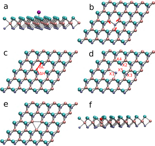
We have compared six different types of defects for various MX2 (M = Mo,W; X = S,Se,Te) systems. The defects are as follows – X-vacancy, X-interstitial, M-vacancy, M-interstitial, XX-vacancy and MX-vacancy in each monolayer MX2 system. To find out the ground state structures, we have considered many possible starting geometries to find out the lowest energy structure for each of the system. In the following sections, we will first discuss the optimized geometries and energetics of point defects followed by the double defects. In Fig. 1 we have shown the typical lowest energy optimized structures of all the different defects that we have considered for the present study.
Point defects
X – interstitial
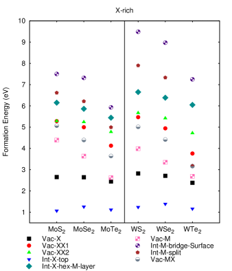
Fig. 1(a) represents the energetically most stable X interstitial defect (Xi) structure. Our calculation of formation energy (See Fig. 2) reveals that under both X–rich and M–rich conditions, the most stable structure is found to have Xi adatom attached to the top of a host X atom (Xh). We have considered two other interstitial positions for Xi adatom – (i) hexagonal position at the M layer and (ii) bridge position between two host X atoms at the top layer. For Xi adatom on top of Xh atom structures, the formation energies are 1.1 eV for all MX2 defects for X–rich environment. However, for M–rich environment, the formation energy drops from 2.4 eV (X = S) to 1.3 eV (for X = Te). The formation energies for the hexagonal position are 6 eV for all MX2 systems, which are quite high compared to the Xi adatom attached to the top of Xh atom. Our calculation also shows that the above mentioned bridge position is a metastable position and after relaxation, the Xi adatom moves to the top of Xh adatom. The Xi–Xh bond lengths are 1.94 Å, 2.26 Å and 2.65 Å, respectively for X = S, X = Se and X = Te.
X – vacancy
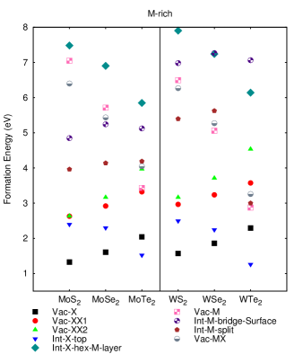
The most stable structure of X vacancy is shown in Fig. 1(b). The vacancy is created by removing one X atom in the single layer MX2 supercell. The absence of one X atom causes the three M atoms to relax towards the vacancy site. M–X bond lengths change by 0.04 Å and 0.02 Å respectively for MoX2 and WX2 systems. Under X–rich environment, the formation energy of X vacancy in MoTe2 is 0.21 eV smaller than for MoSe2 and MoS2. The same for WTe2 is 0.44 eV and 0.33 eV smaller than the WSe2 and WS2 respectively. However, formation energy of X vacancy in MTe2 is higher than MSe2 and MS2 under M–rich environment.
M – vacancy
| Length (Å) | MoS2 | MoSe2 | MoTe2 | WS2 | WSe2 | WTe2 |
|---|---|---|---|---|---|---|
| 0.10 | 0.00 | -0.12 | 0.11 | 0.05 | -0.09 | |
| -0.02 | -0.09 | -0.56 | -0.02 | -0.08 | -0.53 | |
| -0.05 | -0.02 | 0.01 | -0.05 | -0.03 | 0.01 |
Fig. 1(c) represents the energetically most stable structure of M vacancy. As the M atom was connected to six X atoms, there are six dangling bonds of X atom present in the structure affecting the relaxation of these X atoms. Table 2 refers to the length variation due to creation of the M vacancy. The analysis of length variation shows that while the S and Se atoms relaxed outwards from the vacancy center, the Te atoms relaxed inwards to the vacancy center. Also, the vertical height between the Te atoms from the top and bottom layer reduces by a large amount ( 0.5 Å) compared to the S and Se atoms. The reason behind these geometry changes is that the S and Se are more electronegative compared to Te. Hence the dangling S/Se atoms repel each other strongly leading to the outward relaxation from the vacancy center. For Te atoms, although they repel each other, there is a bigger void to fill in due to the M vacancy. Hence for \ceMTe2 system, we observe an inward relaxation. These geometry changes directly influence the vacancy formation energies, where MTe2 has the lowest formation energy compared to MS2 and MSe2 under both X–rich and M–rich environment.
M – interstitial
| MoS2 | MoSe2 | MoTe2 | WS2 | WSe2 |
|---|---|---|---|---|
| 2.11 | 2.06 | 1.97 | 2.24 | 2.23 |
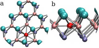
Finally, we show the ground state geometry for M interstitial in Fig. 1(f). We have considered two different interstitial positions of M atom. In one case, we have inserted the M atom at the bridge position in between two X atoms and in the other case, the M atom was inserted in the split interstitial position along the direction. Our calculated formation energy shows that the split interstitial position is energetically most favorable except WTe2. Table 3 shows the bond length variations for M–Mi for the split interstitial position of different \ceMX2 systems. Fig. 3 shows the top and side views of energetically favorable structure of W interstitial defect in WTe2, which is quite different from the structure described above. In this case, the interstitial atom resides at the hexagonal position in the M layer forming a distorted hexagon.
Double defects
MX – vacancy
| Length (Å) | MoS2 | MoSe2 | MoTe2 | WS2 | WSe2 | WTe2 |
|---|---|---|---|---|---|---|
| 0.22 | 0.08 | -0.35 | 0.23 | 0.16 | 0.08 | |
| -0.05 | -0.26 | -0.49 | -0.02 | -0.15 | 0.08 | |
| -0.12 | -0.12 | -0.13 | -0.12 | -0.12 | -0.13 |
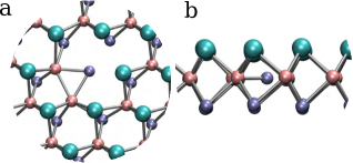
For a MX di-vacancy (created by removing adjacent M and X atoms), the most stable structure is shown in Fig. 1(d). Due to the removal of M and X atoms, five neighboring X atoms around the vacancy site relax during the optimization process. Table 4 shows the amount of relaxation of these X atoms with dangling bonds. After geometry optimization, X1 atom in general moves towards the M layer reducing the M–X1 bond length for all the systems. For MX2 (X = S, Se), the X2 and X3 atoms relax outward from the vacancy site while X4 and X5 atoms relax inward mainly because of the missing X atom in that layer. The reason for these relaxation behavior is similar to the case of M vacancy. For \ceMoTe2, the dangling X atom relaxes inward. However, for \ceWTe2 system they relax slightly outward because of the fact that X1 atom moves to M layer and forms an isosceles triangle with two M atoms with bond length 2.6 Å. Fig. 4 shows the slanted top and side views of this particular geometry. The formation energy of MX vacancy is lower for MTe2 for both X and M rich environment.
XX – vacancy
The most stable structure of XX di-vacancy is shown in Fig. 1(e). We have considered two different configurations for XX vacancy. In one configuration, we have removed two X atoms (with same x and y coordinates) from the top and bottom layers (vac–XX1) and in the other configuration, two nearest X atoms have been removed from the same layer (vac–XX2). The calculation of formation energies indicates that the vac–XX1 structure is energetically more favorable compared to vac–XX2 structure. Here we find that the M atoms relax inward to the vacancy site and form an equilateral triangle with bond length 2.8 Å.
| XX11 | XX12 | XX13 | XX21 | XX22 | MX1 | MX2 | |
|---|---|---|---|---|---|---|---|
| \ceMoS2 | 0.0 | 0.13 | 0.04 | 0.00 | 0.05 | 0.0 | 2.02 |
| \ceMoSe2 | 0.0 | 0.45 | 0.32 | 0.24 | 0.35 | 0.0 | 1.88 |
| \ceMoTe2 | 0.0 | 0.99 | 0.83 | 0.64 | 0.86 | 0.0 | 1.59 |
| \ceWS2 | 0.0 | 0.31 | 0.18 | 0.2 | 0.21 | 0.0 | 1.89 |
| \ceWSe2 | 0.0 | 0.68 | 0.50 | 0.47 | 0.54 | 0.0 | 1.95 |
| \ceWTe2 | 0.0 | 1.32 | 1.03 | 0.96 | 1.08 | 0.0 | 1.84 |
| XX11 | XX12 | XX13 | XX21 | XX22 | MX1 | MX2 | |
|---|---|---|---|---|---|---|---|
| \ceMS2 | 3.12 | 4.46 | 6.33 | 3.18 | 5.59 | 2.41 | 3.99 |
| \ceMSe2 | 3.34 | 4.71 | 6.65 | 3.32 | 5.75 | 2.54 | 4.18 |
| \ceMTe2 | 3.60 | 5.07 | 7.14 | 3.56 | 6.17 | 2.73 | 4.49 |
To investigate the dependence of distance on the formation energies of XX- and MX-vacancies, we have calculated defect formation energies for various distances between a pair of defects. In table 5, relative energies as a function of distances are tabulated. XX1 and XX2 vacancies denote two X atoms removed from different layers and same layers of X atom, respectively, from a pristine \ceMX2 system. XX11, XX12 and XX13 are three different XX1 configurations considered with three different distances between X atoms where XX11 corresponds to the nearest neighbor configuration. In a same manner, XX21 and XX22 are two different XX2 configurations considered. For MX vacancy also we have considered two different distances – MX1 and MX2 where MX1 is the nearest neighbor. Our results clearly show that the double vacancies always prefer to form when they are within the nearest neighbor distance signifying the natural occurrence of correlated vacancies. A clear trend of increasing formation energies while one goes down in the periodic table from S to Te is observed for both Mo and W in case of anion vacancies. The trend is not absolutely clear for M-X vacancies.
III.2 Equilibrium defect concentration
We have also calculated equilibrium defect concentrations for all the defects. The equilibrium defect concentration, , can be calculated using the occupation probability as shown below,
| (4) |
where is the concentration of possible defect sites, is the formation energy of the defect and is the temperature (1000K – 1200K) during the crystal growth.
| Xint | Xvac | Mint | Mvac | MXvac | XXvac | |
|---|---|---|---|---|---|---|
| \ceMoS2 | 9.2–7.2 | 96.7–1.6 | 5.1–1.8 | 8.4–4.1 | 6.3–1.1 | 2.7–7.3 |
| \ceMoSe2 | 1.0–1.1 | 1.1–1.8 | 5.4–8.9 | 5.3–0.6 | 1.6–7.9 | 7.5–1.2 |
| \ceMoTe2 | 5.1–4.5 | 1.1–1.2 | 7.6– 1.2 | 67.1–1.1 | 9.9–1.14 | 1.8–5.2 |
| \ceWS2 | 1.2–1.4 | 13.7–3.2 | 1.7–7.5 | 8.9–1.2 | 1.2–2.0 | 3.1–1.2 |
| \ceWSe2 | 2.2–3.3 | 48.6–9.2 | 1.3–1.8 | 1.5–9.78 | 1.2–6.4 | 1.4–1.9 |
| \ceWTe2 | 3.0–2.9 | 2.2–2.2 | 0.1–47.6 | 32.2–5.8 | 0.3–1.1 | 1.3–0.2 |
| Xint | Xvac | Mint | Mvac | MXvac | XXvac | |
|---|---|---|---|---|---|---|
| \ceMoS2 | 1.8–1.9 | 4.8–6.2 | 1.2–2.6 | 3.4–2.9 | 1.3–3.0 | 64.6 – 1.0 |
| \ceMoSe2 | 5.8–5.0 | 1.8–4.1 | 1.6–4.7 | 1.8–1.1 | 9.2–3.4 | 2.2–6.3 |
| \ceMoTe2 | 4.8–9.1 | 1.2–6.0 | 8.8–2.9 | 5.8–4.4 | 9.2–2.3 | 2.0– 12.6 |
| \ceWS2 | 6.0–7.5 | 2.8–5.8 | 7.3–2.5 | 2.1–6.0 | 5.9–1.1 | 1.3 –4.0 |
| \ceWSe2 | 1.1–8.4 | 9.8–3.6 | 5.2–2.7 | 3.7–6.5 | 6.1–1.6 | 5.6–29.3 |
| \ceWTe2 | 1.0–1.2 | 6.4–5.4 | 0.9–2.9 | 3.7–9.6 | 8.5–46.7 | 1.1–1.1 |
In Tables 6 and 7, we have tabulated the range of equilibrium defect concentrations for a range of growth temperatures (1000K – 1200K) for X–rich and M–rich conditions respectively. This range of temperature is chosen as most of the \ceMX2 monolayer structures are synthesized experimentally in this range. Ling et al. (2014); Wang et al. (2014a, b); Pradhan et al. (2014); Zhang et al. (2013); Huang et al. (2014). Our calculation clearly shows that the presence of defect under the X–rich condition and defect under the M–rich condition during the crystal growth is very much likely. However the probability of forming defect under X–rich condition and the formation of defect under M–rich condition is very low.
III.3 Electronic properties

In this section, we will discuss the electronic properties of the defected MX2 structures by analyzing total density of states (DOS), site and projected densities of states (PDOS) and partial charge densities.
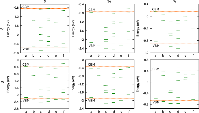
In Fig. 5, we have shown an energy level diagram for all the different defect states in all \ceMX2 systems constructed from our calculated data. In each subplot, the columns (a)-(f) represent the (a) X–interstitial, (b) X–vacancy, (c) M–vacancy, (d) MX–vacancy, (e) XX–vacancy and (f) M–interstitial defect respectively. The orange long dashed line denote the position of valence band maxima (VBM) and conduction band minima (CBM) of the pristine \ceMX2 systems. The short green solid and dashed lines denote the position of defect states for both occupied and unoccupied states respectively. From the analysis of energy level diagram, it can be seen that the defect states mainly appear in the gap region of the pristine system. Further analysis of DOS for all the defects in all the \ceMX2 systems reveals that for a specific defect, the qualitative behavior is very much similar between \ceMoS2/\ceWS2, \ceMoSe2/\ceWSe2 and \ceMoTe2/\ceWTe2. Furthermore, our analysis shows that the qualitative electronic properties due the presence of defects in \ceMoS2/\ceMoSe2 are quite similar. Hence we have shown the DOS, PDOS analysis for only \ceMoS2 and \ceMoTe2 systems.
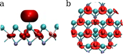
The analysis of density of states for X interstitial defects for all the systems shows the same qualitative behavior. In Fig. 6(c), we have shown the total densities of states for two systems – MoS2 and MoTe2. The general observation is that the defect states are found near the band edges. These states merge with both valence and conduction bands. To find the orbital character of these defect states, we have carried out the analysis of site projected density of states (PDOS) and partial charge density analysis. Figs. 6(a) and 6(b) show the partial charge density for valence band maximum (VBM) and conduction band minimum (CBM) respectively. Our analysis shows that the states near the VBM mainly arise from Xi atom. These states are the doubly degenerately occupied and orbitals. There are also very small contributions of in-plane M – and states appearing in the VBM. The states near the CBM originate mainly from the M – orbitals with some contribution from the unoccupied orbital of Xi atom.
Fig. 7 shows density of states for X vacancy defects for MoS2 and MoTe2. For X vacancy defects, the features of density of states in the valence band side are identical for all the MX2 systems. In these systems, the defect state appears at the valence band edge and inside the band gap towards the conduction band side. The defect states can be further classified as singlet state (near valence band) and doubly degenerate state (the empty localized state in the gap) due to the trigonal symmetry of the X vacancy. The analysis of on-site projected DOS reveals that these states are formed from the combination of diagonal out of plane orbitals ( and ) and in-plane orbitals ( and ) of the M atoms near the defected sites and very small amount of in-plane orbitals (mainly ) of second nearest neighbor X atoms. The orbital characters of VBM and CBM are respectively contributed by the and orbitals of the M atom.
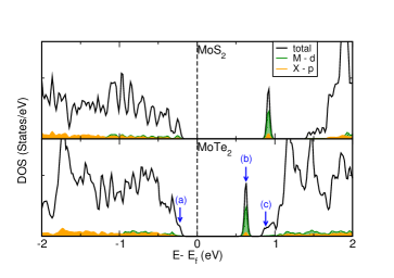
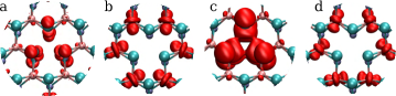
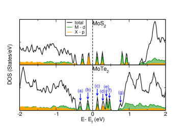
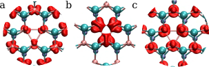
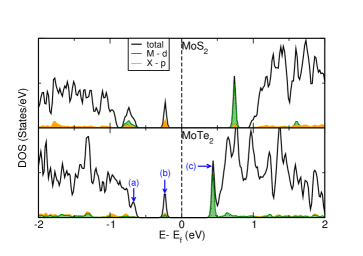
The analysis of PDOS and partial charge density shows that the defect states due to the M vacancy appear inside the gap region. The density of states for M vacancy in MoS2 and MoTe2 systems are shown in Fig. 8. In this case, singlet and doublet defect states can be seen due to the trigonal and mirror symmetry of M vacancy and two layers of X atoms, respectively. The VBM contains both the orbital (significant contribution) of the six X atoms near the vacancy site and orbitals of the M atoms (see Fig. 8(a)). The defect peak (marked as (b) in DOS) is a doublet state and originates mainly from the and orbitals of the six M atoms (second near neighbor from the vacancy site). The other defect peak (marked as (c) in the DOS) originates from the orbital of the six X atoms near the vacancy site along with very small orbital contribution from the M atoms. The CBM mainly contains the and orbitals of the M atoms. All these states are formed due to the local perturbation created in the geometry due to the absence of one M atom.
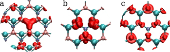
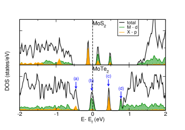
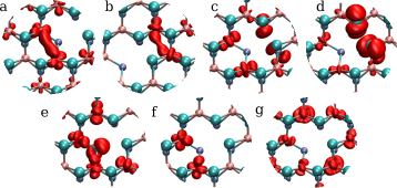
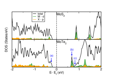
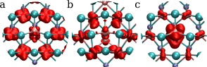
In Fig. 9, we have shown the MX–vacancy density of states comparison for \ceMoS2 and \ceMoTe2 as well as the partial charge density for the defect states, VBM and CBM. For MX vacancy, combined defect states due to M–vacancy and X–vacancy can be observed. As seen for the figure (see Fig. 9), the defect states appear mainly in the gap region. This defect has a strong influence on conduction band of \ceMX2. The states marked as (a) and (b) in the DOS) are mainly originating from the and orbital of the M atoms near the vacancy site. A mix orbital character of , form the M atom and in-plane orbital from the dangling X atom can be observed in defect peak (c). However, the major contribution to the defect peak (d) is coming from the orbitals of the dangling X atom with a minor contribution from orbital of M atom. The defect peak (e) is again a mixture of , of M atom and of the X atom. However, the defect peak (f) is mainly of character with and are being the dominant orbitals. The CBM mainly consists of orbital of M atoms.
For the XX double vacancy also the defect states can be seen in the gap region. Fig. 10 shows the comparison of densities of states for MoS2 and MoTe2 and the partial charge densities of \ceMoTe2 system for this defect. The analysis of partial charge density and PDOS shows that these defect states are the combined effect of two single X vacancies. Consequently, the characteristic features of the defect peaks are very much similar to the X–vacancy defects as discussed previously.
The density of states for Mo interstitial in \ceMoS2 and \ceMoTe2 and the partial charge density for the \ceMoTe2 have been shown in Fig. 11. The general trend in the density of states for Mo interstitial defect in \ceMX2 system is again very similar for all the systems. The defect levels are generated inside the band gap. The occupied states are one doublet and one singlet state and the unoccupied state is the doublet state. The contribution to the occupied defect states are mainly coming from the orbital of the interstitial M atom and the M atom attached with it. There is also a smaller contribution from the neighboring M atom’s orbital. However, the contribution to the unoccupied defect state is manly from the defect site M atom’s and orbitals.
III.4 Optical properties

In addition to the geometric and electronic structures, we have also studied the influence of defects in the optical properties of defected \ceMX2 by means of frequency dependent dielectric functions. In the following paragraphs we will briefly discuss the comparison of optical properties for the pristine system followed by the modification of optical properties due to the presence of defects.
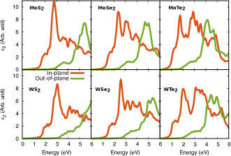
The comparison of optical properties for all the pristine \ceMX2 systems have been shown in Fig. 12. We have plotted the imaginary parts of the dielectric functions with their in-plane ( and ) and out of plane () components as a function of energy. The and components have the same absorption spectra for all the systems and their absorption is stronger than the component. From the figure, it can be seen that the general features of the optical spectra for same X elements are quite similar in nature with a step like peak followed by a dominant peak, valley and subsequent peaks. This step like peak is the characteristic of a two-dimensional system. From the analysis of the spectra, it can be seen that the prominent optical peak shifts towards lower energy and breaks into more than one peak as we move towards the heavier X element (see fig. 12). The step like peak also moves towards lower energy with heavier X element, signifying smaller band gaps.
Introduction of defects in the pristine \ceMX2 system can affect the optical properties also. From our calculations, we have found out that most notable change in the optical properties due to the presence of defect occurs for three following defects – i) M–vacancy, ii) X–vacancy and iii) MX–vacancy. Therefore, in the following section we have discussed aforementioned defects only.
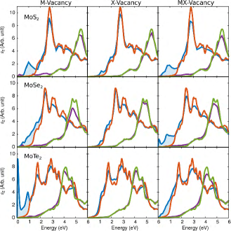
In Fig. 13 and Fig. 14, we have shown the comparison of optical properties for M–, X– and MX–vacancies for \ceMoX2 and \ceWX2 respectively. As mentioned before, here also the and components have the same absorption spectra for all the systems and their absorption is stronger than the component.
For M–vacancy in \ceMoS2, the defect peaks appear just below and above the Fermi level (see fig. 8), which have mainly and characters and are responsible for the electronic transition. This transition occurs at 1.0 eV. In \ceMoSe2, the peak is broader as there are two possible transitions possible with a very small energy interval. However for M–vacancy in \ceMoTe2, the defect peak appears at the Fermi energy (see fig. 8) giving rise to a sharp optical transition at a very low energy (see fig. 13).
For X–vacancy, the defect state appears very close to the CBM of pristine system (see fig. 7). Thus the optical spectra with X–vacancy in different \ceMoX2 systems do not change significantly from the pristine one. In the case of MX–vacancy also a number of defect peaks appear near the Fermi energy for all \ceMoX2 systems (See fig. 9) which give rise to the electronic transition at 0.5 eV with a relatively broader peak distribution than M–vacancy.
The analysis of DOS for \ceWX2 systems (figure not shown) show similar characteristics as of \ceMoX2. This leads to a very much similar optical properties as shown in Fig. 14 as compared to \ceMoX2 (Fig. 13).
The calculated dielectric functions elicit that the absorption spectrum appears in the visible region (3 eV–1.7 eV (400–700 nm)) for \ceMX2 systems. It is well known that the material, which has absorption in the visible region is suitable for photocatalysis using sunlight. Therefore, \ceMX2 having suitable defects can be used for the photocatalysis. Tongay et al. Tongay et al. (2013) in their study have investigated effects of anion vacancy on the photoluminescence of \ceMoS2, \ceMoSe2 and \ceWS2 where this vacancy is identified by a new peak appearing below the photoluminescence peak. Moreover, the intensity of the photoluminescence peak enhances with increasing defect density. As we discussed above, the absorption spectra of both M–vacancy and MX–vacancy defected \ceMX2 have new peaks at 1.0 eV and 0.5 eV, respectively, which arise due to the defect states. This feature is very much similar to that observed with anion vacancy. Nowadays, it is possible to create point defects in 2D materials (as demonstrated in graphene) using ion-irradiation technique. One may speculate that the creation of suitable defects in \ceMX2 may give rise to desired optical transitions suitable for light emitting diodes.
IV Conclusions
We have performed a systematic study of native defects, viz. X vacancy, X interstitial, M vacancy, M interstitial, MX vacancy and XX vacancy on a single layer of \ceMX2 system (M = Mo, W; X = S, Se, Te) using first principles density functional theory. It has been found that under X–rich condition, X interstitial defect has the lowest formation energy for all the systems under investigation with equilibrium defect concentration cm-2 at the growth temperature range of 1000-1200K. For M–rich environment, X vacancy has the lowest formation energy except \ceMTe2 systems, where X interstitial defect has the lowest formation energy. Metal atom and double vacancy related defects are quite high in formation energy thus showing almost zero equilibrium defect concentration at the studied growth temperatures. Our calculations reveal the position of defect states in the band gap along with the orbitals contributing to those states. Finally, our calculated optical properties indicate prominent signatures in the in-plane component of the imaginary part of the dielectric functions. One may speculate that suitably designed defected \ceMX2 systems can be promising materials for light emitting devices.
Acknowledgement
OE acknowledges KAW foundation for financial support. In addition, BS acknowledges Carl Tryggers Stiftelse, Swedish Research Council and KOF initiative of Uppsala University for financial support. SH also acknowledges valuable discussions with Carmine Autieri. We are grateful to NSC under Swedish National Infrastructure for Computing (SNIC) and the PRACE project resource Cy-Tera supercomputer based in Cyprus at the Computation-based Science and Technology Research Center (CaSToRC) and Zeus supercomputer based in Poland at the academic computer center Cyfronet. Structural figures were generated using VMD Humphrey et al. (1996).
References
- Novoselov et al. (2004) K. S. Novoselov, A. K. Geim, S. V. Morozov, D. Jiang, Y. Zhang, S. V. Dubonos, I. V. Grigorieva, and A. A. Firsov, Science 306, 666 (2004), http://www.sciencemag.org/content/306/5696/666.full.pdf .
- O’Hare et al. (2012) A. O’Hare, F. V. Kusmartsev, and K. I. Kugel, Nano Letters 12, 1045 (2012), pMID: 22236130, http://dx.doi.org/10.1021/nl204283q .
- Okamoto et al. (2010) H. Okamoto, Y. Kumai, Y. Sugiyama, T. Mitsuoka, K. Nakanishi, T. Ohta, H. Nozaki, S. Yamaguchi, S. Shirai, and H. Nakano, Journal of the American Chemical Society 132, 2710 (2010), pMID: 20121277, http://dx.doi.org/10.1021/ja908827z .
- Sugiyama et al. (2010) Y. Sugiyama, H. Okamoto, T. Mitsuoka, T. Morikawa, K. Nakanishi, T. Ohta, and H. Nakano, Journal of the American Chemical Society 132, 5946 (2010), http://dx.doi.org/10.1021/ja100919d .
- Yang and Ni (2005) X. Yang and J. Ni, Phys. Rev. B 72, 195426 (2005).
- Rachel and Ezawa (2014) S. Rachel and M. Ezawa, Phys. Rev. B 89, 195303 (2014).
- Li et al. (2014) L. Li, S.-z. Lu, J. Pan, Z. Qin, Y.-q. Wang, Y. Wang, G.-y. Cao, S. Du, and H.-J. Gao, Advanced Materials 26, 4820 (2014).
- Cai et al. (2013) Y. Cai, C.-P. Chuu, C. M. Wei, and M. Y. Chou, Phys. Rev. B 88, 245408 (2013).
- Xu et al. (2013) Y. Xu, B. Yan, H.-J. Zhang, J. Wang, G. Xu, P. Tang, W. Duan, and S.-C. Zhang, Phys. Rev. Lett. 111, 136804 (2013).
- van den Broek et al. (2014) B. van den Broek, M. Houssa, E. Scalise, G. Pourtois, V. V. Afanas‘ev, and A. Stesmans, 2D Materials 1, 021004 (2014).
- Liu et al. (2014) H. Liu, A. T. Neal, Z. Zhu, Z. Luo, X. Xu, D. Tománek, and P. D. Ye, ACS Nano 8, 4033 (2014), pMID: 24655084.
- Das et al. (2014) S. Das, W. Zhang, M. Demarteau, A. Hoffmann, M. Dubey, and A. Roelofs, Nano Letters 14, 5733 (2014).
- Ugeda et al. (2014a) M. M. Ugeda, A. J. Bradley, S.-F. Shi, F. H. da Jornada, Y. Zhang, D. Y. Qiu, W. Ruan, S.-K. Mo, Z. Hussain, Z.-X. Shen, F. Wang, S. G. Louie, and M. F. Crommie, Nature Materials 13, 1091 (2014a).
- Mak et al. (2010) K. F. Mak, C. Lee, J. Hone, J. Shan, and T. F. Heinz, Phys. Rev. Lett. 105, 136805 (2010).
- Zeng et al. (2012) H. Zeng, J. Dai, W. Yao, D. Xiao, and X. Cui, Nature Nanotechnology 7, 490 (2012).
- Zhou et al. (2013) W. Zhou, X. Zou, S. Najmaei, Z. Liu, Y. Shi, J. Kong, J. Lou, P. M. Ajayan, B. I. Yakobson, and J.-C. Idrobo, Nano Letters 13, 2615 (2013), pMID: 23659662, http://dx.doi.org/10.1021/nl4007479 .
- Noh et al. (2014) J.-Y. Noh, H. Kim, and Y.-S. Kim, Phys. Rev. B 89, 205417 (2014).
- Lee et al. (2012) Y.-H. Lee, X.-Q. Zhang, W. Zhang, M.-T. Chang, C.-T. Lin, K.-D. Chang, Y.-C. Yu, J. T.-W. Wang, C.-S. Chang, L.-J. Li, and T.-W. Lin, Advanced Materials 24, 2320 (2012).
- Radisavljevic et al. (2011) B. Radisavljevic, A. Radenovic, J. Brivio, V. Giacometti, and A. Kis, Nature Nanotechnology 6, 147 (2011).
- Dang and Spearot (2014) K. Q. Dang and D. E. Spearot, Journal of Applied Physics 116, 013508 (2014).
- Tongay et al. (2013) S. Tongay, J. Suh, C. Ataca, W. Fan, A. Luce, J. S. Kang, J. Liu, C. Ko, R. Raghunathanan, J. Zhou, F. Ogletree, J. Li, J. C. Grossman, and J. Wu, Sci. Rep. 3, 2657 (2013).
- ping Feng et al. (2014) L. ping Feng, J. Su, and Z. tang Liu, Journal of Alloys and Compounds 613, 122 (2014).
- Ghorbani-Asl et al. (2013) M. Ghorbani-Asl, A. N. Enyashin, A. Kuc, G. Seifert, and T. Heine, Physical Review B 88, 245440 (2013).
- Komsa et al. (2013) H.-P. Komsa, S. Kurasch, O. Lehtinen, U. Kaiser, and A. V. Krasheninnikov, Physical Review B 88, 035301 (2013).
- Komsa and Krasheninnikov (2015) H.-P. Komsa and A. V. Krasheninnikov, Physical Review B 91, 125304 (2015).
- KC et al. (2014) S. KC, R. C. Longo, R. Addou, R. M. Wallace, and K. Cho, , 1 (2014).
- Ataca and Ciraci (2011) C. Ataca and S. Ciraci, The Journal of Physical Chemistry C 115, 13303 (2011).
- Lin et al. (2015) Y.-C. Lin, T. Björkman, H.-P. Komsa, P.-Y. Teng, C.-H. Yeh, F.-S. Huang, K.-H. Lin, J. Jadczak, Y.-S. Huang, P.-W. Chiu, A. V. Krasheninnikov, and K. Suenaga, Nat Commun 6 (2015).
- Kresse and Furthmüller (1996) G. Kresse and J. Furthmüller, Phys. Rev. B 54, 11169 (1996).
- Perdew et al. (1996) J. P. Perdew, K. Burke, and M. Ernzerhof, Phys. Rev. Lett. 77, 3865 (1996).
- Perdew et al. (1997) J. P. Perdew, K. Burke, and M. Ernzerhof, Phys. Rev. Lett. 78, 1396 (1997).
- Böker et al. (2001) T. Böker, R. Severin, A. Müller, C. Janowitz, R. Manzke, D. Voß, P. Krüger, A. Mazur, and J. Pollmann, Phys. Rev. B 64, 235305 (2001).
- Schutte et al. (1987) W. Schutte, J. D. Boer, and F. Jellinek, Journal of Solid State Chemistry 70, 207 (1987).
- Mak et al. (2012) K. F. Mak, K. He, C. Lee, G. H. Lee, J. Hone, T. F. Heinz, and J. Shan, Nature Materials 12, 207 (2012).
- Soklaski et al. (2014) R. Soklaski, Y. Liang, and L. Yang, Applied Physics Letters 104, 193110 (2014).
- Zhang et al. (2014) Y. Zhang, T.-R. Chang, B. Zhou, Y.-T. Cui, H. Yan, Z. Liu, F. Schmitt, J. Lee, R. Moore, Y. Chen, H. Lin, H.-T. Jeng, S.-K. Mo, Z. Hussain, A. Bansil, and Z.-X. Shen, Nature nanotechnology 9, 111 (2014).
- Ugeda et al. (2014b) M. M. Ugeda, A. J. Bradley, S.-F. Shi, F. H. da Jornada, Y. Zhang, D. Y. Qiu, W. Ruan, S.-K. Mo, Z. Hussain, Z.-X. Shen, F. Wang, S. G. Louie, and M. F. Crommie, Nature Materials 13, 1091 (2014b), 1404.2331 .
- Ruppert et al. (2014) C. Ruppert, O. B. Aslan, and T. F. Heinz, Nano letters 14, 6231 (2014).
- Wang et al. (2015) Y. Wang, C. Cong, W. Yang, J. Shang, N. Peimyoo, Y. Chen, J. Kang, J. Wang, W. Huang, and T. Yu, Nano Research 8, 2562 (2015).
- Desai et al. (2014) S. B. Desai, G. Seol, J. S. Kang, H. Fang, C. Battaglia, R. Kapadia, J. W. Ager, J. Guo, and A. Javey, Nano Letters 14, 4592 (2014), http://dx.doi.org/10.1021/nl501638a .
- Wang et al. (2012) Q. H. Wang, K. Kalantar-Zadeh, A. Kis, J. N. Coleman, and M. S. Strano, Nature Publishing Group 7, 699 (2012).
- Ramasubramaniam (2012) A. Ramasubramaniam, Physical Review B 86, 115409 (2012).
- Kang et al. (2013) J. Kang, S. Tongay, J. Zhou, J. Li, and J. Wu, Applied Physics Letters 102, 012111 (2013).
- Gajdoš et al. (2006) M. Gajdoš, K. Hummer, G. Kresse, J. Furthmüller, and F. Bechstedt, Phys. Rev. B 73, 045112 (2006).
- Ling et al. (2014) X. Ling, Y.-H. Lee, Y. Lin, W. Fang, L. Yu, M. S. Dresselhaus, and J. Kong, Nano Letters 14, 464 (2014), pMID: 24475747, http://dx.doi.org/10.1021/nl4033704 .
- Wang et al. (2014a) S. Wang, Y. Rong, Y. Fan, M. Pacios, H. Bhaskaran, K. He, and J. H. Warner, Chemistry of Materials 26, 6371 (2014a), http://dx.doi.org/10.1021/cm5025662 .
- Wang et al. (2014b) X. Wang, Y. Gong, G. Shi, W. L. Chow, K. Keyshar, G. Ye, R. Vajtai, J. Lou, Z. Liu, E. Ringe, B. K. Tay, and P. M. Ajayan, ACS Nano 8, 5125 (2014b), pMID: 24680389, http://dx.doi.org/10.1021/nn501175k .
- Pradhan et al. (2014) N. R. Pradhan, D. Rhodes, S. Feng, Y. Xin, S. Memaran, B.-H. Moon, H. Terrones, M. Terrones, and L. Balicas, ACS Nano 8, 5911 (2014), pMID: 24878323, http://dx.doi.org/10.1021/nn501013c .
- Zhang et al. (2013) Y. Zhang, Y. Zhang, Q. Ji, J. Ju, H. Yuan, J. Shi, T. Gao, D. Ma, M. Liu, Y. Chen, X. Song, H. Y. Hwang, Y. Cui, and Z. Liu, ACS Nano 7, 8963 (2013), pMID: 24047054, http://dx.doi.org/10.1021/nn403454e .
- Huang et al. (2014) J.-K. Huang, J. Pu, C.-L. Hsu, M.-H. Chiu, Z.-Y. Juang, Y.-H. Chang, W.-H. Chang, Y. Iwasa, T. Takenobu, and L.-J. Li, ACS Nano 8, 923 (2014), pMID: 24328329, http://dx.doi.org/10.1021/nn405719x .
- Humphrey et al. (1996) W. Humphrey, A. Dalke, and K. Schulten, Journal of Molecular Graphics 14, 33 (1996).