Analog Computing Using Graphene-based Metalines
Abstract
We introduce the new concept of "metalines" for manipulating the amplitude and phase profile of an incident wave locally and independently. Thanks to the highly confined graphene plasmons, a transmit-array of graphene-based metalines is used to realize analog computing on an ultra-compact, integrable and planar platform. By employing the general concepts of spatial Fourier transformation, a well-designed structure of such meta-transmit-array combined with graded index lenses can perform two mathematical operations; i.e. differentiation and integration, with high efficiency. The presented configuration is about times shorter than the recent structure proposed by Silva et al. (Science, 2014, 343, 160-163); moreover, our simulated output responses are in more agreement with the desired analytic results. These findings may lead to remarkable achievements in light-based plasmonic signal processors at nanoscale instead of their bulky conventional dielectric lens-based counterparts.
keywords:
metalines, transmit-arrray, graphene plasmons, analog computing, Fourier transform, signal processorsRecently, realization of analog computing has been achieved by manipulating continuous values of phase and amplitude of the transmitted and reflected waves by means of artificial engineered materials, known as metamaterials, and planar easy-to-fabricate metamaterials with periodic arrays of scaterrers, known as metasurfaces 1, 2, 3. Both above-mentioned platforms offer the possibility of miniaturized wave-based computing systems that are several orders of magnitude thinner than conventional bulky lens-based optical processors 1, 4.
Challenges associated with the complex fabrication of metamaterials 5, 6, 7, 8, 9 besides absorption loss of the metal constituent of metasurfaces 10, 11, 12, 13, 14, degrade the quality of practical applications of relevant devices. As a result, graphene plasmonics can be a promising alternative due to the tunable conductivity of graphene and highly confined surface waves on graphene, the so-called graphene plasmons (GPs) 15, 16, 17, 18, 19, 20, 21.
We present a planar graphene-based configuration for manipulating GP waves to perform desired mathematical operations at nanoscale (see Figure 1). By applying appropriate external gate voltage and a well-designed ground plane thickness profile beneath the dielectric spacer holding the graphene layer, desired surface conductivity values are achieved at different segments of graphene layer 15, 22. To illustrate the applications of the proposed configuration, two analog operators, i.e. differentiator and integrator, are designed and realized. The proposed structure will be two dimensional which is an advantage compared to the previously reported three dimensional structures 1, 2, 3 that manipulate one dimensional variable functions.
We introduce a new class of meta-transmit-arrays (MTA) on graphene: metalines which are one dimensional counterpart of metasurfaces. Our approach for realizing mathematical operators is similar to the first approach of [1]; i.e. metaline building blocks (instead of metasurfaces) perform mathematical operations in the spatial Fourier domain. However, the main advantage of our structure is that it is ultra-compact (its length is about of the free space wavelength, ) in comparison with the structure proposed by Silva et al. whose length is about 1. It should be also noted that, in this work, the whole structure (including lenses and metalines) is implemented on graphene. Therefore, the total length of the proposed device is about , about times shorter than the device reported in [1].
THEORETICAL FRAMEWORK
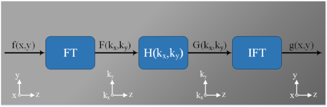
The general concept of performing mathematical operation in the spatial Fourier domain is graphically shown in Figure 2. In this figure, is the propagation direction, indicates the desired two dimensional impulse response, is an arbitrary input function and describes the corresponding output function. The whole system is assumed to be linear transversely invariant and thus the input and output functions are related to each other via the linear convolution 2:
| (1) |
Transforming eq 1 to the spatial Fourier domain leads to:
| (2) |
where , and are the Fourier transform of their counterparts in eq 1, respectively, and denotes the spatial Fourier domain variables.
For our two dimensional graphene-based system, as shown in Figure 3, the above formulation is sufficient to be presented in one dimension. In this figure and represent transverse field distribution of the incident and transmitted waves, and is the appropriate transfer function. Accordingly, eq 2 can be interpreted as:
| (3) |
where means (inverse) Fourier transform. The transfer function is given in the spatial Fourier domain , and, on the other hand, the incident wave is also transformed into the Fourier domain. Hence, any transfer function can be realized by properly manipulating the Fourier-transformed wave in its transverse direction 1.
Fourier transform can be carried out by a lens at its focal point. On the other hand, since realizing inverse Fourier transform with real materials is not possible, so instead of eq 3, the following relation should be used:
| (4) |
This relation can be easily obtained from the well-known formula, . Eq 4 implies that the output will be proportional to the mirror image of the desired output function 1.
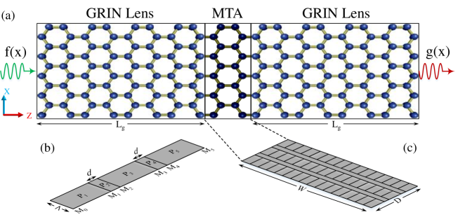
For performing Fourier transform we use graded index (GRIN) lenses. Since the optical properties of dielectric GRIN lenses change gradually, the scattering of the wave could be significantly reduced which leads to higher efficiency. To realize the graphene-based type of such lenses the surface conductivity of graphene should be properly patterned in a way that the effective mode index of GP waves follows the quadratic refractive index distribution of their dielectric counterparts 23.
GRAPHENE-BASED META-TRANSMITT-ARRAY
In this work, we implement the appropriate transfer function, by means of a new type of meta-transmit-arrays on graphene. In order to manipulate the transmitted wave efficiently, not only the transmission amplitude should be completely controlled in the range of to 24, 25, but also transmission phase should cover the whole range independently26, 27, 28. To this end, similar to the approach of Monticone et al. 4, a meta-transmit-array comprised of symmetric stack of three metalines separated by a quarter-guided wavelength transmission line is utilized (Figure 3c) in which each unit cell operates as a nanoscale spatial light modulator. To simplify the design procedure, the two outer stacks are chosen identical, but different from the inner one. The quarter-guided wavelength spacing between these stacks ensures that the transmission amplitude ripples are kept minimized 29.
In order to fully control the transmission phase, in addition to amplitude, we need to locally manipulate propagating GP waves along and across the meta-transmit-array 30. As described previously, this GP surface wave engineering is achieved via surface conductivity variation through an uneven ground plane beneath the graphene layer.
Recently, an analytical results for the reflection and transmission coefficients of GP waves at one dimensional surface conductivity discontinuity has been reported 31:
| (5) |
where
| (6) |
In these equations:
| (7) |
are the GP wavenumbers of left and right side regions of the discontinuity in the quasi-static approximation, while represent their corresponding complex surface conductivities, and is the average permittivity of the upper and lower mediums surrounding the graphene sheet. Similarly, for a GP wave incident on the discontinuity from the right side region, these coefficients, ans , can be simply achieved by exchanging and in the eqs 5, 6.
To relate the forward-backward fields on one side of the interface to those on the other side, the matching matrix is applied. By employing reciprocity theorem, the matching matrix of the interface is achieved as follows32:
| (8) |
where m=0,,5 is the interface of the building block (see Figure 3b). Furthermore, the propagative forward-backward fields relation along a segment are defined by propagation matrix 32:
| (9) |
where m=1,,5 is the segment of the unit cell. Finally, the scattering parameters can be easily calculated using the whole building block transfer matrix obtained by multiplication of the matching and propagation matrices 32:
| (10) |
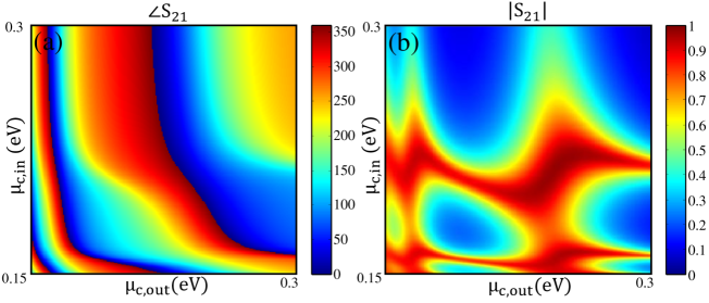
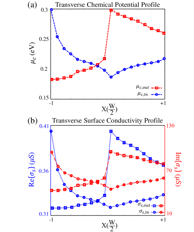
The amplitude and phase of versus the chemical potentials of the inner and outer metalines, and , are plotted in Figure 4, calculated by means of our analytical approach. It is obvious that by local tuning of the chemical potential of each unit cell any transmission phase and amplitude profile can be achieved.
IMPLEMENTAION OF MATHEMATICAL OPERATORS AND REPRESENTATIVE RESULTS
In this section, we implement first differentiation, second differentiation and integration operators, with the proposed structure. It is well-known that the derivative of a function is related to its first Fourier transform by:
| (11) |
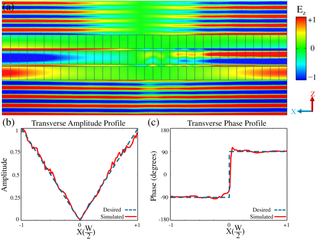
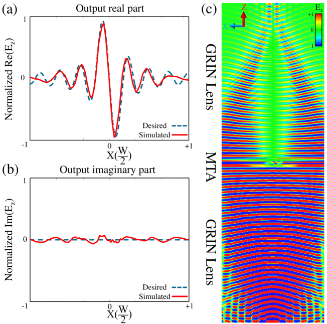
Comparing eq 3 and eq 11 clarifies that to realize the derivation we have to perform a transfer function of . So as described in the previous section we set the transfer function of the meta-transmit-array to . Since metalines are inherently passive media, the desired transfer function has to be normalized to the lateral limit to ensure that across the structure the maximum transmittance is unity, thus the appropriate transfer function is . Figures 6b,c indicate the desired magnitude and phase profile of the first-order derivative transfer function . According to Figure 4, by properly tailoring the values of the chemical potential along the lateral dimension for internal and external metalines, the transverse amplitude and phase distribution of the transfer function are implemented. To this end, the transverse distribution of chemical potential for the designed first-order differentiator meta-transmit-array and its corresponding complex surface conductivity profile are depicted in Figure 5. Now, a TM-polarized GP surface wave is launched toward the designed meta-transmit-array and the calculated electric field distribution is shown in Figure 6. As depicted in Figures 6b,c the output profile of meta-transmit-array is in an excellent agreement with the desired transfer function. To be more precise, the standard deviation from the amplitude and phase of the desired transfer function is and , respectively. This is smaller than the standard deviation observed in Fig. S7b of [1] which is about and for the amplitude and phase, respectively. As a result, a more accurate output response can be anticipated for the whole structures.
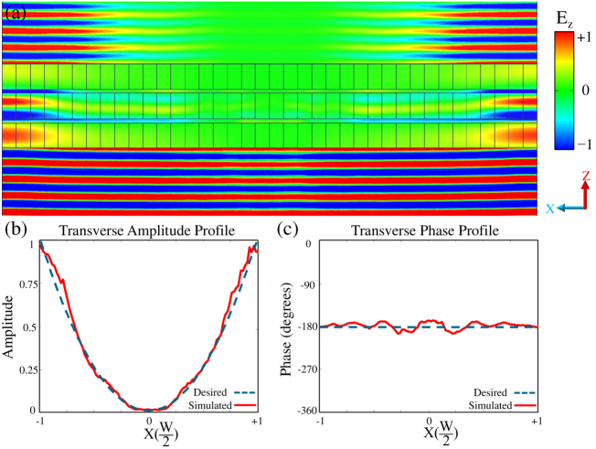
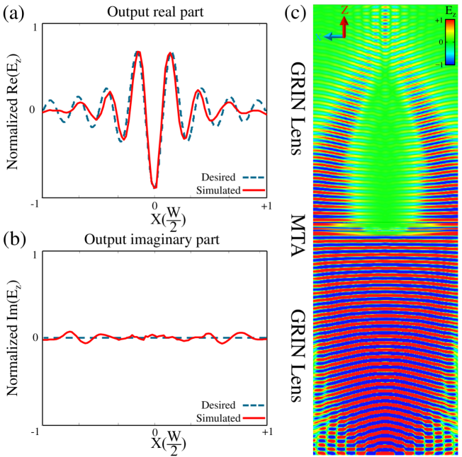
Other operators can be designed in a similar manner. In order to perform the second-order spatial derivative, the desired transfer function is . Although here the amplitude is a quadratic function of transverse dimension, the phase is constant. The results for the designed second-order differentiator are illustrated in Figure 7.
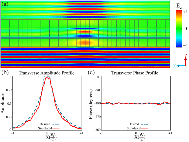
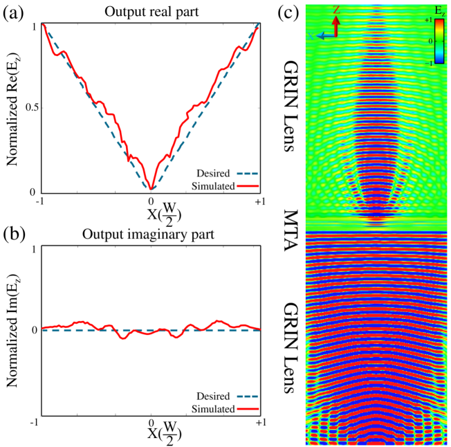
To realize a second-order integrator, a challenge should be overcome. In this case, the desirable transfer function should be which leads to an amplitude profile with values tending to infinity in the vicinity of . To overcome this problem, we use the following approximate transfer function 1:
| (12) |
where is an arbitrary parameter that we set it to 1. For all the points within the amplitude is assumed to be unity, others follow the correct transfer function profile precisely. Figure 8a shows numerical simulation of electric field distribution for this case. By comparing the obtained results from meta-transmit-array and analytical solution in Figures 8b,c , an excellent agreement is observed.
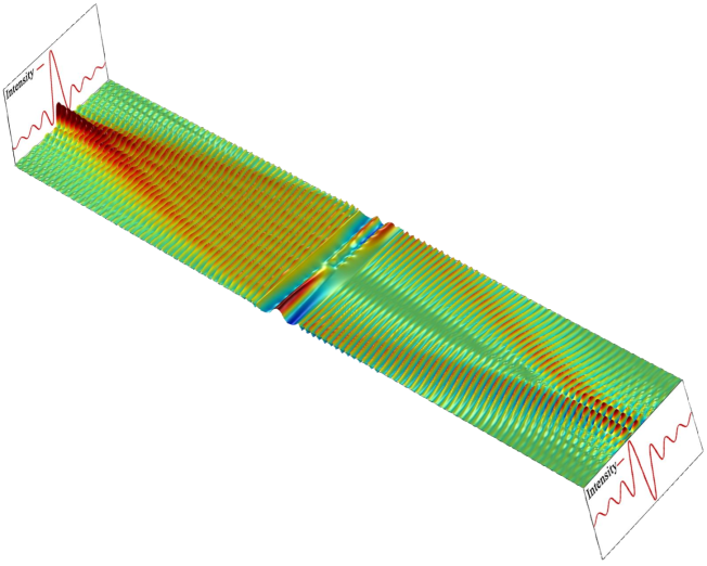
To demonstrate the functionality of our proposed structures, a GP surface wave in the form of a Sinc function is sourced into our proposed GRIN/meta-transmit-array/GRIN configuration and the simulated electric field distributions are illustrated in figures 9, 10 and 11 for the designed first-order derivative, second-order derivative and second order integrator, respectively. It is obvious from these figures that the achieved results are closely proportional to the desired results calculated analytically.
CONCLUSIONS AND OUTLOOK
In summary, we have proposed and designed a new class of planar meta-transmit-array consisting of symmetric three stacked graphene-based metalines to perform wave-based analog computing. Using analytical results for the reflection and transmission coefficients of graphene plasmon waves at one dimensional surface conductivity discontinuity 31, we have demonstrated that full control over the transmission amplitude and phase can be achieved by appropriately tailoring of surface conductivity of each building block. Employing general concept of performing mathematical operations in spatial Fourier domain, we assign the meta-transmit-array a specific transfer function corresponding to the desired operation. The two designed operators in this work; i.e. differentiator and integrator, illustrate a high efficiency. The proposed graphene-based structure not only is ultra-compact, but also depicts more accurate responses than the bulky structure suggested in [1]. These features are due to exceptionally high confinement of surface plasmons propagating on a graphene sheet. However, this miniature size comes at a price, namely any future fabrication imperfections and tolerance will lead to distortion of the anticipated results, and therefore, degrade the efficiency of the proposed structure. The presented approach may broaden horizons to achieve more complex nanoscale signal processors.
MATERIALS AND METHODS
The full-wave simulations are carried out by the commercial electromagnetic solver, Ansoft’s HFSS. Since a high confined GP wave is stimulated here, in all our numerical simulations a free standing graphene layer is assumed 15. In the simulations, the graphene layer is treated as an surface impedance , where is the complex surface conductivity of graphene can be retrieved by the Kubo’s formula under random phase approximation 33:
| (13) |
where is the angular frequency, is the chemical potential, is the relaxation time which represents loss mechanism, is the temperature, is the charge of an electron, is the reduced Planck’s constant, and is Boltzmann’s constant. In our work, K and ps, which are relevant to the recently experimental achievements34. Moreover, A time dependence of the form is assumed and suppressed throughout this study.
Due to very small mesh size, the simulation becomes computationally time consuming. As a result, we follow the approach in 3, i.e. block-by-block simulation. Initially, the first GRIN lens is excited with the desired input field profile. Then, the meta-transmit-array is excited by the monitored output field distribution of the first block. At last, the obtained output of the MTA is sourced into the second GRIN lens. To excite the GP surface wave with the desired field distribution, a current sheet is placed perpendicular to the graphene layer. By discretizing the current sheet to sufficient number of segments and assigning desired surface current amplitude and phase to them, each segment acts as an independent source. Consequently, any exact field distribution can be achieved easily.
The schematic model used in the simulations is shown in Figure 3 which contains two GRIN lenses and the meta-transmit-array embedded between them. The whole structure is restricted in transversal and longitudinal directions by and , respectively. Here, we set nm, nm, nm, nm, nm. In all simulated examples, the wavelength is chosen m. The proposed configuration can principally be implemented for other wavelengths using well-designed constituent parameters and dimensions, as long as the graphene layer supports the GP waves at that wavelength. A -polarized GP surface wave with spatial variation is used as the input function to evaluate the efficiency of the whole GRIN Lens/MTA/GRIN Lens structure. 5
References
- Silva et al. 2014 Silva, A.; Monticone, F.; Castaldi, G.; Galdi, V.; Alù, A.; Engheta, N. Performing mathematical operations with metamaterials. Science 2014, 343, 160–163
- Pors et al. 2015 Pors, A.; Nielsen, M. G.; Bozhevolnyi, S. I. Analog computing using reflective plasmonic metasurfaces. Nano letters 2015,
- Farmahini-Farahani et al. 2013 Farmahini-Farahani, M.; Cheng, J.; Mosallaei, H. Metasurfaces nanoantennas for light processing. JOSA B 2013, 30, 2365–2370
- Monticone et al. 2013 Monticone, F.; Estakhri, N. M.; Alù, A. Full control of nanoscale optical transmission with a composite metascreen. Physical Review Letters 2013, 110, 203903
- Engheta and Ziolkowski 2006 Engheta, N.; Ziolkowski, R. W. Metamaterials: physics and engineering explorations; John Wiley & Sons, 2006
- Smith et al. 2004 Smith, D. R.; Pendry, J. B.; Wiltshire, M. C. Metamaterials and negative refractive index. Science 2004, 305, 788–792
- Shalaev 2007 Shalaev, V. M. Optical negative-index metamaterials. Nature photonics 2007, 1, 41–48
- Monticone and Alu 2014 Monticone, F.; Alu, A. Metamaterials and plasmonics: From nanoparticles to nanoantenna arrays, metasurfaces, and metamaterials. Chin. Phys. B 2014, 23, 047809
- Della Giovampaola and Engheta 2014 Della Giovampaola, C.; Engheta, N. Digital metamaterials. Nature materials 2014, 13, 1115–1121
- Kildishev et al. 2013 Kildishev, A. V.; Boltasseva, A.; Shalaev, V. M. Planar photonics with metasurfaces. Science 2013, 339, 1232009
- Zhao and Alù 2011 Zhao, Y.; Alù, A. Manipulating light polarization with ultrathin plasmonic metasurfaces. Physical Review B 2011, 84, 205428
- Aieta et al. 2012 Aieta, F.; Genevet, P.; Kats, M. A.; Yu, N.; Blanchard, R.; Gaburro, Z.; Capasso, F. Aberration-free ultrathin flat lenses and axicons at telecom wavelengths based on plasmonic metasurfaces. Nano letters 2012, 12, 4932–4936
- Saeidi and van der Weide 2014 Saeidi, C.; van der Weide, D. Wideband plasmonic focusing metasurfaces. Applied Physics Letters 2014, 105, 053107
- Saeidi and van der Weide 2015 Saeidi, C.; van der Weide, D. A figure of merit for focusing metasurfaces. Applied Physics Letters 2015, 106, 113110
- Vakil and Engheta 2011 Vakil, A.; Engheta, N. Transformation optics using graphene. Science 2011, 332, 1291–1294
- Vakil and Engheta 2012 Vakil, A.; Engheta, N. Fourier optics on graphene. Physical Review B 2012, 85, 075434
- Tymchenko et al. 2013 Tymchenko, M.; Nikitin, A. Y.; Martin-Moreno, L. Faraday rotation due to excitation of magnetoplasmons in graphene microribbons. ACS nano 2013, 7, 9780–9787
- Koppens et al. 2011 Koppens, F. H.; Chang, D. E.; Garcia de Abajo, F. J. Graphene plasmonics: a platform for strong light–matter interactions. Nano letters 2011, 11, 3370–3377
- Bao and Loh 2012 Bao, Q.; Loh, K. P. Graphene photonics, plasmonics, and broadband optoelectronic devices. ACS nano 2012, 6, 3677–3694
- Lu et al. 2013 Lu, W. B.; Zhu, W.; Xu, H. J.; Ni, Z. H.; Dong, Z. G.; Cui, T. J. Flexible transformation plasmonics using graphene. Optics express 2013, 21, 10475–10482
- Chen and Alù 2011 Chen, P.-Y.; Alù, A. Atomically thin surface cloak using graphene monolayers. ACS nano 2011, 5, 5855–5863
- Fallahi and Perruisseau-Carrier 2012 Fallahi, A.; Perruisseau-Carrier, J. Design of tunable biperiodic graphene metasurfaces. Physical Review B 2012, 86, 195408
- Wang et al. 2014 Wang, G.; Liu, X.; Lu, H.; Zeng, C. Graphene plasmonic lens for manipulating energy flow. Scientific reports 2014, 4
- Pfeiffer and Grbic 2013 Pfeiffer, C.; Grbic, A. Cascaded metasurfaces for complete phase and polarization control. Applied Physics Letters 2013, 102, 231116
- Pfeiffer et al. 2014 Pfeiffer, C.; Emani, N. K.; Shaltout, A. M.; Boltasseva, A.; Shalaev, V. M.; Grbic, A. Efficient light bending with isotropic metamaterial Huygens’ surfaces. Nano letters 2014, 14, 2491–2497
- Cheng and Mosallaei 2014 Cheng, J.; Mosallaei, H. Optical metasurfaces for beam scanning in space. Optics letters 2014, 39, 2719–2722
- Pors et al. 2013 Pors, A.; Albrektsen, O.; Radko, I. P.; Bozhevolnyi, S. I. Gap plasmon-based metasurfaces for total control of reflected light. Scientific reports 2013, 3
- Pors and Bozhevolnyi 2013 Pors, A.; Bozhevolnyi, S. I. Plasmonic metasurfaces for efficient phase control in reflection. Optics express 2013, 21, 27438–27451
- Lau and Hum 2012 Lau, J. Y.; Hum, S. V. Reconfigurable transmitarray design approaches for beamforming applications. Antennas and Propagation, IEEE Transactions on 2012, 60, 5679–5689
- Zentgraf et al. 2011 Zentgraf, T.; Liu, Y.; Mikkelsen, M. H.; Valentine, J.; Zhang, X. Plasmonic luneburg and eaton lenses. Nature nanotechnology 2011, 6, 151–155
- Rejaei and Khavasi 2015 Rejaei, B.; Khavasi, A. Scattering of surface plasmons on graphene by a discontinuity in surface conductivity. Journal of Optics 2015, 17, 075002
- Orfanidis 2002 Orfanidis, S. J. Electromagnetic waves and antennas; Rutgers University New Brunswick, NJ, 2002
- Hadad et al. 2014 Hadad, Y.; Davoyan, A. R.; Engheta, N.; Steinberg, B. Z. Extreme and quantized magneto-optics with graphene meta-atoms and metasurfaces. ACS Photonics 2014, 1, 1068–1073
- Shen 2015 Shen, N.-H. Tunable terahertz meta-surface with graphene cut wires. ACS Photonics 2015,