Miscut dependent surface evolution in the process of N-polar GaN growth under N-rich condition
Abstract
The evolution of surface morphology during the growth of N-polar GaN under N-rich condition is studied by kinetic Monte Carlo (kMC) simulations for two substrates miscuts and . The results are compared with experimentally observed surface morphologies of GaN layers grown by plasma-assisted molecular beam epitaxy. The proposed kMC two-component model of GaN surface where both types of atoms: nitrogen and gallium attach the surface and diffuse independently, explains that at relatively high rates of the step flow (miscut angle <) the low diffusion of gallium adatoms causes surface instabilities and leads to experimentally observed roughening while for low rates of the step flow (miscut ), smooth surface can be obtained. In the presence of almost immobile nitrogen atoms under N-rich conditions, the growth is realized by the process of two-dimensional island nucleation and coalescence. Additionally, we show that higher crystal miscut, lower crystal growth rate or higher temperature results in similar effect of the smoothening of the surface. We show that the surface also smoothens for the growth conditions with very high N-excess. The presence of large number of nitrogen atoms changes locally mobility of gallium atoms thus providing easier coalescence of separated island.
keywords:
American Chemical Society, LaTeXFaculty of Mathematics and Natural Sciences, Card. Stefan Wyszynski University, ul. Dewajtis 5, 01-815 Warsaw, Poland \abbreviationsIR,NMR,UV
![[Uncaptioned image]](/html/1509.01035/assets/toc.png)
1 Introduction
The fact that in wurtzite N-polar GaN, the direction of the polarization fields is reversed compared to the Ga-polar direction, makes the N-polar GaN of interest for a variety of device applications such as high electron mobility transistors, solar cells, sensors and light emitting diodes 1, 2, 3. Identification of the optimum growth conditions providing smooth surface morphology N-polar GaN is one of the key issues to enhance the development of these emerging applications. The growth of atomically flat N-polar GaN layers by plasma-assisted molecular beam epitaxy (PAMBE) has been proven difficult due to the high adatom diffusion barriers because it is carried out at relatively low temperatures . Theoretical works showed that these diffusion barriers are substantially reduced when gallium adlayer is present on the surface during the growth 4, 5, 6, 7. However, previous experimental studies showed that the growth of the N-face GaN must be performed with less than one monolayer (ML) of excess Ga on the growing surface, in contrast to Ga-polarity, when more than 2ML can be stabilized. Therefore, a precise control of the growth conditions is needed to prevent the accumulation of Ga droplets8. The morphologies reported for N-polar GaN layers grown by PAMBE under N-rich conditions on low miscut substrates were relatively rough either due to the hillocks or pattern formed by interlacing stripes covered by doubly-bunched atomic steps 9. In search for the optimum growth conditions of the device-quality N-polar GaN layers it is essential to understand of the role of surface miscut, growth temperature, growth rate and III/V ratio (N-excess) that may improve surface morphology. It is important to note that in case of metal-organic vapor phase epitaxy (MOCVD), the N-polar GaN films for many years suffered from high surface roughness resulting from the formation of large hexagonal hillocks10. The use of 4 deg miscut N-polar GaN substrates has proven to be effective method of improving surface morphology 3.
In this work the growth of N-polar GaN surface under N-rich conditions is investigated theoretically by kinetic Monte Carlo (kMC) simulations and compared to experimental results in order to identify the optimum growth conditions leading to smooth layer morphologies and understand the role of substrate miscut, temperature, growth rate and N-excess. We built two-component model of GaN surface. We use the model that is based on the one previously implemented to study growth and sublimation of GaN(0001) surface 11, 12, 13, 14. The model is developed in such a way that both types of atoms building crystal: nitrogen and gallium are controlled. They attach to the surface, diffuse and detach independently. They can be adsorbed at the steps or form islands by nucleation at the terraces. In this work we study the influence of substrate miscut on the morphology of GaN layers by comparing the simulated systems to the morphologies of N-polar GaN layers grown bt PAMBE under N-rich conditions.
In our kMC simulations of N-polar GaN growth under N-rich conditions we apply 1eV barrier for Ga surface diffusion as evaluated in ab-initio calculations 4 and 1.8eV high barrier for diffusion of N adatoms. With such a slow surface dynamics we model the crystal growth under large nitrogen flux at relatively high miscuts. We choose external fluxes and desorption rates in such a way that simulations follow experimental crystal growth rates. As a result the experimentally observed morphology patterns are well reproduced. We explain that the surface instability appears due to the too slow diffusion of gallium atoms at relatively high flux of incoming atoms and because of the wide terraces as compared to the diffusion length of Ga adatoms15, 17, 16, 18. However if steps are located more densely, crystal surface becomes smoother under the same growth conditions. In two component system of GaN, at miscut of 4o, diffusion rate of N adatoms is below and of Ga adatoms close to the limiting value for the domain formation on the terrace 17, 16, 18, 20, 21, 19. If the diffusing particle has enough time to find a step edge before the next one attaches to it the island nucleation process is suppressed. When this condition is fulfilled we observe smooth crystal growth realized either by step flow or mixed made of step flow and two dimensional nucleation process 22. It is interesting that we observe such growth mode for two component system, when one component is slower and the second moves with rate close to the expected limiting diffusion value. This limiting value can be decreased by higher surface miscut, lower crystal growth rate or higher temperature. Our kMC simulations confirmed that all these methods lead to lower surface roughness. Thus we can explain experimentally observed differences in surface morphologies of N-polar GaN grown at and surface miscuts. However, due to heterogeneous growth and immobility of nitrogen adatoms the character of stable and unstable surface evolution is a mixture of step flow and 2-D or 3-D island growth 16, 18, 17, 19.
We find that low miscut angle results in characteristic surface instabilities (and subsequent high surface roughness), while for steeper cuts a smooth double-step surface pattern is observed. Other methods of surface smoothening lead to slightly different surface morphologies. For instance higher temperature smoothens the surface, but contrary to the high miscut case no double step structure can be seen. Distances between all steps are equal suggesting that at higher temperature all steps move with the same rate at low external particle flux (slow crystal growth rate). The resulting surface morphology is very similar to this for cut crystal. It can be seen when appropriate correlation functions are compared. However there are some differences in both patterns that suggest that dynamics of the process is slightly different.
We have found that step roughness can be smoothened also using increased nitrogen flux. As nitrogen practically does not move along the surface at studied temperatures and the rate of gallium adatoms diffusion is also below limiting value, the character of this process is different than that studied above. The pattern that builds at the surface consists of islands that grow along step-edges and finally attach to the step. Resulting smooth crystal growth is realized by two dimensional island nucleation. We show that a flat surface is developed at relatively low miscut at high nitrogen rates. We discuss numerical data as a function of the growth temperature, growth rate defined by Ga flux and substrate miscut angle. The kMC results are compared with experimental data.
First in Section II the model is formulated, then in Section III we show how the surface structure changes with miscut, temperature, galium and nitrogen flux. Surface patterns obtained for the chosen parameters are compared to the experimental data. Finally on the basis of the surface dependence on the nitrogen flux we consider possibility of the surface smoothening via use of higher nitrogen fluxes.
2 Kinetic Monte Carlo model
Numerical simulations of the system were performed with use of two-component kMC model. It consists of gallium and nitrogen atoms arranged in a crystallographic lattice of N-face of gallium nitride. Two species interact via nearest neighbor (NN) and next nearest neighbor (NNN) forces which form N-N, Ga-Ga, and Ga-N bonds. Total energy of an adatom occupying one of the lattice sites is given by the sum over all NNs and NNNs surrounding it
| (1) |
where X corresponds to Ga or N atom and the value depends on the state of the neighboring site. If the site is occupied otherwise . Energies associated with interactions are , and respectively. They were chosen in such a way that total energy of Ga atom built in the crystal is 10.6 eV. This value is in agreement with molecular dynamic calculations performed by Wang et. al 23 using a bond order potential.
Single simulation consists of several Monte Carlo (MC) steps. Each of them starts with particle adsorption which occurs with probability equal to the external flux F. Adsorbed particles are allowed to diffuse at the surface. That process is modeled in three stages. At first one of the neighboring sites is randomly chosen to be the target of a jumping particle. Next initial () and final () energies of jumping atom are calculated using eq. (1). In the third stage of diffusion process particles jump with probabilities:
where and sets the time scale. denotes the diffusion barrier that is different for =Ga, N adatoms. It is known that diffusion barriers for both components under nitrogen rich conditions on GaN surface are high4, 5, 6, 7. We use barriers calculated in Ref. 4, and so Ga adatoms diffuse jumping over the barrier and N adatoms jump over barrier . According to the Eq. 2 particle, which is strongly binded in its initial state, resides in a deep potential well and probability of the jump out is low. However when final state has low energy i.e. particle tries to move to the deep well the energy barrier between these states decreases and jump rate is high. Finally jumps towards step from above occur with the same probability like those far from the step in such a way that effectively no additional barrier for jumps across step (Schwoebel barrier) is present in the studied systems. During the last stage of a single MC step, the evaporation phenomenon is simulated. An assumption that incoming atoms can evaporate is necessary in order to reach equal number of Ga and N atoms within the growing crystal. We set the following rate of particle desorption:
| (2) |
where is the desorption potential, different for Ga and N adatoms. We set taking into account that binding energy of single N atom at the surface =5.7eV while the same atom above the GaN surface covered by nitrogen . This value of desorption barrier ensures that most of N adatoms that are not bonded to gallium atoms in the layer below, desorb from the surface, whereas the ones that have fallen onto the gallium layer stick to the surface. For gallium we set . Such choice of desorption potentials provides that the number of adsorbed atoms of both types equalizes at the surface. After evaporation stage new MC step begins and the above procedure starts from the beginning.
At the beginning of each simulated process, the system consists of straight steps. Helical boundary conditions in one direction and periodic in the second one are posed. Gallium nitride elementary cell consists of four mono-atomic layers, hence in order to close helical boundary condition properly, is always divisible by 4. Additionally, because N-rich conditions are studied, we start the simulation with total N coverage of the surface, what changes during the growth process by evaporation of adatoms from the surface.
Summarize, the kMC model used to describe N-polar GaN() growth under N-rich conditions we build of two types of atoms: Ga adatoms that move slowly but are able to diffuse across terraces and reach steps, and N adatoms that are almost immobile, but can desorb from the surface and are frequently adsorbed because of the relatively high flux of N atoms. The consequence of such assumptions is that both atomic monolayers (nitrogen and gallium) can grow smoothly within some range of parameters, but due to totally different mechanisms. Gallium adatoms diffuse over the surface, and they start to build islands when incoming flux is too high, whereas nitrogen adatoms being practically immobile build islands all the time. Nitrogen islands have two different roles in the growth process: they build in the step thus completing the layer formation, but they also change diffusion of Ga adatoms. Below we analyze consequences of such adatom dynamics for the evolution of stepped surfaces.
3 MBE experimental details
In parallel we carried out the growth of 200nm thick N-polar GaN layers by PAMBE custom design Gen20A MBE reactor were active nitrogen was supplied from Veeco RF plasma source. We used bulk, commercially available GaN substrates from Saint Gobain with threading dislocation density around 5 x 107 cm-2. Prior to growth, substrates were mechanically polished to get miscut angle of and toward direction and chemomechanically polished to obtain atomically smooth surface. Epi-ready substrates were then mounted by gallium to single 2 inch wafer close to its center to ensure the same growth conditions at both crystals. Growth of 200 nm thick GaN was carried out at out under nitrogen rich conditions using nitrogen and gallium fluxes of and (GaN equivalent growth rate) respectively. After the growth samples morphology was examined by atomic force microscope (AFM).
4 Dependence of the surface ordering on the growth parameters
4.1 Miscut
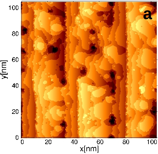
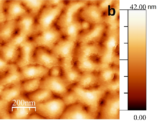
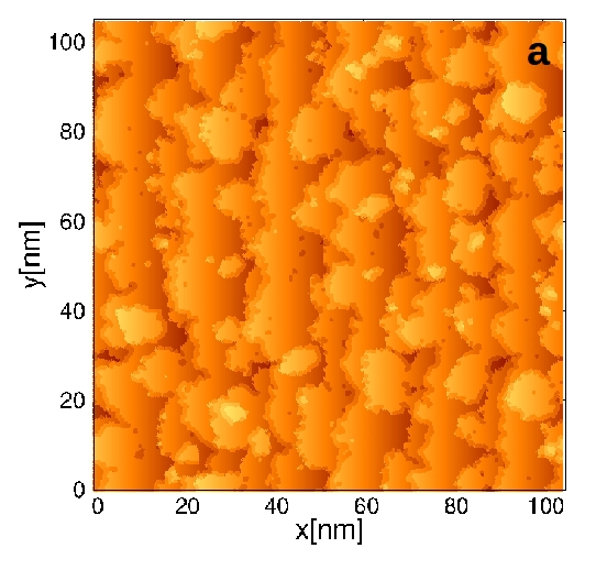
1 presents the numerical (a) and experimental (b) results of N-polar GaN layer morphology for the case of miscut surface. For both cases (experimental and calculations) growth parameters like temperature and atomic fluxes were the same. The size of calculated system is 105 nm 105 nm, smaller than the area of AFM scan which is m m. Despite this it can be seen that in both cases crystal does not grow smoothly. In 1a several cavities can be easily seen, steps bend and become wavy leaving deep cavities on their way forward. In the process of further growth more profound structures can build around them. In 1b we can see that the surface is rough, dominated by islands. This is typical pattern expected for systems with slow adatom diffusion.
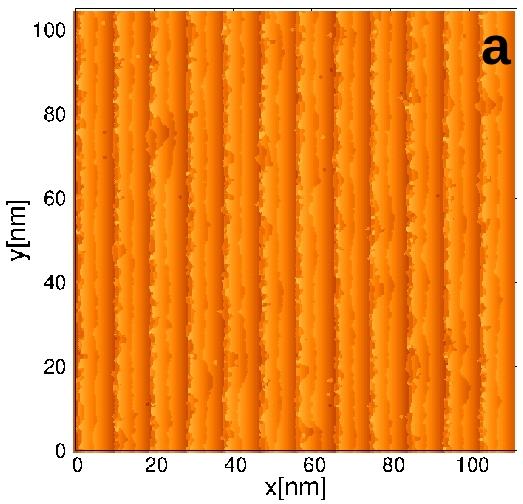
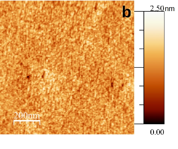
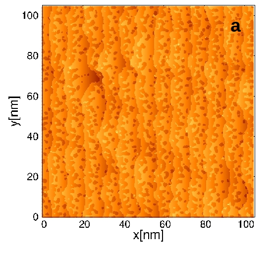
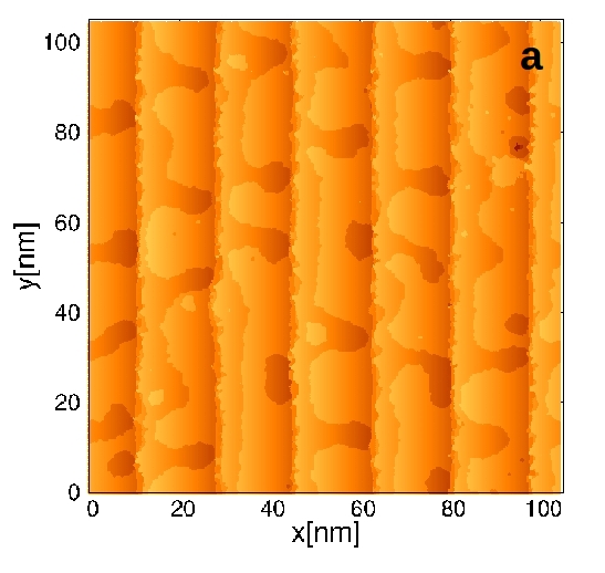
The situation changes diametrically when growth is performed under the same conditions (impinging fluxes and temperature), but at the substrate cut . 2a presents the simulated surface pattern for miscut. Double-steps with relatively straight edges are seen. 2b presents the AFM scan of N-polar GaN layer grown by PAMBE. We can see smooth, stepped surface. The double step structure however is not so clearly visible like in the simulated plot above. The double step structure is a consequence of GaN lattice geometry according to which every second step perpendicular to [100] direction has different bond arrangement. Thus the rate of adatom adsorption at the step and resulting velocity of every second step is different.
In order to analyze and compare surface parameters more precisely we have calculated root mean square (RMS) roughness
| (3) |
where is the z coordinate (height) of i-th site over leveled surface and is mean system height. RMS parameters for numerical results presented in 1a and 2a are 0.38nm and 0.15nm respectively. The same parameters calculated for corresponding experimental data (1b and 2b) are 6.11nm and 0.49nm. Roughness measured for experimental surfaces is obviously higher due to the surface distortion or local defects, however one can notice that RMS parameters for lower miscut are higher both in the experiment and simulations as well. Numerically obtained surfaces are smoother also due to the shorter time of system evolution, which for experiments was about 40 minutes and 2-3 minutes for simulations as well as due to different size of the surface area.
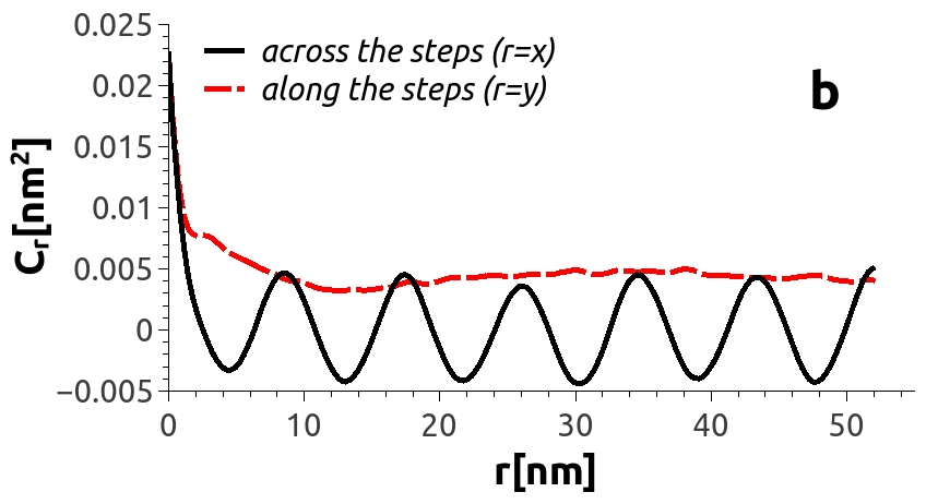
In order to illustrate and analyze surface features, in particular their periodicity and amplitude we calculated correlation functions along and across steps according to the formula:
| (4) |
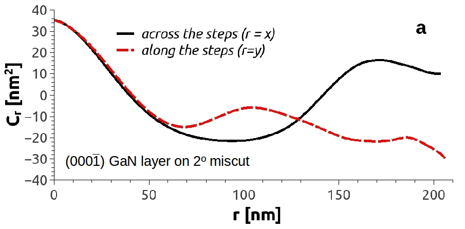
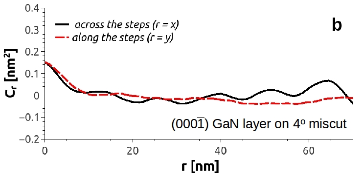
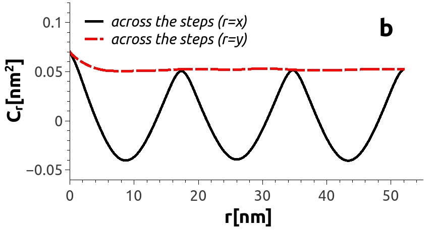
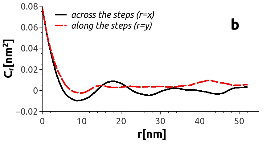
where the difference in position is calculated along x or y axis i.e. across () or along () steps. 3 presents the correlation functions calculated for experimentally measured surface morphology of N-polar GaN layers grown by PAMBE on (a) miscut and (b) micut GaN substrate. We can see that the scale of variability of the curve is much larger than that for surface i.e. vs. respectively. 3a. shows that the correlation function calculated for the surface of oscillates in both directions. The length scale of its changes along and across steps is much longer than bilayer step distance (20nm). We can see that the characteristic correlation length is shorter across than along steps. The correlation function across steps of miscut surface (3b) shows periodicity of around 10 nm length denoting bi-step surface structure. The function along step is flat and close to zero describing smooth surface.
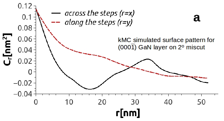
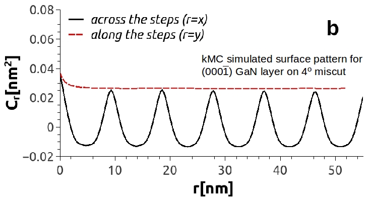
Correlation functions for simulated GaN surfaces on miscut (4a) and 4o miscut (4b) exhibit many similarities to the experimentally corresponding counterparts. The characteristic length scales at cut are shorter in both directions, thought it reflects less corrugated structure due to short available simulation times. Nevertheless the period of correlation function oscillations is still longer than bilayer step distance. Correlation function across the steps for miscut , presented in 4b, clearly shows the step structure. Oscillations of the function are very regular and all with the same amplitude what corresponds to the very regular structure. Thus the character of surface morphology is very well reflected by the shape of correlation function.
The analysis of the correlation function for the GaN surface morphologies obtained on miscut and miscut substrates confirms that the surface of a crystal grown at substrate with higher miscut is more regular then the surface which evolved at the substrate with lower miscut. In order to understand the causes of observed differences we carry out the following analysis: Formation of Ga 2D islands on the terraces is probable for miscut because the average diffusion length for Ga adatoms until they meet next particle is around 8nm, which is close to the terrace width for 2o cut. To be more precise we calculate the limit terrace length for the domain formation 17, 18, 19, 20, 21, that is given by the relation . For our data, due to the low diffusion barrier, the limit terrace length is around for nitrogen adatoms and for gallium adatoms, where denotes GaN lattice constant , This gives and as compared with the terrace width at the surface of miscut and in the case. This means that in this for miscut GaN surface nitrogen adatoms have tendency of creating islands, whereas gallium adatoms are at the crossover length. However at the temperatures studied the surface has a tendency to build bi-layer structures. Hence terrace width that has to be considered as being two times wider. As a result adatoms at miscut surface are already within the crossover region.
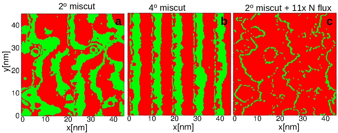
In such situation, particles adsorbed at the steeper surface start to form islands, but because these islands built up short distance to step edges. Steps move forward due to the attachment of other particles. In such a way islands are absorbed at the steps . It can be seen in 5b. Green points that are plotted for gallium atoms are arranged in pattern that looks like many islands glued together. Nitrogen adatoms seem to have not much importance here, because there are enough of them all around. Hence the system forms steps straight and distributed regularly in space. On the other hand, when miscut angle is low, terraces are wider and particles need more time to reach the step. In such case the probability of 2-dimensional nucleation is higher. As a result of this process islands would appear at terraces. They are partly adsorbed by steps, leaving some cavities beside them and irregular wavy pattern builds up (5a). Less mobile nitrogen adatoms that are adsorbed and desorbed seem to play a role in building 3D islands. On building next layer on top of island they can be source of effective Schwoebel barrier for wandering gallium adatoms. For much higher nitrogen flux this reasoning does not work. Nitrogen adatoms are everywhere and they are rather smoothening the surface of growing crystal as we can see in 5c.
4.2 Temperature
Higher miscut successfully flattens the surface by shortening the time that adatom needs to reach the step. Knowing that we carried out another simulation for miscut applying a higher growth temperature, thus increasing surface diffusion rate to check if this will result in smoother surface. In 6 we show simulated surface morphology for GaN layer on miscut surface obtained at the temperature , that is higher than the reference (cf. Fig 1). In such case diffusion is 4 times faster than in the reference example. It should compensate 4 times longer lasting diffusive walk, what means effectively 2 times longer terrace width. Comparing the surface morphologies in Fig. 1a and Fig. 6a we see the positive effect of raised temperature on the surface smoothness. Calculated RMS value for the N-polar GaN surface simulated at 850 is , what is low value. However the morphologies obtained at raised temperature on miscut substrate (6) and at reference temperature on miscut GaN substrate are different. As can be concluded from the correlation functions, plotted in Fig. 4b and 6b. Regular pattern across steps is clearly visible, but with no sign of double step structure. In 6b the periodicity of the correlation function is around 10nm across the steps, while along the steps nice smooth terraces are indicated by low, close to zero correlation line. Such structure can be also seen in Fig. 4b. However, when we look closer at the surface morphology in Fig. 6 we can see that every second step has irregular structure similar to that seen in Fig. 5b. More detailed study shows that these island-like structures are build by nitrogen and not by gallium atoms. Gallium steps at the other side have tendency to bend at characteristic length related to the diffusive distance at given temperature.
4.3 Growth rate
The other method of surface smoothening is to use a lower flux of incoming particles i.e. lower growth rate. In such a way diffusing adatom has more time to wander around on the surface and as a result the steps should become more straight. In 7a we see an effect of the slow growth rate (flux are 4 times slower than in the reference surface in 1). Again we can see a rather smooth surface. It differs from this obtained by increased temperature. We can see bi-step structure, like in the case of miscut. Such structure is reflected in the shape of the correlation functions presented in 7b. Correlation in the direction perpendicular to steps is very similar to this in 2, but in two times larger distance scale. At the same time correlation along step quickly decreases to zero. is higher than in the case of surface of crystal grown at higher temperature 6.
4.4 N-excess
One more simulation was carried out to study the effect of the increased nitrogen flux on surface morpholog. In 8a we show the surface of GaN on miscut obtained under the growth conditions of high N excess, i.e. the flux of incoming nitrogen is 30 times higher than gallium flux. Part of this surface was already presented above in 5c. It can be seen that the surface is much smoother that this in 2, however not in the same manner as miscut case as seen in the simulated system in 2a. It is easy to note that the increase of nitrogen amount in the system leads to the improvement of surface quality. There are no cavities seen in 8 and the height differences are not so large as in the reference GaN surface. However, the overall surface structure is not so regular as in the cases studied before. The calculated value of is lower than the reference miscut GaN layer. When we look at the correlation function along steps presented in 8b we see that it decreases very quickly, like for smooth structures. The correlation function across the steps shows oscillations of characteristic length for double step structure i.e. 20nm.
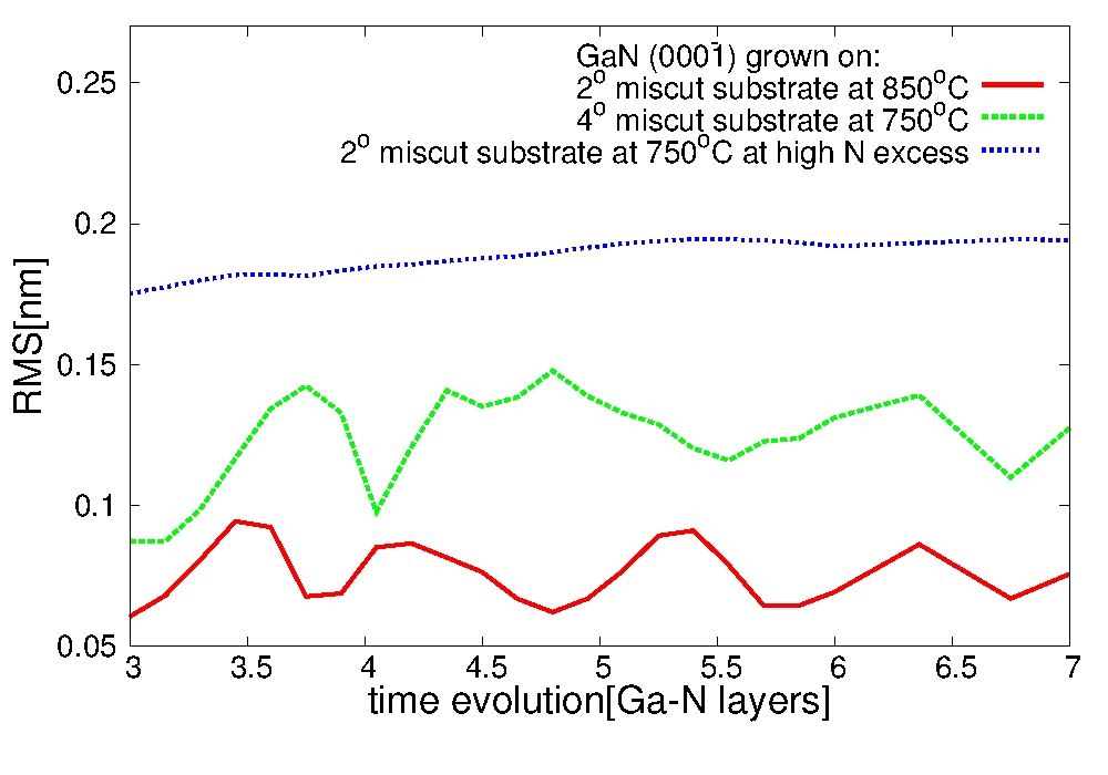
In the last part of our study we analyzed the evolution of surface RMS parameter as a function of surface coverage, counted in the numbers of grown layers for three cases of GaN growth: high miscut, high temperature, and high N flux. The result is shown in Fig. 9. For the case of layer grown at the miscut GaN substrate and high temperature miscut growth process is evidently periodic. One can see oscillations in RMS when the growth proceeds. It can be interpreted as layer by layer growth via creation of islands, than absorption of these islands by approaching steps, and the cycle ends up by next layer to be completed 24, 25. We can clearly see periodicity of the length of one monolayer in the plotted curves. Typically, the higher temperature process is the smoother line we would expect, but it has the same period related to the number of layers. Third curve is plotted for high N-excess case RMS value stays at the same, relatively high level, showing that the growth process is realized in a different way. We attribute it to the island formation and coalescence that results in a stable RMS value over the growth time.
5 Conclusions
Kinetic Monte Carlo simulations have been employed to study the surface evolution of N-polar GaN layers grown on the substrates of and miscut. The numerical results are compared with experimentally observed surface morphologies of GaN layers grown by MBE. Due to the high diffusion barriers during the growth of GaN under N-rich conditions the resulting surface is irregular and rough. Such surface can be observed for the crystal grown at surface miscut at temperature around 750oC. Four different methods of smoothening the surface were investigated using kinetic Monte Carlo method: (a) growth of GaN on high misut substrates, (b) at higher temperature, (c) at low growth rate and (d) using high N-excess. All of them lead to smoother crystal surfaces. The surface of cut seems to be the most regular one, that has been also confirmed by by experimental results. Other approaches like: higher temperature or lower growth rate have also work as smoothening factor, but the character of the surface morphology is different than this for the high miscut surface. Their further evolution seems to happen less smoothly due to meandering steps and nucleation on terraces that lead to the formation of cavities. The surface that emerged during the growth at high N-excess using very high nitrogen flux is quite unusual, because microscopically it seems to be irregular, but correlation functions exhibit rather regular structure. Thus, we conclude that under high N-excess GaN growth happens regularly and the surface morphology remains smooth due to stable island formation and coalescence on the terraces. Therefore the use of high nitrogen flux for the growth of GaN under N-rich conditions seems to be a good method to obtain smooth surface morphology.
Research supported by the National Science Centre(NCN) of Poland (Grant NCN No. 2013/11/D/ST3/02700)
References
- 1 S. Rajan, A. Chini, M. H. Wong, J. S. Speck, and U. M. Mishra, J. Appl. Phys., 102, 044501, 2007.
- 2 W. M. Hoi, K. Stacia, S. D. Nidhi, D. D. J., K. Seshadri, F. B. David, L. Jing, F. N. A., A. Elaheh, S. Uttam, C. Alessandro, R. Siddharth, P. D. Steven, S. James, M. K. Umesh, Semiconductor Science and Technology, 28 074009 (2013).
- 3 S. Keller, H. Li, M. Laurent, Y. Hu, N. Pfaff, J. Lu, D. F. Brown, N. A. Fichtenbaum, J. S. Speck, S. P. DenBaars, U. K. Mishra, , Semiconductor Science and Technology, 29 113001 (2014).
- 4 T. Zywietz, J. Neugebauer, M. Scheffler Appl. Phys. Lett. 73, 487 (1998).
- 5 J. Neugebauer et al., Physical Review Letters 90, 056101 (2003).
- 6 N. Takeuchi, A. Selloni, T. H. Myers, and A. Doolittle, Phys. Rev B 72,115307 (2005).
- 7 R. M. Feenstra, J. E. Northrup and J. Neugebauer, MRS Internet J. Nitride Semicond. Res. 7, 3 (2002).
- 8 E. Monroy, E. Sarigiannidou, F. Fossard, N. Gogneau, E. Bellet-Amalric, J.-L. Rouvière, S. Monnoye, H. Mank, B. Daudin, Applied Physics Letters, 84 3684 (2004).
- 9 C. Chèze, M. Sawicka, M. Siekacz, H. Turski, G. Cywinski, J. Smalc-Koziorowska, J. L. Weyher, M. Kryśko, B. Lucznik, M. Bockowski, C. Skierbiszewski et al., Applied Physics Letters 103, 071601 (2013).
- 10 A. R. A. Zauner, J. L. Weyher, M. Plomp, V. Kirilyuk, I. Grzegory, W. J. P. van Enckevort, J. J. Schermer, P. R. Hageman, P. K. Larsen, Journal of Crystal Growth, 210 435 (2000).
- 11 M. A. Załuska-Kotur, F. Krzyżewski, S. Krukowski, Michał Leszczynski, Robert Czernecki Cryst. Growth and Design 13, 1006 (2013).
- 12 M. A. Załuska-Kotur, F. Krzyżewski, S. Krukowski, Journal of Applied Physics, 109 023515 (2011).
- 13 M. A. Załuska-Kotur, F. Krzyżewski, Journal of Applied Physics 111, 114311 (2012).
- 14 M. A. Załuska-Kotur, F. Krzyżewski, S. Krukowski, J. Cryst. Growth 343 138 (2012).
- 15 C. Misbah, O. Pierre-Louis, and Y. Saito, Rev. Mod. Phys. 82, 981 (2010).
- 16 H.-C. Jeong, E. D. Williams, Surf. Sci. Rep. 34, 171 (1999)
- 17 P. Politi, G. Grenet, A. Marty, A. Ponchet, J. Villain,Physics Reports 324 (2000) 271
- 18 Jacques Villain ,Alberto Pimpinelli, Leihan Tang and Dietrich Wolf, J. Phys. I France 2 2107 (1992).
- 19 J. W. Evans, P. A. Thiel, M. C. Bartelt, Surface Science Reports 61, 1 (2006).
- 20 G. B. Stephenson, J. A. Eastman, C. Thompson, O. Auciello, and L. J. Thompson, Appl. Phys. Lett., 74, 3326 (1999).
- 21 Edith Perret, M. J. Highland, G. B. Stephenson, S. K. Streiffer, P. Zapol, P. H. Fuoss, A. Munkholm, and C. Thompson, Applied Physics Letters 105, 051602 (2014).
- 22 M. Rusanen, I. T. Koponen, and J. Kallunki, Eur. Phys. J. B, 36, 141-147 (2003).
- 23 K. Wang, J. Singh, D. Pavlidis J. Appl. Phys. 76, 3502 (1994).
- 24 R. Kunkel, B. Poelsema, L.K. Verheij, G. Comsa, Phys. Rev. Lett. 65, 733 (1990)
- 25 P. Ŝmilauer, M. R. Wilby, D. D. Vvedensky, Phys. Rev. B 47, 4119 (1993)