Instituto de Ciencia de Materiales “Nicolás Cabrera”, Campus de Cantoblanco, E-28049 Madrid, Spain \altaffiliationInstituto de Ciencia de Materiales “Nicolás Cabrera”, Campus de Cantoblanco, E-28049 Madrid, Spain \altaffiliationInstituto de Ciencia de Materiales “Nicolás Cabrera”, Campus de Cantoblanco, E-28049 Madrid, Spain \altaffiliationIKERBASQUE, Basque Foundation for Science, E-48013, Bilbao, Spain
Strain induced bang-gap engineering in layered .
Abstract
By combining ab initio calculations and experiments we demonstrate how the band gap of the transition metal tri-chalcogenide TiS3 can be modified by inducing tensile or compressive strain. We show by numerical calculations that the electronic band gap of layered TiS3 can be modified for monolayer, bilayer and bulk material by inducing either hydrostatic pressure or strain. In addition, we find that the monolayer and bilayer exhibits a transition from a direct to indirect gap when the strain is increased in the direction of easy transport. The ability to control the band gap and its nature can have an impact in the use of TiS3 for optical applications. We verify our prediction via optical absorption experiments that present a band gap increase of up to 10% upon tensile stress application along the easy transport direction.
The discovery of graphene 1 paved the way to the investigation to a vast class of materials whose salient characteristic is to exist in single or a few layers. Similar to graphene for example, the existence of silicene and germanene has been predicted 2, 3, 4. At the same time, the mechanical exfoliation technique that allowed the breakthrough for the carbon based material, going from graphite to graphene, allows to produce single (or a few) layers of other materials. A family of these materials are the transition metal dichalcogenides (TDMs) like, e.g., MoS2, MoSe2, WS2, and WSe2. TDMs have shown semiconducting properties, like a direct gap and tunability, superior to certain extent to those of graphene and could form a basis for novel transistors and photodetectors. Ideally, these materials should have a gap comparable with that of Silicon to ease the integration on the existing technology. However, TDMs show a direct gap only when reduced to a single layer, due to interlayer interaction. This might limit their systematic use. On the other hand, trichalcogenides can be reduced to single or a few layer devices while showing a direct gap of about 1 eV 5. In particular titanium trisulphide, TiS3, shows an extremely fast optical response: an ideal property for the next generation of photodetectors 6, 7, 8. Moreover, it has been predicted that TiS3 could be a promising electrode material for Li and Na in batteries 9, as photoelectrode for H2 photogeneration 10, and nano-electronics and optics 11, presenting also strong anisotropic behavior and non-linearity both in the electronic and optical properties 12, 7, 8, 13.
The exfoliation of a few layer TiS3 is a relatively recent achievement 6. It has also been shown that by controlling the growing conditions one can obtain different materials, from nano-ribbons to flakes as well as control several electrical properties of TiS3. In particular, the presence of S vacancies has an important effect on the electronic transport properties of the few layers nano-ribbons 7, 14. In this Letter we show that one can control the electronic band gap by inducing compressive and expansive uniaxial strain or hydrostatic pressure to the material. Here, we consider the cases of bulk, mono- and bi-layer devices, and show that one can induce a direct-to-indirect band-gap transition by inducing strain into the electronic transport facile axis. We verify this prediction by stretching a thin TiS3 sample and by measuring the band-gap via optical absorption spectroscopy.
To calculate the electronic band structure, we have performed state-of-the-art DFT calculations with a pseudo-potential plane-wave method as implemented in the PWSCF code of the Quantum-ESPRESSO suite 15. For both Ti and S, the electron exchange-correlation potential is evaluated within the generalized gradient approximation throughout the Perdew-Burke-Ernzerhof’s functional. For S the Martins-Troulliers’ pseudo-potential is used, while for Ti the Goedecker-Hartwigsen-Hutter-Teter’s pseudo-potential, including semi-core states for the valence electrons, is used 16, 17. These pseudo-potentials are norm-conserving and scalar relativistic. By starting from the experimental parameters for the unit cell 7 and the spectroscopical atomic configuration 18, we have optimized the atomic positions with a residual force after relaxation of a.u. using the Broyden-Fletcher-GoldfarbShann’s procedure. The kinetic energy cutoff for the plane wave basis set is put at Ry, while the cutoff for the charge density is Ry. The sampling of the Brillouin zone for the bulk material is according to the Monkhorst-Pack scheme, while for the mono- and bi-layer material we used a -point mesh of . The parameters chosen ensure a convergence of the band gap within an accuracy of around eV. We have not included van der Waals corrections in these calculations since from our previous experience we have seen they have essentially no effect on the electronic bands.
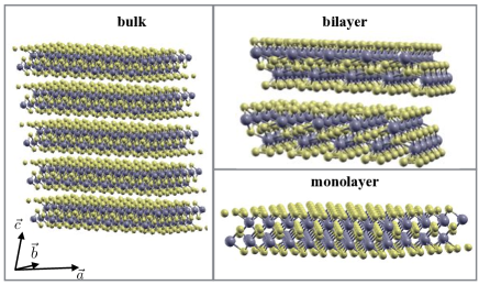
We have calculated the electronic band structure of mono- and bi-layer, and bulk TiS3. We show in Fig. 1 the atomic configurations of these materials. For the mono- and bi-layer material we found that they are direct gap semiconductors with a DFT gap of around 0.3 eV. On the other hand, the bulk material is predicted as an indirect gap semiconductor with a DFT gap of around 0.3 eV. In contrast, the experiments indicate that bulk TiS3 is a direct gap semiconductor with an electronic gap of about 1 eV 5, 7. For all the cases we have considered here, a more refined calculation based on non-self-consistent GW method (or hybrid functionals) opens up the gap to the experimental levels (about 1.0 eV), 8 but does not remove the discrepancy on the nature of the gap (these results are not shown here). From our work 7 with different pseudo-potentials it seems that a pivotal role in determining the nature of the gap in bulk TiS3 is played by the core electrons of the Ti atoms and in particular how they are described by the exchange-correlation potential used in the DFT calculation. We believe that this discrepancy between theory and experiment is still open and further investigation is necessary. On the other hand, we expect the nature of the gap does not play a crucial role on the way we control it via strain or pressure.
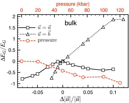
In order to study the strain induced band gap modulation, we applied a stress by deforming the length of the unit-cell vector in the or direction and relaxed the atomic positions.111We here neglect the effect of the Poisson’s deformation induced in the other two axes of the unit cell. Preliminary results have shown this effect to be negligible with Poisson’s ratios of the order of 0.04-0.08. These results will be presented elsewhere. In Fig. 2 one can see the indirect band gap change for bulk TiS3. refers to the band gap of the material when pressure or strain are not applied. While a negative strain (compression) in and direction of the unit cell leads to a reduction of the band gap, a positive strain can increase or decrease the band gap. A positive strain in the direction leads to an increase of the indirect band gap, while in the direction the positive strains induce a reduction of the electronic gap. In addition, we have studied the influence of an isotropic stress, hydrostatic pressure, on the bulk material. Pressure leads to a reduction of the band gap, which coincides with the results that negative stress in both and directions lead to a reduction of the gap. These findings are quite unique since for TDMs a tensile strain always reduces the band gap 19.
While for bulk we only find a reduction or increase of the gap, for monolayer and bilayer TiS3 we find additionally a direct-indirect transition, this might have important consequences to tailor the optical response of possible TiS3 based phototransistor. In Fig. 3 the influence of strain on the DFT gap of mono- and bi-layer TiS3 is shown. For both systems, while a compression in the direction reduces the direct gap, an expansion increases the gap until a strain of around and increasing the negative strain further leads to a reduction of the gap. Most interesting, a compression in direction leads to a reduction of the direct gap up to , applying or more strain transforms the gap to an indirect one by keeping the gap constant at around one third of its original value. As in the bulk material a positive strain in the direction leads to an monotonic increase of the gap.
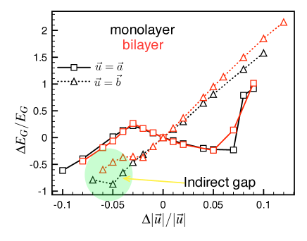
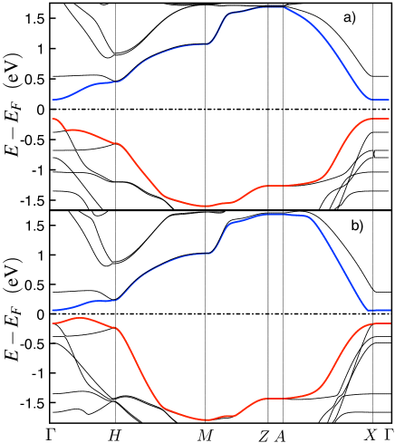
To better understand this transition, the band structure for the unstrained monolayer and 5% strain in the direction is shown in Fig. 4. We clearly see from Fig. 4 that the conduction bands is almost untouched by the compression, while the valence bands develops a local maximum between and , reducing the gap and changing its nature. Interestingly the reduction of the band-gap in the transition from direct to indirect is here more marked than what has been reported in TiS3 nano-ribbons, where the reported band gap modification is of only a few meV 20, in certain cases below the accuracy of the pseudo-potentials used in DFT.
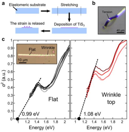
In order to experimentally verify the predicted effect of strain on the electronic band structure of TiS3 we study the optical absorption spectra of a thin TiS3 ribbon subjected to uniaxial strain. The strain is applied by exploiting the buckling-induced de-lamination process that takes place when a thin elastic film, deposited onto an elastomeric substrate, is subjected to a uniaxial compressive strain 21, 22. The trade-off between the bending rigidity of the thin-film and the thin-film/elastomeric substrate adhesion forms wrinkles that delaminate from the elastomeric substrate where the thin-film is uni-axially stretched. We address the reader to Ref. 23 for more details on the buckling-induced de-lamination process. Figure 5a shows a sketch of the process followed to fabricate the uni-axially strained TiS3 sample. A gelfilm substrate (a commercially available elastomeric substrate) is uni-axially stretched by 30, then TiS3 is deposited onto the stretched surface and the strain is suddenly released yielding to the buckling-induced de-lamination to the TiS3 (see Figure 5b) with flat regions (released stress) and delaminated wrinkles (accumulated tensile stress). For thin TiS3 ribbons (10 nm to 30 nm thick, like the one studied here) the wrinkles are 100 nm - 300 nm in height, the estimated maximum tensile strain on the topmost part is in the order of 0.3-0.7 21, 24. The change in the band structure induced by the applied uniaxial strain along is probed by a recently developed hyper-spectral imaging based absorption spectroscopy technique. We address the reader to Ref. 25 for details on this technique. Figure 5c shows the absorption spectra acquired on 9 flat regions and on top of 4 wrinkles. The intercept with the horizontal axis of the relationship vs. gives an estimate of the band gap (valid for direct gap semiconductors, for indirect ones it should be vs. ). The obtained band gap values in the flat region, 0.99 eV, is in good agreement with the value determined by conventional absorption spectroscopy and by photocatalysis measurements on bulk material 8, 26. On the topmost part of the wrinkles the slope of the absorption band edge increases considerably yielding an estimated band gap value of 1.08 eV, 90 meV higher than on the unstrained TiS3. This experimental observation proves that 0.3-0.7 % uniaxial tensile strain along locally changes the band structure opening the band gap, without changing the nature of the band-gap which remains direct (as evidenced by the marked linear behavior of the absorption band edge in the representation vs. ). The experimental value also confirms the quite high sensitivity of these samples as predicted by our calculations: From Fig. 2 one can infer for small amplitude strains the linear relation for strains in the direction in relatively good agreement with the experimental value 13-30. Note that the large uncertainty of the experimentally determined strain tunability stems from the difficulty in estimating the actual strain applied to the sample.
In conclusion, we have done a systematic investigation of the band gap modifications of monolayer, bilayer and bulk TiS3 material when the system is subject to strain or hydrostatic pressure. We found at zero applied strain or pressure an indirect gap for the bulk of around 0.28 eV, while for the mono- and bi-layer material we calculated a direct of 0.31 eV and 0.27 eV, respectively. These values, although in good agreement with other theoretical calculations, are about 1/3 of the experimental band gap value, a not surprising results considered that DFT usually underestimate the electronic band gap. We found that the gap can be controlled by inducing strain in certain directions along the primitive axes of the unit cell. Most interestingly, we found that the gap of the monolayer and bilayer material changes from direct to indirect when compressive strain is induced along the preferred transport axis ( in Fig. 1). We tested our predictions by inducing strain in a TiS3 sample: the gap increases when the system is under tensile strain, in agreement with the theoretical predictions of Fig. 2. This behavior is mostly noticeable, since for other two dimensional di-calchogenides materials the gap always closes for tensile strain, and can open a set of potential application for TiS3. Note added: During the elaboration of the manuscript the authors became aware of two theoretical works where, the general properties of the MX3 materials (where M = Ti, Zr and Hf; while X = S, Se, Te) 27, the effects of tensile a strain on the band gap of single layer 28 and nano-ribbons 22 of TiS3 are studied.
R.B. and R.D’A. acknowledge financial support by DYN-XC-TRANS (Grant No. FIS2013-43130-P), the Grupo Consolidado UPV/EHU del Gobierno Vasco (IT578-13), and NANOTherm (CSD2010-00044) of the Ministerio de Economia y Competitividad (MINECO). R. B. acknowledges the financial support of Ministerio de Educacion, Cultura y Deporte (FPU12/01576). R. D’A. is grateful to the Physics Department of King’s College London for its hospitality during the completion of this work supported by the Grant No. MV-2015-1-17 of the Diputacion Foral de Guipuzkoa. A.C.-G. acknowledges financial support from the BBVA Foundation through the fellowship “I Convocatoria de Ayudas Fundacion BBVA a Investigadores, Innovadores y Creadores Culturales” (“Semiconductores ultradelgados: hacia la optoelectronica flexible”). G. R.-B. acknowledges financial support from the Grant No. MAT2014-57915-R from the MINECO. The MIRE group acknowledge financial support from MINECO (MAT2011-22780) and E.F. thanks to the Mexican National Council for Science and Technology (CONACyT) for providing a PhD. Grant.
References
- Novoselov et al. 2004 Novoselov, K. S.; Geim, A. K.; Morozov, S. V.; Jiang, D.; Zhang, Y.; Dubonos, S. V.; Grigorieva, I. V.; Firsov, A. A. Science 2004, 306, 666
- Cahangirov et al. 2009 Cahangirov, S.; Topsakal, M.; Aktürk, E.; Sahin, H.; Ciraci, S. Phys. Rev. Lett. 2009, 102, 236804
- Yang et al. 2014 Yang, K.; Cahangirov, S.; Cantarero, A.; Rubio, A.; D’Agosta, R. Phys. Rev. B 2014, 89, 125403
- Cahangirov et al. 2013 Cahangirov, S.; Audiffred, M.; Tang, P.; Iacomino, A.; Duan, W.; Merino, G.; Rubio, A. Phys. Rev. B 2013, 88, 035432
- Endo et al. 1981 Endo, K.; Ihara, H.; Watanabe, K.; Gonda, S.-I. J. Solid State Chem. 1981, 39, 215–218
- Island et al. 2014 Island, J. O.; Buscema, M.; Barawi, M.; Clamagirand, J. M.; Ares, J. R.; Sánchez, C.; Ferrer, I. J.; Steele, G. a.; van der Zant, H. S. J.; Castellanos-Gomez, A. Adv. Opt. Mater. 2014, 2, 641
- Island et al. 2015 Island, J. O.; Barawi, M.; Biele, R.; Almazán, A.; Clamagirand, J. M.; Ares, J. R.; Sánchez, C.; van der Zant, H. S. J.; Álvarez, J. V.; D’Agosta, R.; Ferrer, I. J.; Castellanos-Gomez, A. Adv. Mater. 2015, 27, 2595
- Molina-Mendoza et al. 2015 Molina-Mendoza, A. J.; Barawi, M.; Biele, R.; Flores, E.; Ares, J. R.; Sánchez, C.; Rubio-Bollinger, G.; Agraït, N.; D’Agosta, R.; Ferrer, I. J.; Castellanos-Gomez, A. Adv. Electron. Mater. 2015, in press.
- Wu et al. 2015 Wu, J.; Wang, D.; Liu, H.; Lau, W.-M.; Liu, L.-M. RSC Adv. 2015, 5, 21455–21463
- Barawi et al. 2015 Barawi, M.; Ferrer, I. J.; Ares, J. R.; Sánchez, C. J. Mater. Chem. A 2015, 3, 7599
- Jin et al. 2015 Jin, Y.; Li, X.; Yang, J. Phys. Chem. Chem. Phys. 2015, 17, 18665–18669
- Gorlova et al. 2012 Gorlova, I.; Zybtsev, S.; Pokrovskii, V.; Bolotina, N.; Verin, I.; a.N. Titov, Phys. B Condens. Matter 2012, 407, 1707–1710
- Dai and Zeng 2015 Dai, J.; Zeng, X. C. Angew. Chemie Int. Ed. 2015, 54, 7572–7576
- Iyikanat et al. 2015 Iyikanat, F.; Sahin, H.; Senger, R. T.; Peeters, F. M. J. Phys. Chem. C 2015, 119, 10709–10715
- Giannozzi et al. 2009 Giannozzi, P. et al. J. Phys. Condens. Matter 2009, 21, 395502
- Hartwigsen et al. 1998 Hartwigsen, C.; Goedecker, S.; Hutter, J. Phys. Rev. B 1998, 58, 3641–3662
- Goedecker et al. 1996 Goedecker, S.; Teter, M.; Hutter, J. Phys. Rev. B 1996, 54, 1703–1710
- Furuseth et al. 1975 Furuseth, S.; Brattas, L.; Kjejshus, A. Acta Chem. Scand. 1975, 29, 623
- Roldán et al. 2015 Roldán, R.; Castellanos-Gomez, A.; Cappelluti, E.; Guinea, F. J. Phys. Condens. Matter 2015, 27, 313201
- Kang et al. 2015 Kang, J.; Sahin, H.; Ozaydin, H. D.; Senger, R. T.; Peeters, F. M. Phys. Rev. B 2015, 92, 075413
- Castellanos-Gomez et al. 2013 Castellanos-Gomez, A.; Roldán, R.; Cappelluti, E.; Buscema, M.; Guinea, F.; van der Zant, H. S. J.; Steele, G. A. Nano Lett. 2013, 13, 5361–5366
- Yang et al. 2015 Yang, S.; Wang, C.; Sahin, H.; Chen, H.; Li, Y.; Li, S.-S.; Suslu, A.; Peeters, F. M.; Liu, Q.; Li, J.; Tongay, S. Nano Lett. 2015, 15, 1660–1666
- Mei et al. 2011 Mei, H.; Landis, C. M.; Huang, R. Mech. Mater. 2011, 43, 627–642
- Vella et al. 2009 Vella, D.; Bico, J.; Boudaoud, A.; Roman, B.; Reis, P. M. Proc. Natl. Acad. Sci. 2009, 106, 10901–10906
- Castellanos-Gomez et al. 2015 Castellanos-Gomez, A.; Quereda, J.; van der Meulen, H.; Agraït, N.; Rubio-Bollinger, G. arXiv:1507.00869 2015,
- Ferrer et al. 2013 Ferrer, I.; Ares, J.; Clamagirand, J.; Barawi, M.; Sánchez, C. Thin Solid Films 2013, 535, 398–401
- Abdulsalam and Joubert 2015 Abdulsalam, M.; Joubert, D. P. Eur. Phys. J. B 2015, 88, 177
- Li et al. 2015 Li, M.; Dai, J.; Zeng, X. C. Nanoscale 2015, (accepted)