Current correlations in a Majorana beam splitter
Abstract
We study current correlations in a -junction composed of a grounded topological superconductor and of two normal-metal leads which are biased at a voltage . We show that the existence of an isolated Majorana zero mode in the junction dictates a universal behavior for the cross correlation of the currents through the two normal-metal leads of the junction. The cross correlation is negative and approaches zero at high bias voltages as . This behavior is robust in the presence of disorder and multiple transverse channels, and persists at finite temperatures. In contrast, an accidental low-energy Andreev bound state gives rise to nonuniversal behavior of the cross correlation. We employ numerical transport simulations to corroborate our conclusions.
pacs:
71.10.Pm, 74.45.+c, 74.78.Na, 73.50.TdI Introduction
Majorana bound states (MBS) in condensed matter physics are zero-energy modes which are bound to the boundaries of an otherwise gapped topological superconductor (TSC). Such an MBS is described by a self-adjoint operator and is protected against acquiring a finite energy. These properties are responsible for much of the great interest in MBSs Alicea (2012); Beenakker (2013).
Several theoretical proposals have been put forward for realizing topological superconductivity in condensed matter systems Moore and Read (1991); Fu and Kane (2008, 2009); Sau et al. (2010); Duckheim and Brouwer (2011); Oreg et al. (2010); Lutchyn et al. (2010); Nadj-Perge et al. (2013). Promising platforms include proximity-coupled semiconductor nanowires Lutchyn et al. (2010); Oreg et al. (2010) and ferromagnetic atomic chains Nadj-Perge et al. (2013); Braunecker and Simon (2013); Vazifeh and Franz (2013); Klinovaja et al. (2013); Pientka et al. (2013); Brydon et al. (2015); Peng et al. (2015); Dumitrescu et al. (2015), where recent transport measurements have provided compelling evidences for MBS formation Mourik et al. (2012); Deng et al. (2012); Das et al. (2012); Churchill et al. (2013); Finck et al. (2013); Nadj-Perge et al. (2014); Pawlak et al. ; Ruby et al. (2015).
Much emphasis has been put on investigating the differential conductance through a normal lead coupled to an MBS Bolech and Demler (2007); Law et al. (2009); Fidkowski et al. (2012); He et al. (2014). At low enough temperatures the differential conductance spectrum shows a peak at zero bias voltage which is quantized to . The observation of such conductance quantization has proved to be difficult, because it requires the temperature to be much lower than the width of the peak.
Alternatively, one can seek for signatures of an MBS in current correlations. Various aspects of current noise in topological superconducting systems have been studied Bolech and Demler (2007); Nilsson et al. (2008); Golub and Horovitz (2011); Wu and Cao (2012); Liu et al. (2013, 2015). Here, we consider a setup composed of multiple leads coupled to an MBS, which we term a “Majorana beam splitter” (Fig. 1), and study the cross correlations of the currents in the leads. In a recent work Haim et al. (2015) we have examined the cross correlation between currents of opposite spin emitted from an MBS, showing that it is negative in sign and approaches zero at high bias voltage. In the present work we show that this result holds much more generally: The cross correlation of any two channels in the beam splitter has the same universal characteristics, i.e., it is negative and approaches zero at voltages larger than the width of the Majorana resonance, independently of whether the different channels are spin resolved or not. An immediate experimental consequence is that this effect can be observed in a much less challenging setup, which does not require spin filters to resolve the current into its spin components.
The rest of this paper is organized as follows. In Sec. II we describe the setup under study and state our main results. In Sec. III we employ a simple model for the Majorana beam splitter, and calculate the current cross correlation using a scattering-matrix approach. In Sec. IV we corroborate our conclusions in a numerical simulation of a microscopic model, comprising a proximity-coupled semiconductor wire. In Sec. V we present a semiclassical picture of transport, and use it to rederive our results in the high-voltage limit. This is done in a way which relates the result of this paper to the nonlocal nature of MBSs. Finally, we conclude in Sec. VI.
II Setup and main result
 |
(a)
 (b)
(b)
|
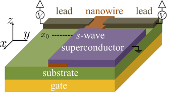
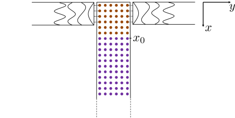
We consider a -junction between a topological superconductor (TSC) and two normal-metal leads as depicted in Fig. 1(a). We study the low-frequency cross correlation of the currents through the two arms of the junction, namely
| (1) |
where , and are the current operators in the right and left arm of the junction respectively Psy . The brackets stand for thermal quantum averaging. We denote the width of the resonance due to the MBS by , and the excitation gap by Exc . A voltage is applied between the superconductor and the leads. Below we show that in the regime , has a simple, universal behavior, given by Eq. (9). In particular, is negative, and approaches zero when . For the behavior is nonuniversal.
This effect survives, to a large extent, at finite temperatures. As long as the temperature is smaller than , is only weakly temperature dependent, even if . This is in contrast to the zero-bias peak in the differential conductance spectrum which is only quantized to for .
Unlike studies which have focused on the cross correlation between currents through two MBSs at the two ends of a TSC Nilsson et al. (2008); Bose and Sodano (2011); Lü et al. (2012); Liu et al. (2013); Zocher and Rosenow (2013), here the effect is due to a single MBS. In Ref. [Nilsson et al., 2008; Bose and Sodano, 2011; Lü et al., 2012; Liu et al., 2013; Zocher and Rosenow, 2013] it was crucial that the MBSs at the two ends of the TSC were coupled Maj . Here, on the other hand, the effect is most pronounced when the two MBSs are spatially separated such that only a single MBS is coupled to the leads.
III Scattering matrix approach
The proposed experimental setup is described in Fig. 1(a). A semiconductor nanowire is proximitized to a grounded -wave superconductor. When a sufficiently strong magnetic field is applied, the wire enters a topological phase Lutchyn et al. (2010); Oreg et al. (2010), giving rise to an MBS at each end. One of the wire’s ends is coupled to two metallic leads, both biased at a voltage .
To calculate the currents through the leads and their cross correlation we use the Landauer-Büttiker formalism in which transport properties are obtained from the scattering matrix, describing both normal and Andreev scattering. We are interested in bias voltages smaller than the gap, Exc . An electron incident from one of the normal leads is therefore necessarily reflected from the middle (superconducting) leg. It can be reflected to the right or the left lead, either as an electron or as a hole. Since there is no transmission into the superconductor, scattering is described solely by a reflection matrix.
Each normal lead contains transverse channels, including both spin species. The overall reflection matrix which we wish to obtain reads
| (2) |
where each block is a matrix. The matrix element , where , is the amplitude for a particle of type coming from the channel to be reflected into the channel as a particle of type . Here, enumerates the channels in the right lead while enumerates the channels in the left lead.
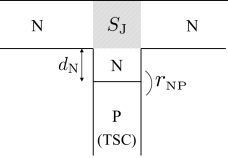
We model the TSC as a spinless -wave superconductor which is a valid description close to the Fermi energy Alicea et al. (2011); Rieder et al. (2012). It is convenient to insert a (spinless) normal-metal section between the TSC and the junction. In this way, we separate the scattering in the -junction itself from the scattering at the normal–-wave interface (cf. Fig. 1b). The length of the normal-metal section is then taken to zero.
Andreev reflection at the normal–-wave superconductor interface is described by
| (3) |
where is the Andreev reflection amplitude for Andreev (1964); Beenakker (1991), with being the energy as measured from the Fermi level. The information about the topological nature of the system is encoded in . The relative minus sign between the off-diagonal elements of signals that the pairing potential of the superconductor has a -wave symmetry. Moreover, the nontrivial topological invariant Merz and Chalker (2002); Akhmerov et al. (2011) dictates the existence of an MBS at each end of the superconductor.
Scattering at the -junction (which connects the added normal section to the two leads) is described by
| (4) |
where describes scattering of electrons and describes scattering of holes. Here, is a matrix describing the reflection of electrons coming from the left and right leads (each having transverse channels), is a reflection amplitude for electrons coming from the middle leg (having a single channel), is a transmission matrix of electrons from the right and left leads into the middle leg, and is a transmission matrix of electrons from the middle leg into the right and left leads. The matrix is assumed to be energy-independent in the relevant energy range, but is otherwise a completely general unitary matrix.
We can now concatenate with to obtain the overall reflection matrix of Eq. (2). The block is obtained by summing the contributions from all the various trajectories in which an electron is reflected back as an electron, while the block is obtained by summing those trajectories in which an electron is reflected as a hole. This yields
| (5a) | ||||
| (5b) | ||||
The two other blocks are given by and in compliance with particle-hole symmetry Beenakker (2015).
Given the blocks of the reflection matrix, the sum of currents in the leads and their cross correlation are obtained by Anantram and Datta (1996)
| (6) |
where is the total current in the leads, and with being the distribution of incoming electrons in the leads. Here, the index runs only over the channels of the right lead, while the index runs only over those of the left lead. We use a convention in which for and for . At zero temperature Eq. (6) reduces to Nilsson et al. (2008)
| (7) |
where .
Let us introduce the parameter representing total normal transmission from the two leads into the middle leg of the -junction. Inserting Eq. (5) into Eq. (7) and using the unitarity of , we first obtain the differential conductance
| (8) |
where . As expected has a peak at which is quantized to . Similarly, we obtain for the cross correlation dif
| (9) |
where (note that ). The cross correlation is negative for all and approaches zero as for . This result is valid for . It is valid even in the presence of strong disorder in the junction region, as we did not assume a particular form of . Moreover, it does not depend on a specific realization of the TSC hosting the MBS.
The low-voltage behavior of the result in Eq. (9) can be understood from simple considerations based on the properties of MBSs. For and at zero temperature the conductance through the MBS is quantized to , resulting in an overall noiseless current Noi . Upon splitting the current into the two parts and , the total noise is related to the cross correlation via , where and are the current noises through the right and left leads, respectively Psy . Since at low voltage, while and are non-negative by definition, one must have . More specifically, at zero voltage the total noise obeys Golub and Horovitz (2011) . In addition, since (for zero temperature) , one has . It therefore follows that . The cross correlation is thus negative at low voltage.
IV Numerical Analysis
We now turn to illustrate the results of the previous section using numerical simulations. We consider the system depicted in Fig. 1(a). A semiconductor nanowire of dimensions is proximity coupled to a conventional -wave superconductor and is placed in an external magnetic field.
The Bogoliubov de-Gennes Hamiltonian describing the nanowire is given in Nambu representation, , by
| (10) |
where is the effective mass of the electron, includes both the chemical potential and a disordered potential, is the Rashba spin-orbit coupling strength, is the magnetic field directed along the wire, is the Bohr magneton, is the Landé -factor, is the proximity-induced pair potential, and and are vectors of Pauli matrices in spin and particle-hole space, respectively. Since we take to be much smaller than the magnetic length, we can ignore the orbital effect of the magnetic field.
We approximate the continuum model of Eq. (10) by a tight-binding Hamiltonian
| (11) |
where runs over the sites of an by square lattice with spacing . Here , , , is the chemical potential, and is a Gaussian-distributed disorder potential with zero average and correlations .
We express in a first quantized form as a matrix , from which one extracts the retarded Green function
| (12) |
and subsequently the reflection matrix Fisher and Lee (1981); Iida et al. (1990)
| (13) |
Here, is a matrix describing the coupling of the eigenmodes in the leads to the end of the nanowire as depicted in Fig. 1(a) and specified in Appendix B. The metallic leads are described in the wide band limit by an energy independent . With the help of Eqs. (2) and (6) we then obtain the currents through the leads and their cross correlation
 (a)
(a)
 (b)
(b)
|
In the present work we use parameters consistent with an InAs nanowire, namely , , and Das et al. (2012). The induced pair potential is taken to be . The length of the wire is , with the section not covered by the superconductor being in length, and the width of the wire is .
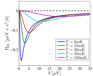
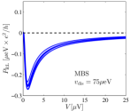
In Fig. 2 we present the cross correlation and the differential conductance at various temperatures for and . For these values of and the system is in the topological phase Oreg et al. (2010); Lutchyn et al. (2010, 2011). is negative and approaches zero at high voltages, in agreement with the analytic expression of Eq. (9). Interestingly, this behavior persists even at nonzero temperatures. The main effect of temperature is to increase the voltage above which starts approaching zero. Since the gap in the system is about , the effect can be seen even at the relatively high temperature of , a temperature for which the zero-bias conductance peak is much lower than .
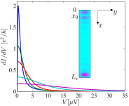
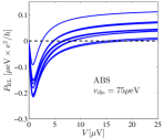
Next, we study the effect of disorder on . Figure 3(a) presents for 10 different realizations of random disorder with . As expected, the behavior of does not change significantly. We can compare this to the case of an ordinary Andreev state which is tuned to zero energy. The end of the wire which is not covered by a superconductor ( in Fig. 1(a)) hosts Andreev bound states which are coupled to the leads. For each realization of disorder, we tune the magnetic field to bring one of them to zero energy dWa , and calculate . In all the realizations, the resulting tuned magnetic field was below the critical field , i.e., the system is in the trivial phase. As shown in Fig. 3(b), the behavior of is nonuniversal and varies significantly from one realization of disorder to another. Importantly, in all cases is positive at large .
 (a)
(a)
|
 (b)
(b)
|
In our simulations we have chosen the length of the wire to be sufficiently bigger than the localization length of the Majorana wave function (which here is about ), so that the leads are only coupled to a single MBS. If becomes of the order of , say by increasing the magnetic field , then the leads become coupled also to the MBS at the other end of the wire. At this point it is as if the leads are coupled to a single ABS. Increasing the magnetic field therefore induces a crossover between the MBS case and the ABS case, in exactly the same way which was described and analyzed in Ref. [Haim et al., 2015].
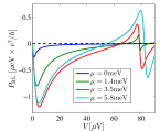
It is interesting to examine the case when more than a single transverse channel is occupied in the wire. For weak pairing Wea , the system is in the topological phase whenever an odd number of channels is occupied. Figure 4 presents and for various values of , each corresponding to a different odd number of occupied channels between and . When more than a single channel is occupied we can have subgap Andreev bound states which coexist with the MBS. One such state can be seen in Fig. 4(b) as a peak at . It is only below this voltage that the behavior of remains qualitatively the same as in the single channel case. In this respect, the existence of subgap states reduces the effective energy gap below which exhibits its universal features. Another effect of introducing higher transverse channels is the stronger coupling of the middle leg of the -junction to the two leads inc .
 (a)
(a)
|
 (b)
(b)
|
V Semiclassical Picture
The behavior of the current cross-correlation, as given in Eq. (9), at high voltages can be derived based on simple semiclassical considerations. We reconsider the setup shown in Fig. 1(a), and examine the limit , where is the width of the zero-energy resonance (which can be either an MBS or an ABS).
In this limit, the transport of current from the superconductor to the leads can be described in terms of a sequence of tunneling events. In each tunneling event, a Cooper pair in the superconductor dissociates; one electron is emitted into the right or left lead, and the other is absorbed into the zero mode localized at the edge of the superconductor. In the presence of such a zero mode, the many–body ground state of the superconductor is doubly degenerate. We denote the two ground states by and , corresponding to an even and odd number of electrons in the superconducting wire, respectively. Each time an electron is emitted into the leads, the superconductor flips its state from to or vice versa.
Let us denote by and the probability per unit time to emit an electron into the right or left lead, respectively, given that the superconductor is in state . Similarly, are the corresponding rates when the system is in the state.
After a time , there are and electrons emitted to the right and left leads respectively. The average currents in the leads are given by
| (14) |
and the current cross correlation is given by
| (15) |
In the case of a Majorana zero mode, all the local properties of the states and are identical. This is usually stated as the fact that one cannot make a local measurement which would reveal in which of the two ground states the system is in. In particular, this implies that and . Let us divide the time into short time intervals ; is the minimal time between consecutive emission events (set by the minimal temporal width of an electron wave packet whose energy spread is ). At each time step , either an electron is emitted to the right lead, an electron is emitted to the left lead, or no electron is emitted at all. The transport process is thus described by a trinomial distribution. The probabilities of being emitted to the right and left lead are and , respectively, and there are overall time steps. One thus obtains Papoulis (1984)
| (16) | ||||
Finally, inserting Eq. (16) into Eqs. (14) and (15) one has
| (17) |
and
| (18) |
is negative and approaches zero as . We have therefore reproduced the high-voltage limit of Eq. (9).
Unlike the case of an MBS, for an ABS the probabilities to emit an electron to the right or the left lead can depend on the state of the system, or . To illustrate the effect this dependence has on the cross correlations, we consider the case
| (19) |
where the electron can only go right if the system is in , and it can only go left if the system is in Foo . Because each time an electron is transmitted the state of the system changes (either from to or vice versa), it is clear that . For simplicity we assume . In this case, the distribution for the total number of emitted electrons is binomial; in each time step we only ask whether an electron has been emitted to one of the leads or not. The probability for an electron to be emitted is . Remembering that half of the times the electron is emitted to the right and half of the times to the left, one obtains
| (20) |
Inserting this into Eq. (15) one has
| (21) |
where is a constant of order unity. is monotonically increasing, asymptotically approaching a positive constat. This is in agreement with Fig. 3(b) and with the results of Ref. [Haim et al., 2015].
VI Conclusions
When current from a topological superconductor is split into two metallic leads, the current cross correlation exhibits universal behavior as a function of bias voltage . The cross correlation is negative for all and approaches zero at high voltage as . This behavior is robust and does not rely on a specific realization of the topological superconductor hosting the Majorana, or on a specific form of coupling to the leads. It can be observed even in disordered multichannel systems at finite temperature. For the effect to be observed the width of the Majorana resonance has to be smaller than the energy of the first subgap state. Importantly, the temperature does not have to be smaller than .
In contrast, for the case of an accidental low-energy ABS, is nonuniversal. In particular, it is sensitive to details such as the realization of disorder.
The result of this work for the current cross correlation has its roots in the defining properties of MBSs. The high-voltage behavior can be shown to stem from the nonlocal nature of MBS; the fact that the occupation of the Majorana mode cannot be revealed by any local probe. The low-voltage behavior stems from the fact that the MBS induces perfect Andreev reflection at zero bias.
ACKNOWLEDGEMENTS
We acknowledge discussions with C. W. J. Beenakker and A. M. Finkelstein. This study was supported by the Israel Science Foundation (ISF), Minerva grants, a Career Integration Grant (CIG), a Minerva ARCHES prize, the Helmholtz Virtual Institute “New States of Matter and their Excitations”, and an ERC grant (FP7/2007-2013) 340210.
Note added in proof.— We became aware of two recent papers by Valentini et al. Valentini et al. (2016) and by Tripathi et al. Tripathi et al. . Our results are consistent with theirs where they overlap.
Appendix A Hamiltonian Approach
The results presented in Eqs. (8) and (9) of Sec. III can be derived from a Hamiltonian approach of transport. We start from an effective low-energy Hamiltonian describing a multiple number of conducting channels which are coupled to a single MBS. Each of the channels belongs either to the left lead or to the right lead (although the calculation proceeds similarly in the case of a different number of leads). The Hamiltonian reads
| (22) |
where describes the MBS, creates an electron with momentum and energy in the channel, and is the coupling constant of the channel to the Majorana.
In the wide-band limit the reflection matrix can be obtained by Fisher and Lee (1981); Iida et al. (1990)
| (23) |
with being a vector of coupling constants given by
| (24) |
where is the density of states of the channel at the Fermi energy, and is the number of spinful channels in each lead (all together there are electronic channels). One obtains for the blocks of [see also Eq. (2)]
| (25) |
with and , and where we have defined .
Inserting Eq. (25) into Eq. (7) results in
| (26) |
and
| (27) |
where . We have therefore rederive Eqs. (8) and (9). We note that the definition of here is in terms of the coupling constant, while in Sec. III it is given in terms of transmission amplitudes. In both cases, however, it equals the width of the Majorana-induced resonance.
Appendix B Details of Numerical Simulations
To obtain the scattering matrix using Eqs. (11-13) we express the Hamiltonian in first quantized form using a matrix defined by
| (28) |
where creates an electron with spin on site of an square lattice. Here, for spin and for spin . In our simulations we used , and .
The matrix in Eq. (12) describes the coupling between the extended modes of the leads and the sites of the lattice. In each lead there are spinful transverse channels. In our simulations (see Fig. 5). Including both leads, both spin species, and the particle-hole degree of freedom, is a matrix of the following form
| (29) |
where and described the coupling to the left and right lead, respectively. As depicted in Fig. 5, each lead is coupled only to those lattice sites which are adjacent to it. Moreover, the coupling to each site is modulated according to the transverse profile of the particular channel. This is described by
| (30) |
where is a identity matrix in spin space, and is a set of coupling constants for each transverse channel of the leads. In this work we have used .
Given the coupling matrix and the first-quantized Hamiltonian , the reflection matrix is calculated using Eqs. (12) and (13).
References
- Alicea (2012) J. Alicea, Rep. Prog. Phys. 75, 076501 (2012).
- Beenakker (2013) C. W. J. Beenakker, Ann. Rev. Condens. Matt. Phys. 4, 113 (2013).
- Moore and Read (1991) G. Moore and N. Read, Nucl. Phys. B 360, 362 (1991).
- Fu and Kane (2008) L. Fu and C. L. Kane, Phys. Rev. Lett. 100, 096407 (2008).
- Fu and Kane (2009) L. Fu and C. L. Kane, Phys. Rev. B 79, 161408 (2009).
- Sau et al. (2010) J. D. Sau, R. M. Lutchyn, S. Tewari, and S. Das Sarma, Phys. Rev. Lett. 104, 040502 (2010).
- Duckheim and Brouwer (2011) M. Duckheim and P. W. Brouwer, Phys. Rev. B 83, 054513 (2011).
- Oreg et al. (2010) Y. Oreg, G. Refael, and F. von Oppen, Phys. Rev. Lett. 105, 177002 (2010).
- Lutchyn et al. (2010) R. M. Lutchyn, J. D. Sau, and S. Das Sarma, Phys. Rev. Lett. 105, 077001 (2010).
- Nadj-Perge et al. (2013) S. Nadj-Perge, I. K. Drozdov, B. A. Bernevig, and A. Yazdani, Phys. Rev. B 88, 020407 (2013).
- Braunecker and Simon (2013) B. Braunecker and P. Simon, Phys. Rev. Lett. 111, 147202 (2013).
- Vazifeh and Franz (2013) M. M. Vazifeh and M. Franz, Phys. Rev. Lett. 111, 206802 (2013).
- Klinovaja et al. (2013) J. Klinovaja, P. Stano, A. Yazdani, and D. Loss, Phys. Rev. Lett. 111, 186805 (2013).
- Pientka et al. (2013) F. Pientka, L. I. Glazman, and F. von Oppen, Phys. Rev. B 88, 155420 (2013).
- Brydon et al. (2015) P. M. R. Brydon, S. Das Sarma, H.-Y. Hui, and J. D. Sau, Phys. Rev. B 91, 064505 (2015).
- Peng et al. (2015) Y. Peng, F. Pientka, L. I. Glazman, and F. von Oppen, Phys. Rev. Lett. 114, 106801 (2015).
- Dumitrescu et al. (2015) E. Dumitrescu, B. Roberts, S. Tewari, J. D. Sau, and S. Das Sarma, Phys. Rev. B 91, 094505 (2015).
- Mourik et al. (2012) V. Mourik, K. Zuo, S. Frolov, S. Plissard, E. Bakkers, and L. Kouwenhoven, Science 336, 1003 (2012).
- Deng et al. (2012) M. T. Deng, C. L. Yu, G. Y. Huang, M. Larsson, P. Caroff, and H. Q. Xu, Nano Lett. 12, 6414 (2012).
- Das et al. (2012) A. Das, Y. Ronen, Y. Most, Y. Oreg, M. Heiblum, and H. Shtrikman, Nat. Phys. 8, 887 (2012).
- Churchill et al. (2013) H. O. H. Churchill, V. Fatemi, K. Grove-Rasmussen, M. T. Deng, P. Caroff, H. Q. Xu, and C. M. Marcus, Phys. Rev. B 87, 241401 (2013).
- Finck et al. (2013) A. D. K. Finck, D. J. Van Harlingen, P. K. Mohseni, K. Jung, and X. Li, Phys. Rev. Lett. 110, 126406 (2013).
- Nadj-Perge et al. (2014) S. Nadj-Perge, I. K. Drozdov, J. Li, H. Chen, S. Jeon, J. Seo, A. H. MacDonald, B. A. Bernevig, and A. Yazdani, Science 346, 602 (2014).
- (24) R. Pawlak, M. Kisiel, J. Klinovaja, T. Meier, S. Kawai, T. Glatzel, D. Loss, and E. Meyer, arXiv:1505.06078 .
- Ruby et al. (2015) M. Ruby, F. Pientka, Y. Peng, F. von Oppen, B. W. Heinrich, and K. J. Franke, Phys. Rev. Lett. 115, 197204 (2015).
- Bolech and Demler (2007) C. J. Bolech and E. Demler, Phys. Rev. Lett. 98, 237002 (2007).
- Law et al. (2009) K. T. Law, P. A. Lee, and T. K. Ng, Phys. Rev. Lett. 103, 237001 (2009).
- Fidkowski et al. (2012) L. Fidkowski, J. Alicea, N. H. Lindner, R. M. Lutchyn, and M. P. A. Fisher, Phys. Rev. B 85, 245121 (2012).
- He et al. (2014) J. J. He, T. K. Ng, P. A. Lee, and K. T. Law, Phys. Rev. Lett. 112, 037001 (2014).
- Nilsson et al. (2008) J. Nilsson, A. R. Akhmerov, and C. W. J. Beenakker, Phys. Rev. Lett. 101, 120403 (2008).
- Golub and Horovitz (2011) A. Golub and B. Horovitz, Phys. Rev. B 83, 153415 (2011).
- Wu and Cao (2012) B. H. Wu and J. C. Cao, Phys. Rev. B 85, 085415 (2012).
- Liu et al. (2013) J. Liu, F.-C. Zhang, and K. T. Law, Phys. Rev. B 88, 064509 (2013).
- Liu et al. (2015) D. E. Liu, M. Cheng, and R. M. Lutchyn, Phys. Rev. B 91, 081405 (2015).
- Haim et al. (2015) A. Haim, E. Berg, F. von Oppen, and Y. Oreg, Phys. Rev. Lett. 114, 166406 (2015).
- (36) We note that the zero-frequency correlation matrix is symmetric, namely . A proof can be found in Appendix B of Anantram et al. Anantram and Datta (1996).
- (37) The excitation gap is either the superconducting gap, or the energy gap to the next subgap state (if such are present) above the Majorana zero-energy bound state.
- Bose and Sodano (2011) S. Bose and P. Sodano, New J. Phys. 13, 085002 (2011).
- Lü et al. (2012) H.-F. Lü, H.-Z. Lu, and S.-Q. Shen, Phys. Rev. B 86, 075318 (2012).
- Zocher and Rosenow (2013) B. Zocher and B. Rosenow, Phys. Rev. Lett. 111, 036802 (2013).
- (41) The coupling between the Majorana bound states is established either through a tunneling term, or through a nonlocal charging-energy term.
- Alicea et al. (2011) J. Alicea, Y. Oreg, G. Refael, F. von Oppen, and M. P. Fisher, Nat. Phys. 7, 412 (2011).
- Rieder et al. (2012) M.-T. Rieder, G. Kells, M. Duckheim, D. Meidan, and P. W. Brouwer, Phys. Rev. B 86, 125423 (2012).
- Andreev (1964) A. Andreev, Zh. Eksp. Teor. Fiz. 46, 1823 (1964).
- Beenakker (1991) C. W. J. Beenakker, Phys. Rev. Lett. 67, 3836 (1991).
- Merz and Chalker (2002) F. Merz and J. T. Chalker, Phys. Rev. B 65, 054425 (2002).
- Akhmerov et al. (2011) A. R. Akhmerov, J. P. Dahlhaus, F. Hassler, M. Wimmer, and C. W. J. Beenakker, Phys. Rev. Lett. 106, 057001 (2011).
- Beenakker (2015) C. W. J. Beenakker, Rev. Mod. Phys. 87, 1037 (2015).
- Anantram and Datta (1996) M. P. Anantram and S. Datta, Phys. Rev. B 53, 16390 (1996).
- (50) For an alternative derivation of this result using a Hamiltonian formalism see Appendix A.
- (51) More specifically, the reflection matrix contains one channel which perfectly Andreev reflects, while the rest of the channels have perfect normal reflection in the weak coupling limit, .
- Fisher and Lee (1981) D. S. Fisher and P. A. Lee, Phys. Rev. B 23, 6851 (1981).
- Iida et al. (1990) S. Iida, H. A. Weidenmüller, and J. Zuk, Ann. Phys. 200, 219 (1990).
- (54) Notice that at zero temperature and at zero bias voltage the differential conductance drops to zero. This is due to a finite-size effect, coming from the exponentially small energy splitting, , between the two Majorana end states. For weak overlap of the Majoranas, the conductance approaches at a voltage .
- Lutchyn et al. (2011) R. M. Lutchyn, T. D. Stanescu, and S. Das Sarma, Phys. Rev. Lett. 106, 127001 (2011).
- (56) Low-energy ABSs can also occur naturally in various systems, for example, at the edge of a -wave superconductor, see Y. Tanaka and S. Kashiwaya, Phys. Rev. Lett. 74, 3451 (1995).
- (57) Weak pairing here means that the pairing potential is smaller than the Zeeman splitting and the energy spacing between transverse channels.
- (58) This can be seen from the fact that the width of the zero-bias resonance in Fig. 4(b) becomes larger for higher numbers of transverse channels.
- Papoulis (1984) A. Papoulis, Probability, Random Variables, and Stochastic Processes (2nd ed. New York: McGraw-Hill, 1984).
- (60) This resembles the case studied in Ref. [Haim et al., 2015] of spin-resolved transport through an ABS in a system which conserves the -component of the spin. There, the emitted electron can only have spin up (down) if the superconductor is in the state (), respectively.
- Valentini et al. (2016) S. Valentini, M. Governale, R. Fazio, and F. Taddei, Physica E 75, 15 (2016).
- (62) K. M. Tripathi, S. Das, and S. Rao, arXiv:1509.06684 .