Silicon and silicon-nitrogen impurities in graphene: structure, energetics and effects on electronic transport
Abstract
We theoretically study the atomic structure and energetics of silicon and silicon-nitrogen impurities in graphene. Using density-functional theory, we get insight into the atomic structures of the impurities, evaluate their formation energies and assess their abundance in realistic samples. We find that nitrogen, as well as oxygen and hydrogen, are trapped at silicon impurities, considerably altering the electronic properties of the system. Furthermore, we show that nitrogen doping can induce local magnetic moments resulting in spin-dependent transport properties,even though neither silicon nor nitrogen impurities are magnetic by themselves. To simulate large systems with many randomly distributed impurities, we derive tight-binding models that describe the effects of the impurities on graphene electron structure. Then by using the linear-scaling real-space Kubo-Greenwood method, we evaluate the transport properties of large-scale systems with random distribution of impurities, and find the fingerprint-like scattering cross sections for each impurity type. The transport properties vary widely, and our results indicate that some of the impurities can even induce strong localization in realistic graphene samples.
pacs:
61.48.Gh, 61.72.-yI Introduction
Graphene is a remarkable two-dimensional (2D) material due to its unique mechanical and electronic properties, which makes it a good candidate for modern nanoscale devices and applications. While pristine graphene is a semimetal with a high carrier mobility Novoselov et al. (2005); Chen et al. (2008); Morozov et al. (2008); Siegel et al. (2011); Castro Neto et al. (2009), for some applications it would be desirable to open a band gap in it, for example by cutting it to ribbons Son et al. (2006a); Yang et al. (2007); Han et al. (2007) or introducing impurities and defectsBerashevich and Chakraborty (2009); Balog et al. (2010); Casolo et al. (2011); Denis (2010). Moreover, impurities are often the dominant scatterers that control the intrinsic electronic and transport properties of realistic systems.
Silicon is commonly present in nature, so that Si impurities can appear in synthetic graphene during the growth processes or be introduced later when graphene is used together with standard silicon-based electronics components. It is even preferred to grow graphene on silicon wafers as one does not have to transfer it elsewhere after growth. Specifically, graphene grown at high temperatures by chemical vapor deposition can introduce silicon and oxygen impurities originating from the quartz (SiO2) substrate or the apparatus itself. Also using silicon carbide (SiC) Forbeaux et al. (1998); Singh et al. (2011) to grow graphene can produce silicon impurites. Another avenue would be to deliberately introduce silicon impurities by post-synthesis treatments Wang et al. (2012, 2014), such as by low-energy ion irradiation, similar to direct ion implantation of N and B atoms into single graphene sheets Bangert et al. (2013), or deposition of Si atoms on ion or electron-beam treated graphene with irradiation-induced vacancies. Silicon atoms filling monovacancies and divacancies in graphene have been explicitly identified in experiments Zhou et al. (2012a); Ramasse et al. (2013). Their formation energies are expected to be fairly low compared to other period 3 element substitution defects Denis (2010), and they are stable enough for the electron beam not to break the atomic structure or the bonding easily Zhou et al. (2012b).
Si impurities can further pick-up various atoms from the environment. Recent experimental studies have reported the presence of individual defects formed by co-occurring silicon and nitrogen impurities Zhou et al. (2012a, b). Zhou et al. showed that surface plasmons are locally enhanced at both silicon and a silicon-nitrogen impurities Zhou et al. (2012b). Therefore, such silicon impurities occurring in graphene could in principle be used as plasmonic waveguides. Additionally, they could be useful in optoelectronic devices Bonaccorso et al. (2010). Nitrogen impurities have been extensively studied, as they dope their surroundings in graphene Wei et al. (2009); Lambin et al. (2012), but the role of nitrogen binding to the silicon impurities, forming silicon-nitrogen defects, is not fully understood. Moreover, the presence of oxygen can also affect the formation of silicon impurities. We answer these issues by finding the defect geometries and formation energies for various silicon, silicon-oxygen and silicon-nitrogen impurities through comprehensive density-functional-theory calculations in a supercell geometry.
Such impurities are also interesting in the context of magnetism. Local magnetic moments can be created in graphene in several ways. Examples include graphene nanoribbon zigzag edges Son et al. (2006b), monovacancies and hydrogen adatoms Yazyev and Helm (2007), and transition metal substitutions Krasheninnikov et al. (2009). Local magnetic impurities interact strongly with the conduction electrons of graphene, as has been shown by measuring the Kondo effect Chen et al. (2011). We demonstrate that many of the nitrogen-doped silicon impurities exhibit finite spin moments. Such defects can be important in graphene-based spintronics applications, and we evaluate the spin-dependent electronic and transport properties for the most stable defect types.
Electronic transport in systems with silicon point-defects has been studied in a ribbon geometry by Lopez-Bezanilla et al. Lopez-Bezanilla et al. (2014). They found that the formation energies of the silicon point-defects are smaller closer to the ribbon edges, and the transmission functions for graphene nanoribbons with silicon defects at the edges were computed. Furthermore, Cheng et al. Cheng et al. (2014) studied the electronic and transport properties of the SiNx defects in armchair nanoribbons. However, it is unclear what are the transport properties of realistic two-dimensional graphene systems with numerous randomly positioned defects. We simulate transport in such a realistic setting, and find the characteristic fingerprint-like scattering cross sections for each defect type.
The paper is organized as follows. In Sections II A-D, we present first principles results for the geometries and formation energies of silicon, silicon-oxygen, and silicon-nitrogen impurities, and also touch upon the effects of hydrogen adsorption on them. In section II E, we evaluate the electronic band structures and density of states of systems containing silicon and silicon-nitrogen impurities. In Section III A-B we derive tight-binding models to describe the effects of the impurities on the electronic structure. In Section III C, we compare the density of states of the system with impurities calculated within the periodic supercell approach with that of many randomly placed impurities in large realistic systems. In Section III D, we report the results of a comprehensive real-space Kubo-Greenwood study of the electronic transport of silicon and silicon-nitrogen impurities, where we also discuss the localization effects in these systems.
II First principles calculations
First principles calculations were performed by the all-electron density-functional theory package FHI-aims Blum et al. (2009). The code uses local basis functions specified for each atom, and we have chosen the default tight basis sets provided in the package. As the exchange-correlation energy functional we used the generalized-gradient approximation as parametrized by Perdew, Burke, and Ernzerhof (PBE) Perdew et al. (1996).
The defects were placed in periodic supercells of and graphene unit cells. Without any defects they would contain and carbon atoms, respectively. The lattice vectors of the supercells were fixed to those of pristine graphene (with a lattice constant of Å in a two-atom unit cell), even after the point-defects had been introduced. The atom positions were relaxed until the forces between the atoms were smaller than eV/Å. The self-consistency cycle was considered converged if the change in the volume-integrated root-mean square of the charge density, and changes in the sum of eigenvalues and total energy were below [electrons], eV, and eV, respectively. A Monkhorst-Pack grid of k-points was employed in the total energy calculations, and the band structure and density of states (DOS) calculations utilized a -centered grid with at least k-points in order to achieve a better coverage of the first Brillouin zone.
Performing the calculations with two distinct supercell sizes lets us explicitly test whether the results have converged as a function of system size. Systematic convergence studies have been done for the silicon substitution defect in graphene in Ref. [Denis, 2010], where convergent results were obtained already with a rather small supercell, as contrary to vacanciesKrasheninnikov and Nieminen (2011), substitutional impurities and adatoms do not give rise to long-ranged strain fields. Studying structural point-defects in graphene, a supercell is typically large enough for geometry relaxation Lherbier et al. (2012). However, to obtain convergent electronic properties and spectra, a larger supercell is typically needed. Specifically, for isolated nitrogen substitution defect, or any other defect with large effective on-site potential at the impurity site, the supercell needs to be much largerLambin et al. (2012). The same is true for the adequate description of magnetic properties of some defects Wang and Pantelides (2012).
To estimate the likelihood of a defect to form, and to compare the energies of different defects in graphene, we define the formation energy of a defect as
| (1) |
where is the total energy of a supercell with the defect in question, sums over atom types, is the number of atoms of type , and is the chemical potential of atom type . Now, the carbon chemical potential was chosen as the energy of graphene per carbon atom, so that defect-free graphene has zero formation energy. For the silicon chemical potential , we chose the energy per atom of crystalline silicon in a diamond cubic lattice. The hydrogen, nitrogen, and oxygen chemical potentials , , and were chosen as half the energies of the H2, N2, and O2 molecules, respectively. The formation energies can be related to binding energies given the formation energies of isolated H, C, N, O, and Si atoms, that are eV, eV, eV, eV, and eV, respectively.
We would like to stress here that even though concentration of a particular type of defects at temperature can be evaluated as for the system in the thermodynamic equilibrium only, Eq. (1) makes it possible to qualitatively assess relative concentrations of different types of defects in the system subjected to mild chemical treatment, and even though in some cases after harsh treatment like irradiation, provided that the system was annealed after that. All defects were assumed to be neutral, as graphene is a semimetal.


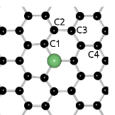
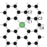
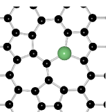
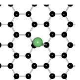
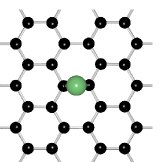


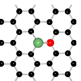
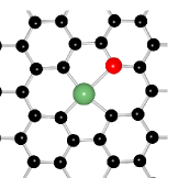
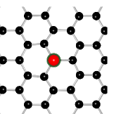
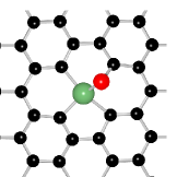
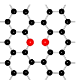


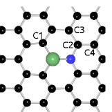
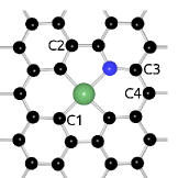
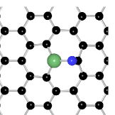
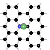
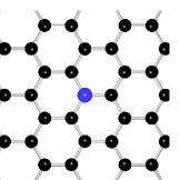


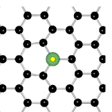
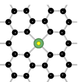
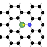
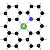
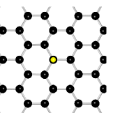
The studied defect cases and shorthand notations for labelling them are presented in Fig. 1. When a single Si, N or O atom fills a monovacancy (1Vac) in the graphene lattice, the substitutions are denoted as 1Si, 1N and 1O, and when it fills a divacancy (2Vac), the substitutions are denoted as 2Si, 2N and 2O, respectively. A composite defect consisting of two defects, for instance two substitutions, located at neighboring sites is denoted as 1Si-1O. For adatoms on pure graphene, we specify the absorption site like Si-top, and further when the adatom is on top of a defect, we combine the notation to form O-top@1Si for a oxygen adatom on top of a silicon in a monovacancy. Below, we first show the results for the defects containing only silicon and oxygen, see Figs. 1.(a)-(j). After that, nitrogen is added, see Figs. 1.(k)-(o). Finally, the hydrogen adatom cases shown in Figs. 1.(p)-(t) are studied.
II.1 Silicon and oxygen impurities
Silicon and oxygen impurities can appear in graphene for example due to contamination in growth processes where SiO2 or SiC are present, or due to purposeful post-synthesis treatment. To determine which impurities are the most likely to occur, we relaxed various silicon and oxygen point-defect atomic geometries and evaluated their formation energies.
We first analyze the results for the silicon defects. The 1Si defect, where a single carbon atom is substituted by a heavier silicon atom, prefers the tetrahedral sp3 type hybridization, resulting in an out-of-plane silicon position, as seen in Fig. 1(a). Consequently, the surrounding carbon atoms move accordingly, and the resulting curvature takes several bond lengths to relax, making it effectively a slightly extended defect. On the other hand, the silicon atom in a 2Si defect, as shown in Fig. 1(b), forms sp2d hybrid orbitals that bond with the four neighboring carbon atoms, and the geometry is only slightly perturbed in the out-of-plane direction. The defect geometries and orbital hybridizations of the 1Si and 2Si defects have been established both by computational and experimental methods in Refs. [Zhou et al., 2012a; Ramasse et al., 2013].
| Impurity atoms | Defect | Spin moment () | (Ref.) | ||
| - | 1Vac | [(C)] | Banhart et al. (2011) | ||
| 2Vac | - | Banhart et al. (2011) | |||
| Si | Isolated Si | ||||
| 1Si | - | ||||
| 2Si | - | Zhou et al. (2012b) | |||
| 1Si @ 555-777 | - | ||||
| Si-top/bridge | - | ||||
| 1Si-1Si | - | ||||
| 1Si-2Si | - | ||||
| O | Isolated O | ||||
| 1O | - | ||||
| 2O (1O-1Vac) | - | ||||
| O-bridge | - | ||||
| 1O-1O | - | ||||
| Si + O | 1Si-1O | - | |||
| 2Si-1O | - | ||||
| 1Si-2O | - | ||||
| 2Si-2O | - | ||||
| O-top @ 1Si | - | ||||
| O-bridge @ 2Si | - | ||||
| Si-bridge @ 1O | |||||
| N | Isolated N | ||||
| 1N | - | Zhou et al. (2012b) | |||
| 2N (1N-1Vac) | - | ||||
| N-bridge | [(N)] | ||||
| (3rd-NN) | - | ||||
| Si + N | 1Si-1N | [(Si), (N)] | |||
| 2Si-1N | - | Zhou et al. (2012b) | |||
| 1Si-2N | - | ||||
| 2Si-2N | |||||
| N-bridge @ 1Si | - | ||||
| N-bridge @ 2Si | [(Si), (N)] | ||||
| Si-bridge @ 1N | [(Si), (N)] | ||||
| H | Isolated H | ||||
| H-top | [(H)] | ||||
| Si + H | H-top @ 1Si | - | |||
| H-top @ 2Si | - | ||||
| N + H | H-top @ 1N | - | |||
| Si + N + H | H-top(Si) @ 1Si-1N | - | |||
| H-top(N) @ 1Si-1N | - | ||||
| H-top(Si) @ 2Si-1N | - | ||||
| H-top(N) @ 2Si-1N | - |
The defect formation energies are listed in Table 1. The 1Si and 2Si defect formation energies are eV and eV, respectively, based on the supercell calculation. Increasing the supercell size typically lowers the formation energy, except in some cases where the computational supercell is too small, such that there is not enough space for bulk graphene between the defects, or due to other finite size effects Kotakoski et al. (2006). The chosen chemical potentials affect the absolute values of the formation energies, but when comparing the formation energies of defects with the same number of atoms , the terms cancel in Eq. (1). Therefore, regardless whether the silicon atom migrates from the substrate or arrives as part of a molecule exposed to the surface, as long as the source of the silicon remains the same, 2Si has a higher formation energy than 1Si by eV. The leftover carbon atoms are assumed to form bulk graphene, but if they obtained an energy higher than , 1Si would become even more favorable compared to 2Si. On the other hand, if the defects were to form on the spot, the energy per ejected carbon atom is lower for 2Si. In any case, the sp3 hybridization in 1Si with three-fold coordination is energetically preferred to the sp2d hybridization in 2Si with four-fold coordination, even if the 1Si defect causes a local curvature of the graphene sheet.
A divacancy can be relaxed further by a bond rotation to obtain a 555-777 defect with even lower energy Banhart et al. (2011). We studied the case where a silicon atom substitutes one of the carbon atoms at the 555-777 defect. It turned out that silicon atom prefers to substitute not the middle site but a site neighboring it, as shown in Fig. 1(c). However, the formation energy of such a defect is much higher than that of 1Si and 2Si.
A silicon adatom on pristine graphene takes a position on top of a carbon atom (Si-top), but it is slightly shifted towards the hexagon of the graphene backbone, see Fig. 1(d). Its formation energy is eV, being between the 1Si and 2Si formation energies. It is only barely lower than the formation energy of an isolated silicon atom that is eV. Moreover, the total energy of the silicon adatom in a bridge position on top of a carbon-carbon bond (Si-bridge), shown in Fig. 1(e), is only a few meV higher, further indicating that silicon adatoms are rather mobile on graphene. This, in turn, implies that silicon adatoms are easily trapped by monovacancies and divacancies, because the formation energies of 1Si or 2Si are much lower than the sum of the formation energies of an isolated silicon atom or Si-top/bridge, and 1Vac or 2Vac. The energy gain is roughly - eV. Furthermore, a system consisting of a pair of neighbouring 1Si defects (1Si-1Si), or a pair of neighbouring 1Si and 2Si defects (1Si-2Si), has a total energy that is eV, or eV, lower than the energy of two fully separated defects, respectively. Such composite defects minimize the total distortion, such as the curvature of the graphene lattice, and therefore reduce the total energy. However, silicon substitution defects are not expected to be mobile (at least under ambient conditions) after they have been formed.
Oxygen could also play an important role in forming impurities in graphene. It is ubiquitous, and it is commonly present during the graphene growth process or measurements especially on a SiO2 substrate. Oxygen in graphene prefers the bridged adatom position (O-bridge, not shown) as opposed to filling a monovacancy or a divacancy, 1O or 2O (not shown). Namely, the formation energy of an O-bridge is about eV smaller than those of 1O and 2O, and also about eV smaller than the case where the oxygen adatom is located exactly on top of a carbon atom. Contrary to silicon, an oxygen atom is too small to completely fill a divacancy, and a 2O defect is better described as 1O-1Vac. Curiously, two neighbouring oxygen substitutions (1O-1O), shown in Fig. 1(j), has a remarkably low formation energy of eV. However, there can be a high energy barrier to reach such a configuration, as hinted by the high formation energy of 2O (1O-1Vac) that is eV.
It is not a surprise that, when considering composite defects containing both silicon and oxygen, silicon prefers to form 1Si and 2Si defects, and oxygen prefers the adatom position. However, the lowest formation energy of eV is obtained for an oxygen adatom located on top of a 1Si defect (O-top @ 1Si), shown in Fig. 1(h), and not in a bridged position. The oxygen adatom bonds with the silicon atom in 1Si much more preferably than with graphene, and surprisingly, also more preferably than forming an O2 molecule. An oxygen bridge located on a 2Si defect (O-bridge @ 2Si), shown in Fig. 1(i), also has an unexpectedly low formation energy of eV. These results indicate that oxygen is captured at the silicon impurities.
When embedding oxygen in the graphene lattice, the composite defects such as 1Si-1O and 2Si-1O, shown in Fig. 1 (f) and (g), have comparably small formation energies as well, eV and eV, respectively. Thus it costs less energy to form oxygen substitutions next to 1Si or 2Si than in pristine graphene. There are many possible configurations that could be called 1Si-2O or 2Si-2O, but they all have systematically at least about eV higher energies than 1Si-1O and 2Si-1O. The same goes for reversing the roles of silicon and oxygen, namely a defect consisting of a silicon adatom located near a 1O defect has a much larger formation energy. Otherwise, the silicon and oxygen pair well to form composite point-defects.
II.2 Nitrogen doping and finite spin moments
A nitrogen impurity in graphene dopes its surroundings, which can be used to tune the electronic properties of graphene. A nitrogen substitution defect (1N), shown in Fig. 1(o), is energetically by far the most stable defect configuration that contains nitrogen only. The differences in formation energy to a bridged nitrogen adatom (N-bridge, not shown) and to a divacancy substitution (2N or 1N-1Vac, not shown) are eV and eV, respectively. Since a nitrogen atom has one more electron than a carbon atom, and a substitutional nitrogen atom forms sp2 hybridized bonds in graphene, some of the electron density is donated to the nearby atoms, effectively doping the neighbourhood Lambin et al. (2012). Thus, we are mostly interested in the 1N-doped silicon impurities, to find how the added nitrogen impurity changes the properties of the silicon point-defects.
The straightforward case, with neighboring silicon and nitrogen substitutions (1Si-1N), shown in Fig. 1(k), has a comparably low formation energy of eV. Interestingly, even if neither 1Si or 1N is magnetic individually, the 1Si-1N defect has a finite total spin moment of . Table 1 also shows the atom-projected Hirshfeld spin moments, indicating that almost half of the total spin density resides near the silicon atom. This is explained by that the odd electron originating from the nitrogen atom cannot pair and forms a spin-polarized impurity state centered around the silicon atom. The nitrogen doping does not distort the atomic structure especially much compared to the 1Si case, suggesting that the silicon still hybridizes as sp3. In fact, as the nitrogen atom is able to form sp2 bonds, the 1Si-1N defect is comparable to the 1Si defect with the distinction of the nitrogen doping. Thus, in a sense, the 1N defect dopes the 1Si defect and creates a magnetic moment. However, the difference in the total energies of the spin-polarized and spin-unpolarized solutions is rather small, meV in the supercell, meaning that one has to reach low temperatures not to mix these states.
The nitrogen doped 2Si defect, namely 2Si-1N shown in Fig. 1(l), does not have a finite spin moment. However, its formation energy is extremely low, eV, which is eV lower than that of the 1Si-1N defect. Furthermore, the 2Si-1N defect is relaxed perfectly in-plane, unlike the 2Si defect. Both the 1Si-1N and 2Si-1N defects have been observed in experiments Zhou et al. (2012a, b), reflecting the fact that their formation energies are low in comparison to any competing defects. In addition, Zhou et al.Zhou et al. (2012b) evaluated the energies required to remove either the silicon or the nitrogen atom from the 2Si-1N configuration, obtaining the high values of eV and eV, respectively, which further highlights the stability of these defects.
Besides the 1Si-1N defect, some of the nitrogen-doped defects are magnetic, such as the bridged nitrogen adatoms on graphene (N-bridge, not shown) and on 2Si (N-bridge @ 2Si, not shown), and even a silicon bridge on 1N (Si-bridge @ 1N), shown in Fig. 1(n). Curiously, a nitrogen bridge on 1Si (N-bridge @ 1Si), shown in Fig. 1(m), is not magnetic even if a nitrogen bridge on graphene is. However, all their formation energies are higher than those of 1Si-1N and 2Si-1N, but still lower than having the adatoms moved on graphene. In this sense, nitrogen and silicon adatoms are attracted to 1Si, 2Si and 1N impurities, and then they are possibly relaxed to 1Si-1N and 2Si-1N defects.
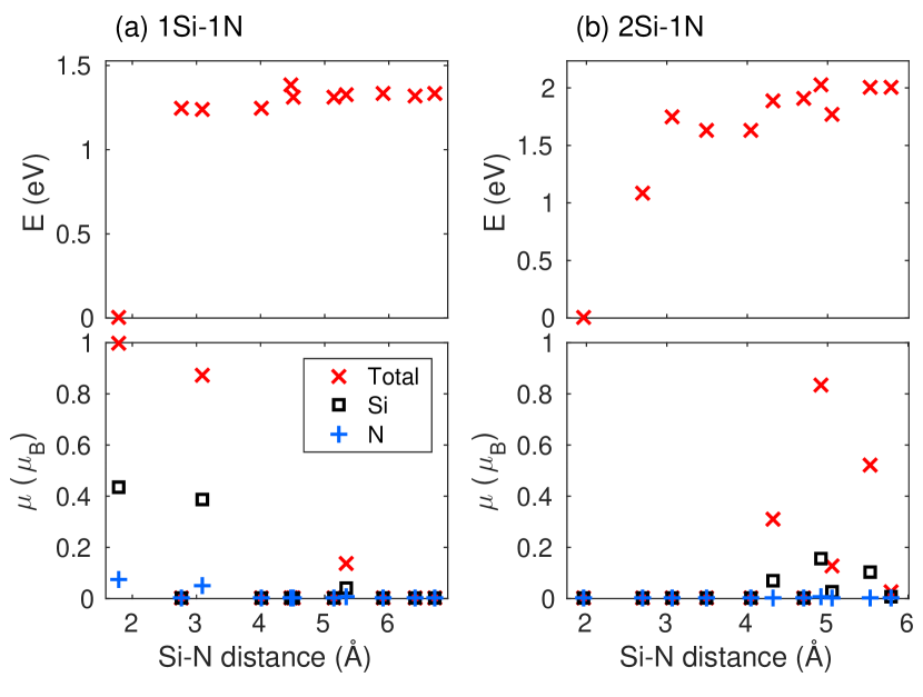
We further tested both the 1Si-1N and 2Si-1N defects by separating the silicon and nitrogen atoms from the nearest-neighbor sites. In practice, the nitrogen atom was swapped with a carbon atom farther away in the lattice, after which the geometry was fully relaxed. The resulting total energies are shown in Fig. 2 (top) as a function of the distance between the silicon and nitrogen atoms. For both 1Si-1N and 2Si-1N, separating the silicon and nitrogen atoms costs more than eV in energy. Intuitively, the 1Si and 1N defects being in the nearest-neighbor sites causes the least amount of distortion in the honeycomb lattice and there is only minimal associated energy cost. This also validates the nearest-neighbor configurations 1Si-1N and 2Si-1N as the most stable, and therefore the most important to study. In the large Si-N distance limit, the energies in Fig. 2 approach the formation energies of separated 1Si and 1N, and 2Si and 1N defects, namely the values eV and eV, respectively. In this sense, 1Si and 2Si defects separated by more than about from a 1N defect can already be considered almost fully separated in terms of the energetics.
The total and atom-projected Hirshfeld spin moments for the defect configurations with the separated silicon and nitrogen defects are shown in Fig. 2 (bottom). The systems with 1Si and 1N defects are magnetic practically only if the silicon and nitrogen atoms reside as the nearest- or third-nearest neighbors. On the other hand, the 2Si and 1N defect configurations obtain finite spin moments only if the silicon and nitrogen atoms are farther than about away from each other. However, as the separation distance grows, it is expected that the system becomes spin-unpolarized, as in the case of individual 2Si and 1N defects.
Since the 1Si-1N defects are magnetic, it is meaningful to ask how the defect spin moments interact and align in a system with many such defects. To study this, we put two 1Si-1N defects in a supercell such that the defects formed a honeycomb superlattice of their own. Based on calculations using the default light basis for each atom, due to the large number of possible configurations, it turned out that the 1Si-1N defects prefer antiferromagnetic ordering, regardless of which sublattices the impurity atoms reside on, and whether the defect out-of-plane positions are in the same direction or not. The antiferromagnetic ordering is consistently tens of meV lower in energy compared to the ferromagnetic or spin-unpolarized solutions. The energy differences are rather small, and the spin moments can be assumed to interact only weakly especially in low defect concentrations.
II.3 Hydrogen adatoms on silicon impurities
Interestingly, hydrogen adatoms located on top of silicon and silicon-nitrogen impurities have remarkably low formation energies, see Table 1. Hydrogen adatoms on graphene (H-top), shown in Fig. 1(t), have an energy penalty of eV per hydrogen atom, when using a H2 molecule as a reference for the chemical potential in Eq. (1). However, the formation energies of silicon impurities actually decrease when a hydrogen adatom is added on top the silicon impurity. The decrease in energy is the most notable for the 1Si and 1Si-1N defects, being eV and eV, respectively. The 1N-doping plays a significant role by lowering the energy even further, even though the hydrogen adatom is clearly located on top of the silicon atom, see Fig. 1(p) and (s). The low formation energies overall hint that the silicon-nitrogen defects could be reactive not only to hydrogen but also to various molecules as well. This is the prerequisite for using the defects as sensors.
A hydrogen adatom on graphene has a total spin-moment of . This follows from the fact that the hydrogen atom bonds to a carbon atom, passivating the carbon orbital and effectively resulting in an empty site as seen from the point of view of the electron bands. By Lieb’s theoremLieb (1989), a finite spin moment will result from the sublattice imbalance. Quite surprisingly, magnetization does not occur when the hydrogen adatom is located on top of a 1Si defect, or a 1Si-1N defect. In fact, all the silicon and silicon-nitrogen impurities with a hydrogen adatom considered here, see Table 1, are nonmagnetic. Therefore hydrogen adatoms, which readily trap at the silicon and silicon-nitrogen impurities, passivate any defect-induced magnetism.
II.4 Electronic band structures

In the following, we studied the DFT band structures and DOS of systems with unit cells of graphene that contain a single 1Si, 2Si, 1Si-1N, or 2Si-1N defect. This corresponds to an infinite, periodic array of the impurities. The band energies are evaluated in the reciprocal space along the line segments between the nearby high symmetry points in the first Brillouin zone (BZ), as illustrated in Fig. 3. From the outset, we restricted the study only to one of the halves of the first BZ, since time reversal symmetry is not broken, and therefore inversion around the point, namely , does not alter state energies. This also holds for the majority and minority spin channels in the spin-polarized case.
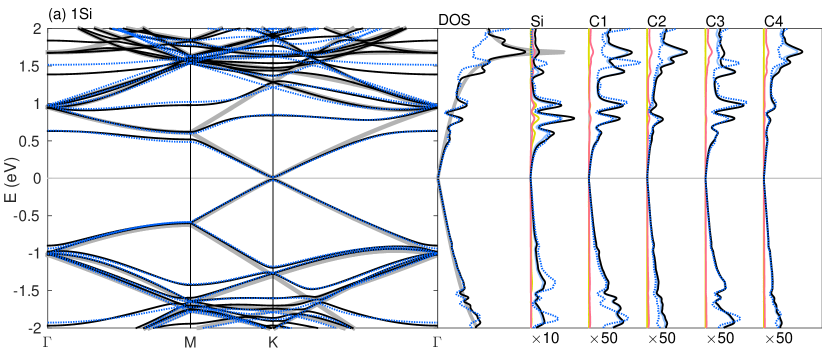
The band structure, DOS and atom-projected partial DOS (pDOS) of the system with a 1Si defect are shown in Fig. 4(a). The band structure closely matches the pristine graphene band structure (thick grey line). In fact, one sees in the presented energy range the pristine graphene occupied and unoccupied electron bands that have been folded multiple times in order to match the supercell as a periodic unit. A supercell with a defect cannot be unfolded back into smaller periodic unit cells, as there are energy gaps between the bands at the high symmetry points. Curiously, with supercells of sizes where is divisible by three, the and points are actually mapped onto the point, and there would be no energy gap at Lambin et al. (2012); Martinazzo et al. (2010). However, in our case with , there is a small energy gap at the point in the 1Si band structure, but otherwise the Dirac cone seems to be unperturbed.
Consequently, the 1Si DOS is similar to the graphene DOS, indicated by the thick grey line in Fig. 4(a), except that there are additional states at energies around eV. The opening of energy gaps in the band structure results in double peaks in the DOS if the peak broadening is sufficiently small. But most importantly, the peaks in the DOS are in general explained by the flatter energy bands, for instance resulting from localized impurity states that are only weakly -dependent. However, substituting a carbon atom by a valence isoelectronic silicon atom does not introduce a new impurity band, but rather the electron bands become perturbed. Peaks are then formed as there are stronger resonances at certain energies that are also expected to depend on the dimensions of the periodic array of defects. The pDOS around the 1Si defect, in Fig. 4(a), shows that the peaks in the density at around eV are mostly localized at the silicon atom and the nearest and third-nearest carbon atoms C1 and C3, see Fig. 1(a) for the atom labels. We can also see that carbon atoms exhibit only p-type orbital occupations as expected, but the silicon atom has some contribution from s- and even d-type orbitals.
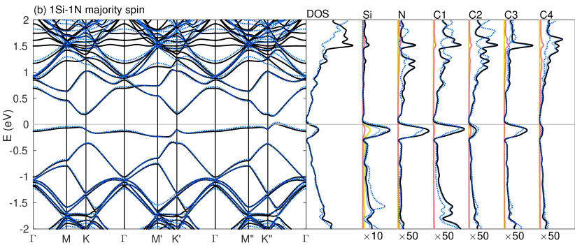
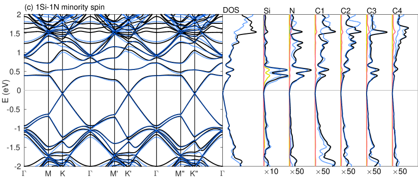
The 1Si-1N band structure and DOS are shown in Fig. 1(b) and (c) for the majority and minority spin components from a calculation with collinear spin. The paths in the reciprocal space along which the band energies are shown now include the three triangular paths , , and due to breaking of the graphene lattice symmetries. There is a spin moment of that corresponds to an almost fully occupied band in the majority spin channel that is unoccupied in the minority spin channel. The origin of the spin moment is the nitrogen atom that introduces the odd electron that is attracted to the silicon atom. As a consequence, there is an almost flat impurity band just below the Fermi energy, and a clear bump in the DOS and atom-projected pDOS. The density is mostly localized at the silicon atom with some weight also at nearby atoms of the adjacent sublattice. In addition to the p-type orbital occupations, the impurity state also exhibits some s- and d-type orbital occupation at the silicon atom, and small d-type occupations even at the second-nearest neighbor carbon atom C2.
For both spin components, the band energies along the three paths , and have only minor differences, suggesting that there is no strong directional dependence. Therefore, the electronic states at the nitrogen atom are expected to be similar to the states at the carbon atoms that are nearest-neighbours of the silicon atom. In fact, the band structure of the minority spin component, shown in Fig. 1(c), closely resembles the band structure of the 1Si defect. The Dirac cone at the -point is intact, being only slightly shifted to the occupied side due to the nitrogen doping. However, with the larger system of graphene unit cells, the spin moment is already , and therefore the Dirac cone in the minority channel is expected at the Fermi energy. We can call such a material half-semimetal, since the majority spin channel has only an impurity band just below the Fermi energy, and the band structure of the minority spin channel is that of a semimetal. Furthermore, the main qualitative difference between the pDOS of periodic arrays of 1Si and 1Si-1N defects is that the silicon pDOS shows two peaks in the 1Si-1N minority channel, whereas the silicon pDOS at the 1Si defect has three peaks. Moreover, there is no clear occupation of d-type orbitals in the minority channel of the 1Si-1N defect system.
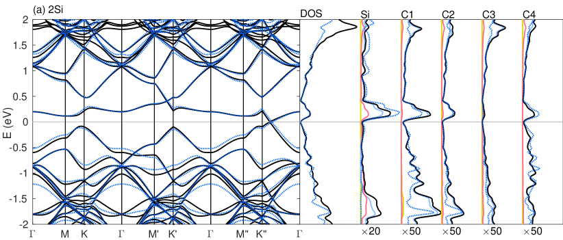
The band structure, DOS and pDOS of a system with a 2Si defect are shown in Fig. 5(a). The breaking of the sublattice and the three-fold rotational symmetries have a profound effect on the band structure. Namely, there is a strong directional dependence on the wave vectors , and even the Dirac cones are slightly shifted from the , and points. Furthermore, there is a clear bump in the DOS roughly at eV. This shows in the pDOS as localized density from p- and d-type orbitals at the silicon atom and as density from p-type orbitals at the nearby carbon atoms. Interestingly, there are states in the occupied side that do not have much density at the silicon atom, but they do have density at the nearby carbon atoms. Therefore there are also impurity states surrounding the silicon site.
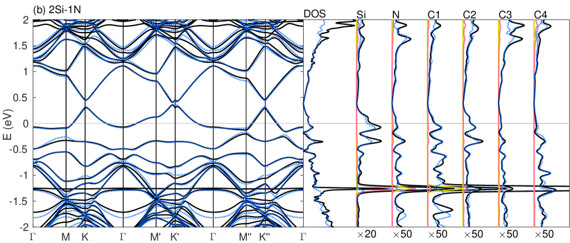
The band structure of a system with a 2Si-1N defect, shown in 5(b), is necessarily doped due to the odd electron from the nitrogen atom. There is a band at the Fermi energy that is half filled, and as a result the conical dispersions are shifted roughly by eV to the unoccupied side. In fact, the 2Si-1N band structure looks more like doped 1Si band structure than 2Si band structure. Compared to 2Si band structure, where the bands have strong directional dependency, the valence bands in the 2Si-1N band structure are almost flat resulting in many distinct peaks in the DOS and pDOS in the defect neighborhood. These states are again not only localized impurity states at the silicon but also at the nearby carbon atoms, especially the nearest-neighbour carbon atom C1. Curiously, there is an almost perfectly flat band at eV, implying a state localized at the defect, and that the related orbitals have a symmetry other than that of the electrons.
III Tight-binding results
III.1 Tight-binding models
We constructed tight-binding models for the silicon and silicon-nitrogen point-defects on graphene to further study their electronic and transport properties. This way we could simulate larger systems with random defect configurations, which is beyond typical first principles approaches.
The tight-binding model with an orthogonal state per each atom site, and simple hoppings between the sites, describes the graphene and electron bands remarkably well Wallace (1947); Castro Neto et al. (2009). The tight-binding Hamiltonian is written as
| (2) |
where () creates (annihilates) a fermion in a state , and H.c. stands for Hermitian conjugate. Here, the coefficients describe on-site potentials, and are hoppings between sites. We denote as the nearest-, second-nearest-, and third-nearest neighbor hoppings, respectively.
The tight-binding models for systems containing defects were found by modifying the hoppings and on-site potentials in the vicinity of the defects, and fitting the outcome to the first principles band structures. Furthermore, we checked that the resulting tight-binding local density of states (LDOS) matched the first principles atom-projected partial DOS around the Fermi energy, at least qualitatively. We used the supercells that have a single defect each. The band structure fitting was performed in the first Brillouin zone in a uniform grid of k-points. We took 12 bands into the fitting procedure, the six highest valence bands and the six lowest conduction bands, determined at the point, except for the 2Si-1N defect, where only four valence and four conduction bands were taken in order to avoid the flat band at eV.
III.2 Tight-binding parametrization
First the carbon-carbon (C-C) hoppings were obtained by fitting to the pristine graphene band structure. We allowed and to be free fitting parameters to scale the unit of energy and to freely break the electron-hole symmetry by tuning . We included the third-nearest neighbor hoppings by assuming that , where the factor is motivated by previous graphene tight-binding models Hancock et al. (2010). If was not constrained, altering and simultaneously would produce a continuous set of models with good fits. The resulting C-C hoppings are eV, which were used for all carbon-carbon hoppings in our tight-binding calculations.
We expect that the properties of both the silicon and silicon-nitrogen defects can be reproduced around the Fermi energy using simple tight-binding models. Namely, silicon and carbon atoms are valence isoelectronic, and nitrogen is also able to form sp2 bonds. The relevant and electron bands are then perturbed by the defects in the effective tight-binding description. Moreover, we chose a minimal set of tight-binding parameters to enhance the physical significance of each parameter. We took only the nearest-neighbor hoppings between the Si and C atoms, and between the Si and N atoms, to be nonzero. The hoppings between C and N atoms were taken identical to those of the C-C hoppings, which is similar to the nitrogen substitution model in Ref. Lambin et al., 2012. The C on-site potentials were set to zero, whereas the Si and N on-site potentials could take non-zero values.
| Defect | Spin polarization | Hopping : | Potential : | ||
|---|---|---|---|---|---|
| C-Si | Si-N | Si | N | ||
| 1Si | no | ||||
| 1Si-1N | majority | ||||
| minority | |||||
| no | |||||
| 2Si | no | ||||
| 2Si-1N | no | ||||
With the parameter constraints and fitting method described above, the resulting tight-binding parameters for the 1Si, 1Si-1N, 2Si, and 2Si-1N defects are listed in Table 2. We provide spin-unpolarized and spin-polarized parametrization of the 1Si-1N defect with distinct models for the majority and minority spin components. Comparing to first principles, the tight-binding models produced remarkably accurate band structures, DOS, and LDOS, as shown by the dotted lines in Figs. 4 and 5. The tight-binding Fermi energies are at eV, eV, eV, and eV for the systems with a 1Si, 1Si-1N (spin-polarized), 2Si, and 2Si-1N defect, respectively. Below, we use these values as point, even if the defect concentration changes.
The most visible signature of the 1Si defect is the opening of the energy gaps between the lowest and second lowest conduction bands at the point, as well as between the second and third lowest conduction bands at the and points. This can be explained by the weaker Si-C hopping compared to the C-C hopping value. An on-site potential at the silicon atom also breaks the translational symmetry, resulting in small energy gaps at many band crossings. In the case of the 2Si defect, the C-Si hopping is even weaker, and we set a repulsive on-site potential at the silicon atom, since the sp2d hybridization takes more electrons to form bonds with the four neighboring carbon atoms. For the defects containing nitrogen, we used a rather low on-site potential at the nitrogen sites, because a nitrogen substitution dopes its surroundings by sharing some of its electron density. For the 2Si-1N defect, we did not include the state corresponding to the extremely flat band in the model.
Curiously, a 1Si-1N defect is spin-polarized. We obtained the tight-binding Hamiltonians for both the majority, , and the minority, , spin components individually. To explicitly include the electron spin in the Hamiltonian, we can write
| (3) |
where the electron spin is first projected onto the defect majority and minority spin states, and , and we have defined , , and . Due to the last term in the Hamiltonian, the electron spin can flip, if it is not aligned with the defect spin moment. The strength of the spin flipping is proportional to the difference of the majority and minority tight-binding parameters of . In our case, the tight-binding models for the two spin components are not necessarily consistent by e.g. assuming a mean-field Hubbard model, see Ref. [Soriano et al., 2011], where only the on-site potentials can be spin-dependent. However, the obtained majority, minority and spinless tight-binding models for the 1Si-1N defect are reasonable in a sense that the parameters are qualitatively similar, and the values of the spinless parameters are somewhere between the values of the majority and minority parameters. Furthermore, it seems that at least the C-Si hopping needs to be slightly spin-dependent in order to obtain a qualitatively good fit of the band structures.
III.3 Randomly positioned defects
The tight-binding models constructed above can be used to study large systems containing millions of atoms, much larger than what can be treated by state-of-the-art first principles simulations. The large system sizes are needed to eliminate finite-size effects. Below, we study the electronic and transport properties of supercells with atoms in total and with randomly placed defects at a defect concentration of . Moreover, we take ensemble averages over several defect configurations to ensure that the results are converged in the large system limit. It is, however, sufficient to average over only roughly five defect configuration realizations, as the systems considered here are large enough for much of the random fluctuations to average out.
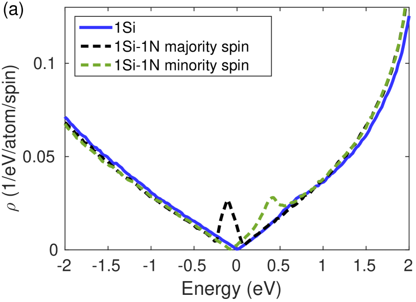
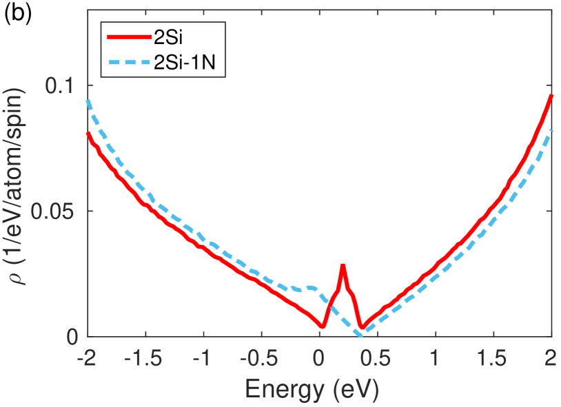
The DOS of such large systems with randomly placed 1Si, 1Si-1N, 2Si and 2Si-1N defects are shown in Fig. 6. There is a strong similarity to the DOS of a periodic supercell with one defect presented in Figs. 4 and 5. However, averaging over random defect configurations smoothens the individual peaks of the periodic case, and one obtains the characteristic features of the DOS. Still, of course, the band structure of the periodic supercell and the DOS of a large system are closely related: whenever there are relatively flat impurity bands, there are impurity states at the corresponding energies, manifesting themselves as humps in the DOS.
It is surprising that the DOS of a system containing of 1Si defects shows only a very weak deviation from the DOS of pristine graphene, whereas both the majority and minority spin channels of the 1Si-1N defect exhibit clear peaks. Namely, the resonant impurity states of the majority (minority) spin reside on the occupied (unoccupied) side, at negative (positive) energies. Similarly, the resonant impurity states of the 2Si defects correspond to positive energies. The 2Si-1N defect DOS in Fig. 6(b) is again only weakly perturbed from the pristine graphene DOS, but it is clearly doped by the nitrogen substitutions. It seems that the spiky DOS of the periodic defect case, as shown in Fig. 5(b), smoothens to a slight elevation around eV.
III.4 Electronic transport
The tight-binding models also enabled us to perform transport calculations with large system sizes. We used the real-space Kubo-Greenwood method (RSKG) Mayou (1988); Mayou and Khanna (1995); Roche and Mayou (1997); Triozon et al. (2002) which scales linearly with respect to the total number of atoms and allows for the simulation of truly two-dimensional graphene with many randomly distributed defects. Our implementation is significantly accelerated by using graphics processing units (GPUs) Fan et al. (2014a).
The RSKG method can be used to efficiently compute the intrinsic conductivity as a function of the Fermi energy and correlation time . In most cases, the maximum of over represents a good approximation of the semiclassical conductivity . The semiclassical conductivity is the conductivity of a system where quantum-mechanical interference phenomena leading to weak and strong localization are suppressed. The elastic mean free path can be then calculated using the Einstein relation for diffusive transport
| (4) |
where is the Fermi velocity and is the total DOS.
In systems with some given defect type, both the semiclassical conductivity and the elastic mean free path depend on the defect concentration . Here, was set to match the silicon concentration, and it is fixed to . The defects were positioned and oriented randomly in the graphene lattice, as would be expected in real materials.
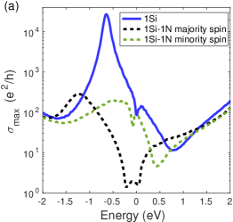
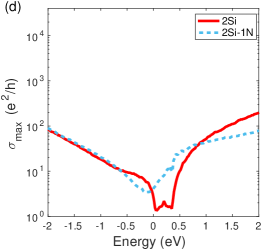
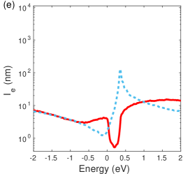
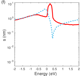
The defects act as resonant scatterersNi et al. (2010) that limit the charge carrier conduction around the resonant energies, resulting in local minima in the semiclassical conductivity. The semiclassical conductivities for systems with many randomly positioned 1Si and 1Si-1N defects are presented in Fig. 7(a) and with many randomly positioned 2Si and 2Si-1N defects in Fig. 7(d). The system with 1Si defects is again closest to pure graphene, showing a weak minimum only around eV. Furthermore, the peak at eV should be even more singular than Fig. 7(a) shows, because in our simulation the intrinsic conductivity was still increasing at the largest correlation times considered. For the spin-polarized 1Si-1N defects, Fig. 7(a) shows the semiclassical conductivity separately for the majority and minority tight-binding models. Using the same model to describe all defects corresponds in this case to the ferromagnetic ordering of the defect spin moments that would point along the direction of an external field. Both spin channels have smaller semiclassical conductivities at energies that match the peaks in their respective DOS. Then, similarly to the DOS, the conductivities of the spin channels are completely different around zero energy, suggesting that ferromagnetically ordered 1Si-1N defects would lead to distinct transport properties that depend on the spin states of the charge carriers. The 2Si and 2Si-1N defects exhibit clearly smaller semiclassical conductivities than the 1Si and 1Si-1N defects, and the minima in conductivity are again found at energies that match the peaks in the DOS.
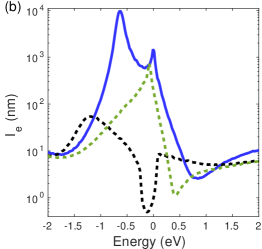
From the semiclassical conductivity, we could calculate the elastic mean free path , shown in Fig. 7(b) and (e). For the 1Si case, the smallest values of are around a few nanometers while the system with 1Si-1N defects exhibits values that are even smaller than 1 nm for a single spin channel. Thus the 1Si-1N defect is a strong scatterer of the charge carriers. Interestingly, the difference between the spin channels is very large around zero energy, being around three orders of magnitude. The systems with 1Si defects, on the other hand, exhibit elastic mean free paths that exceed one micrometer, which is a surprising result for such a high defect concentration of . The elastic mean free paths in systems with 2Si and 2Si-1N defects are rather short in the energy window shown in Fig. 7(e), as expected based on the low conductivities.
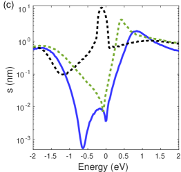
To quantify the transport properties with any small value of defect concentration Uppstu et al. (2012), we calculated the scattering cross section. After is obtained for a given concentration , the effective scattering cross section with dimension of [length] in two dimensions is evaluated as Uppstu et al. (2012)
| (5) |
where is the 2D number density of the defects, and is the carbon-carbon distance. For relatively small , which is often the case in real experiments, is largely independent of .
The scattering cross sections are shown in Fig. 7(c) and (f). The large values of the scattering cross section for one spin channel in systems with 1Si-1N defects demonstrate further that the scattering by this defect type is highly spin-dependent. In general, the scattering cross section shows that the silicon and silicon-nitrogen defects scatter charge carriers in clearly distinct ways. The 1Si defects cause barely any scattering below eV and scatter moderately at around eV, whereas the 1Si-1N defects scatter the majority spin charge carriers very strongly at eV and the minority spin charge carriers moderately at eV. In the 2Si case, scattering is very strong between eV and eV where, in turn, the 2Si-1N defects cause only little scattering.
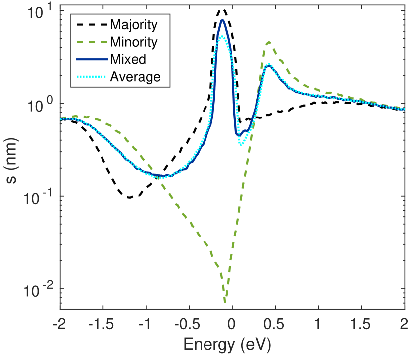
So far we have shown the transport results for ferromagnetically ordered 1Si-1N defects, where all the impurity spin moments point in the same direction. In this case, the charge carrier spin basis can be chosen to align with the impurity spins, and the majority and minority spin components can be solved independently. On the other hand, when the external field is weak, the 1Si-1N defects prefer antiferromagnetic ordering. However, the interaction energies between defect spin moments are rather small, roughly tens of meV, and the temperatures in experiments might not be low enough to manifest clear magnetic ordering, leading to random orientations of the impurity spin moments. The charge carrier spin basis cannot be simultaneously aligned with many random impurity spin moments, which can lead to processes where the spin of the charge carrier flips in a scattering event. These might be relevant for spin relaxation in graphene Kochan et al. (2014).
Our RSKG implementation does not allow impurity spins to point in random directions, but we were able to simulate the case where the defects are positioned randomly in the graphene lattice, and each impurity spin is randomly taken to point either up or down. This corresponds to assigning the majority or the minority model for each defect randomly. In a sense, this can be called antiferromagnetic ordering of the defects, even though antiferromagnetism is not enforced locally. The scattering cross section in this case with mixed 1Si-1N majority and minority defects, labelled as “mixed”, is shown in Fig. 8. Scattering occurs now at both resonances from the majority and minority DOS, as one would naturally expect. Furthermore, the results show that one can average the scattering cross sections of the two spin channels to obtain a total scattering cross section that is in good agreement with the “mixed” case. This is a special case of Mathiessen’s rule, with equal defect densities of two defect types.
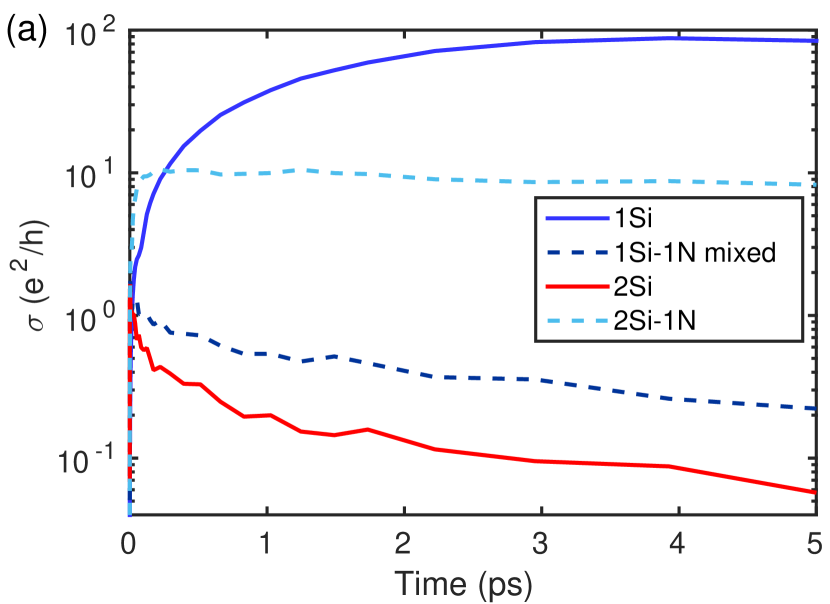
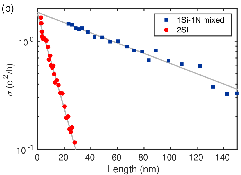
The defects considered here break the graphene sublattice symmetry. Therefore pseudospin is not conserved, and backscattering is allowed. Localization effects are thus expected to occur at low temperatures in large systems with sufficiently large defect concentrations. The conductivities for the 1Si-N and 2Si defects at eV and at eV, respectively, shown in Fig. 9(a), are small and decrease as a function of correlation time. This indicates the presence of strong localization around the charge neutrality point (CNP), where the semiclassical conductivities are close to the so-called “minimum conductivity” . Converting the correlation time to length Uppstu et al. (2014), and omitting the initial region of increasing conductivity that corresponds to the transition from ballistic to diffusive transport, we obtain the length dependence shown in Fig. 9(b). Clearly, the conductivity decays exponentially as , where the 2D localization lengths can be estimated to be nm for the 1Si-1N defects and nm for the 2Si defects at a defect concentration of .
In systems with 1Si and 2Si-1N defects, the semiclassical conductivity is large at eV and at eV, respectively, as seen in Fig. 9(a), which implies that the corresponding 2D localization lengths, which are exponentially proportional to the semiclassical conductivity Fan et al. (2014b), are also large, presumably much larger than the phase coherence lengths in real systems. Therefore strong localization is not expected to occur. However, for the 2Si-1N defects we can see weak localization, characterized by the slight decrease of the conductivity as a function of the correlation time, which is most clear around eV (not shown). At this point, the estimated 2D localization length is of the order of nm at a defect concentration, and it would be even larger with a smaller defect concentration. In conclusion, the localization effects do not play an important role in systems with 1Si and 2Si-1N defects in real physical systems, whereas strong localization around the CNP is predominant for the 2Si and 1Si-1N defect types.
Conclusions
By systematically optimizing the geometry of various defects in graphene containing silicon, nitrogen, oxygen, and hydrogen atoms, we have identified the defect types with the lowest formation energies. Namely, silicon and nitrogen prefer to fill a monovacancy in graphene, whereas oxygen and hydrogen clearly favor to stay on top of the graphene plane as adatoms. In general, various impurities are effectively attracting each other to minimize the overall distortion of the graphene backbone. In this sense, nitrogen, oxygen, and hydrogen impurites and adatoms are trapped to silicon impurities.
To study the electronic properties of silicon and silicon-nitrogen impurities, we have focused on defects where a silicon atom fills a monovacancy (1Si) or a divacancy (2Si). Energetically the most reasonable way to dope the 1Si and 2Si defects by nitrogen is to substitute a nearest-neighbour carbon atom of the silicon atom with a nitrogen atom, denoted as 1Si-1N and 2Si-1N. Such nitrogen doping changes the electronic properties of the defects remarkably, most notably resulting in defect-induced finite spin moments in the case of 1Si-1N defects. Each 1Si-1N defect has a spin moment of that is mainly localized at the neighbourhood of the silicon atom. The spin moments of the 1Si-1N defects interact with each other preferring antiferromagnetic ordering. It also turns out that hydrogen adatoms quench any finite spin moments of the silicon-nitrogen defects, further enabling the use of such defects in spintronic devices.
We have derived tight-binding models to describe the 1Si, 2Si, 1Si-1N, and 2Si-1N defects in graphene, and to evaluate electronic transport properties in realistic systems with millions of atoms containing many randomly placed impurities. The effective scattering cross sections have been calculated to describe the intrinsic transport properties of systems with each of the defect types. Systems with 1Si and 2Si-1N defects have similar transport properties to pristine graphene, whereas the 1Si-1N and 2Si defects scatter charge carriers heavily close to charge neutrality. Furthermore, the spin-polarized 1Si-1N defects have strongly spin-dependent electronic transport properties. Namely, there are resonant impurity states localized at the defects in the majority spin component, whereas the minority spin component is a semimetal with similar properties to pristine graphene close to charge neutrality. Therefore the spin transport properties can be controlled by applying an external field that can tune the magnetic ordering of the defects. Furthermore, in realistically sized graphene samples, the 2Si and 1Si-1N defects are expected to cause strong localization, whereas systems with the energetically preferred 1Si and 2Si-1N defects exhibit so large localization lengths that localization effects are unlikely to be observed experimentally.
Our results provide microscopic insights into the electronic structure and transport of graphene with Si impurities and Si-N/O/H complex defects. It is possible to extend graphene functionalities by tuning its properties through controllable introduction of defects either during the growth or by using post-synthesis methods. Further exposure of silicon impurities to particular gases should give rise to other defects. On the other hand, knowing the signatures of particular types of defects in Si-doped graphene, one can use these systems in gas sensors Chen et al. (2012); Niu et al. (2013), or to design and further improve graphene-based nanodevices.
Acknowledgements.
We thank Morten Rishøj Thomsen for useful discussions. This research has been supported by the Academy of Finland through its Centres of Excellence Program (project no. 251748) as well as projects 263416 and 286279. We acknowledge the computational resources provided by Aalto Science-IT project and Finland’s IT Center for Science (CSC).References
- Novoselov et al. (2005) K. S. Novoselov, A. K. Geim, S. V. Morozov, D. Jiang, M. I. Katsnelson, I. V. Grigorieva, S. V. Dubonos, and A. A. Firsov, “Two-dimensional gas of massless Dirac fermions in graphene,” Nature 438, 197–200 (2005).
- Chen et al. (2008) Jian-Hao Chen, Chaun Jang, Shudong Xiao, Masa Ishigami, and Michael S Fuhrer, “Intrinsic and extrinsic performance limits of graphene devices on sio2,” Nature nanotechnology 3, 206–209 (2008).
- Morozov et al. (2008) S. V. Morozov, K. S. Novoselov, M. I. Katsnelson, F. Schedin, D. C. Elias, J. A. Jaszczak, and A. K. Geim, “Giant intrinsic carrier mobilities in graphene and its bilayer,” Phys. Rev. Lett. 100, 016602 (2008).
- Siegel et al. (2011) David A. Siegel, Cheol-Hwan Park, Choongyu Hwang, Jack Deslippe, Alexei V. Fedorov, Steven G. Louie, and Alessandra Lanzara, “Many-body interactions in quasi-freestanding graphene,” Proceedings of the National Academy of Sciences 108, 11365–11369 (2011).
- Castro Neto et al. (2009) A. H. Castro Neto, F. Guinea, N. M. R. Peres, K. S. Novoselov, and A. K. Geim, “The electronic properties of graphene,” Rev. Mod. Phys. 81, 109–162 (2009).
- Son et al. (2006a) Young-Woo Son, Marvin L. Cohen, and Steven G. Louie, “Energy gaps in graphene nanoribbons,” Phys. Rev. Lett. 97, 216803 (2006a).
- Yang et al. (2007) Li Yang, Cheol-Hwan Park, Young-Woo Son, Marvin L. Cohen, and Steven G. Louie, “Quasiparticle energies and band gaps in graphene nanoribbons,” Phys. Rev. Lett. 99, 186801 (2007).
- Han et al. (2007) Melinda Y. Han, Barbaros Özyilmaz, Yuanbo Zhang, and Philip Kim, “Energy band-gap engineering of graphene nanoribbons,” Phys. Rev. Lett. 98, 206805 (2007).
- Berashevich and Chakraborty (2009) Julia Berashevich and Tapash Chakraborty, “Tunable band gap and magnetic ordering by adsorption of molecules on graphene,” Phys. Rev. B 80, 033404 (2009).
- Balog et al. (2010) Richard Balog, Bjarke Jørgensen, Louis Nilsson, Mie Andersen, Emile Rienks, Marco Bianchi, Mattia Fanetti, Erik Lægsgaard, Alessandro Baraldi, Silvano Lizzit, et al., “Bandgap opening in graphene induced by patterned hydrogen adsorption,” Nature materials 9, 315–319 (2010).
- Casolo et al. (2011) S. Casolo, R. Martinazzo, and G. F. Tantardini, “Band engineering in graphene with superlattices of substitutional defects,” The Journal of Physical Chemistry C 115, 3250–3256 (2011).
- Denis (2010) Pablo A. Denis, “Band gap opening of monolayer and bilayer graphene doped with aluminium, silicon, phosphorus, and sulfur,” Chemical Physics Letters 492, 251 – 257 (2010).
- Forbeaux et al. (1998) I. Forbeaux, J.-M. Themlin, and J.-M. Debever, “Heteroepitaxial graphite on interface formation through conduction-band electronic structure,” Phys. Rev. B 58, 16396–16406 (1998).
- Singh et al. (2011) Virendra Singh, Daeha Joung, Lei Zhai, Soumen Das, Saiful I. Khondaker, and Sudipta Seal, “Graphene based materials: Past, present and future,” Progress in Materials Science 56, 1178 – 1271 (2011).
- Wang et al. (2012) Haibo Wang, Thandavarayan Maiyalagan, and Xin Wang, “Review on recent progress in nitrogen-doped graphene: Synthesis, characterization, and its potential applications,” ACS Catalysis 2, 781–794 (2012).
- Wang et al. (2014) Xuewan Wang, Gengzhi Sun, Parimal Routh, Dong-Hwan Kim, Wei Huang, and Peng Chen, “Heteroatom-doped graphene materials: syntheses, properties and applications,” Chem. Soc. Rev. 43, 7067–7098 (2014).
- Bangert et al. (2013) U. Bangert, W Pierce, D M Kepaptsoglou, Q Ramasse, R Zan, M H Gass, J a Van den Berg, C B Boothroyd, J Amani, and H Hofsäss, “Ion Implantation of Graphene-Toward IC Compatible Technologies.” Nano letters 13, 4902–7 (2013).
- Zhou et al. (2012a) Wu Zhou, Myron D. Kapetanakis, Micah P. Prange, Sokrates T. Pantelides, Stephen J. Pennycook, and Juan-Carlos Idrobo, “Direct determination of the chemical bonding of individual impurities in graphene,” Phys. Rev. Lett. 109, 206803 (2012a).
- Ramasse et al. (2013) Quentin M. Ramasse, Che R. Seabourne, Despoina-Maria Kepaptsoglou, Recep Zan, Ursel Bangert, and Andrew J. Scott, “Probing the bonding and electronic structure of single atom dopants in graphene with electron energy loss spectroscopy,” Nano Letters 13, 4989–4995 (2013).
- Zhou et al. (2012b) Wu Zhou, Jaekwang Lee, Jagjit Nanda, Sokrates T. Pantelides, Stephen J. Pennycook, and Juan-Carlos Idrobo, “Atomically localized plasmon enhancement in monolayer graphene,” Nat Nano 7, 161–165 (2012b).
- Bonaccorso et al. (2010) Francesco Bonaccorso, Z Sun, T Hasan, and AC Ferrari, “Graphene photonics and optoelectronics,” Nature photonics 4, 611–622 (2010).
- Wei et al. (2009) Dacheng Wei, Yunqi Liu, Yu Wang, Hongliang Zhang, Liping Huang, and Gui Yu, “Synthesis of n-doped graphene by chemical vapor deposition and its electrical properties,” Nano Letters 9, 1752–1758 (2009).
- Lambin et al. (2012) Ph. Lambin, H. Amara, F. Ducastelle, and L. Henrard, “Long-range interactions between substitutional nitrogen dopants in graphene: Electronic properties calculations,” Phys. Rev. B 86, 045448 (2012).
- Son et al. (2006b) Young-Woo Son, Marvin L Cohen, and Steven G Louie, “Half-metallic graphene nanoribbons,” Nature 444, 347–349 (2006b).
- Yazyev and Helm (2007) Oleg V. Yazyev and Lothar Helm, “Defect-induced magnetism in graphene,” Phys. Rev. B 75, 125408 (2007).
- Krasheninnikov et al. (2009) A. V. Krasheninnikov, P. O. Lehtinen, A. S. Foster, P. Pyykkö, and R. M. Nieminen, “Embedding transition-metal atoms in graphene: Structure, bonding, and magnetism,” Phys. Rev. Lett. 102, 126807 (2009).
- Chen et al. (2011) Jian-Hao Chen, Liang Li, William G. Cullen, Ellen D. Williams, and Michael S. Fuhrer, “Tunable Kondo effect in graphene with defects,” Nature Physics 7, 535–538 (2011).
- Lopez-Bezanilla et al. (2014) Alejandro Lopez-Bezanilla, Wu Zhou, and Juan-Carlos Idrobo, “Electronic and quantum transport properties of atomically identified Si point defects in graphene,” The Journal of Physical Chemistry Letters 5, 1711–1718 (2014).
- Cheng et al. (2014) Cai-ping Cheng, Hui-fang Hu, Zhao-jin Zhang, Quanhui Liu, Ying Chen, and Ping Peng, “Negative differential resistance induced by sinx co-dopant in armchair graphene nanoribbon,” Modern Physics Letters B 28, 1450229 (2014).
- Blum et al. (2009) Volker Blum, Ralf Gehrke, Felix Hanke, Paula Havu, Ville Havu, Xinguo Ren, Karsten Reuter, and Matthias Scheffler, “Ab initio molecular simulations with numeric atom-centered orbitals,” Computer Physics Communications 180, 2175 – 2196 (2009).
- Perdew et al. (1996) John P. Perdew, Kieron Burke, and Matthias Ernzerhof, “Generalized gradient approximation made simple,” Phys. Rev. Lett. 77, 3865–3868 (1996).
- Krasheninnikov and Nieminen (2011) A. V. Krasheninnikov and R. M. Nieminen, “Attractive interaction between transition-metal atom impurities and vacancies in graphene: a first-principles study,” Theoretical Chemistry Accounts 129, 625–630 (2011).
- Lherbier et al. (2012) Aurélien Lherbier, Simon M.-M. Dubois, Xavier Declerck, Yann-Michel Niquet, Stephan Roche, and Jean-Christophe Charlier, “Transport properties of graphene containing structural defects,” Phys. Rev. B 86, 075402 (2012).
- Wang and Pantelides (2012) Bin Wang and Sokrates Pantelides, “Magnetic moment of a single vacancy in graphene and semiconducting nanoribbons,” Physical Review B 86, 165438 (2012).
- Banhart et al. (2011) Florian Banhart, Jani Kotakoski, and Arkady V. Krasheninnikov, “Structural defects in graphene,” ACS Nano 5, 26–41 (2011).
- Kotakoski et al. (2006) J. Kotakoski, A. V. Krasheninnikov, and K. Nordlund, “Energetics, structure, and long-range interaction of vacancy-type defects in carbon nanotubes: Atomistic simulations,” Phys. Rev. B 74, 245420 (2006).
- Lieb (1989) Elliott H. Lieb, “Two theorems on the hubbard model,” Phys. Rev. Lett. 62, 1201–1204 (1989).
- Martinazzo et al. (2010) Rocco Martinazzo, Simone Casolo, and Gian Franco Tantardini, “Symmetry-induced band-gap opening in graphene superlattices,” Phys. Rev. B 81, 245420 (2010).
- Wallace (1947) P. R. Wallace, “The band theory of graphite,” Phys. Rev. 71, 622–634 (1947).
- Hancock et al. (2010) Y. Hancock, A. Uppstu, K. Saloriutta, A. Harju, and M. J. Puska, “Generalized tight-binding transport model for graphene nanoribbon-based systems,” Phys. Rev. B 81, 245402 (2010).
- Soriano et al. (2011) David Soriano, Nicolas Leconte, Pablo Ordejón, Jean-Christophe Charlier, Juan-Jose Palacios, and Stephan Roche, “Magnetoresistance and magnetic ordering fingerprints in hydrogenated graphene,” Phys. Rev. Lett. 107, 016602 (2011).
- Mayou (1988) D. Mayou, “Calculation of the conductivity in the short-mean-free-path regime,” EPL (Europhysics Letters) 6, 549 (1988).
- Mayou and Khanna (1995) D. Mayou and S.N. Khanna, “A real-space approach to electronic transport,” J. Phys. I France 5, 1199–1211 (1995).
- Roche and Mayou (1997) S. Roche and D. Mayou, “Conductivity of quasiperiodic systems: A numerical study,” Phys. Rev. Lett. 79, 2518–2521 (1997).
- Triozon et al. (2002) F. Triozon, J. Vidal, R. Mosseri, and D. Mayou, “Quantum dynamics in two- and three-dimensional quasiperiodic tilings,” Phys. Rev. B 65, 220202 (2002).
- Fan et al. (2014a) Zheyong Fan, Andreas Uppstu, Topi Siro, and Ari Harju, “Efficient linear-scaling quantum transport calculations on graphics processing units and applications on electron transport in graphene,” Computer Physics Communications 185, 28 – 39 (2014a).
- Ni et al. (2010) Z. H. Ni, L. A. Ponomarenko, R. R. Nair, R. Yang, S. Anissimova, I. V. Grigorieva, F. Schedin, P. Blake, Z. X. Shen, E. H. Hill, K. S. Novoselov, and A. K. Geim, “On resonant scatterers as a factor limiting carrier mobility in graphene,” Nano Letters 10, 3868–3872 (2010).
- Uppstu et al. (2012) A. Uppstu, K. Saloriutta, A. Harju, M. Puska, and A.-P. Jauho, “Electronic transport in graphene-based structures: An effective cross-section approach,” Phys. Rev. B 85, 041401 (2012).
- Kochan et al. (2014) Denis Kochan, Martin Gmitra, and Jaroslav Fabian, “Spin relaxation mechanism in graphene: Resonant scattering by magnetic impurities,” Phys. Rev. Lett. 112, 116602 (2014).
- Uppstu et al. (2014) Andreas Uppstu, Zheyong Fan, and Ari Harju, “Obtaining localization properties efficiently using the kubo-greenwood formalism,” Phys. Rev. B 89, 075420 (2014).
- Fan et al. (2014b) Zheyong Fan, Andreas Uppstu, and Ari Harju, “Anderson localization in two-dimensional graphene with short-range disorder: One-parameter scaling and finite-size effects,” Phys. Rev. B 89, 245422 (2014b).
- Chen et al. (2012) Ying Chen, Bo Gao, Jing-Xiang Zhao, Qing-Hai Cai, and Hong-Gang Fu, “Si-doped graphene: an ideal sensor for no- or no2-detection and metal-free catalyst for n2o-reduction,” Journal of Molecular Modeling 18, 2043–2054 (2012).
- Niu et al. (2013) Fang Niu, Jin-Mei Liu, Li-Ming Tao, Wei Wang, and Wei-Guo Song, “Nitrogen and silica co-doped graphene nanosheets for no2 gas sensing,” J. Mater. Chem. A 1, 6130–6133 (2013).