Electronic structure of YbB6: Is it a Topological Insulator or not?
Abstract
To finally resolve the controversial issue of whether or not the electronic structure of YbB6 is nontrivially topological, we have made a combined study using angle-resolved photoemission spectroscopy (ARPES) of the non-polar (110) surface and density functional theory (DFT). The flat-band conditions of the (110) ARPES avoid the strong band bending effects of the polar (001) surface and definitively show that YbB6 has a topologically trivial B 2-Yb 5 semiconductor band gap of 0.3 eV. Accurate determination of the low energy band topology in DFT requires the use of a modified Becke-Johnson exchange potential incorporating spin-orbit coupling and an on-site Yb Coulomb interaction as large as 7 eV. The DFT result, confirmed by a more precise GW band calculation, is similarly that of small gap non-Kondo non-topological semiconductor. Additionally the pressure-dependent electronic structure of YbB6 is investigated theoretically and found to transform into a - overlap with small Yb mixed valency.
pacs:
71.20.Eh,71.27.+a,75.30.MbA great deal of recent attention has been paid to the topological nature of strongly correlated systems, which include the topological Mott insulator Raghu08 ; Pesin10 , the fractional topological insulator Sheng11 ; Maciejko15 , and the topological Kondo insulator (TKI) Dzero10 . In these systems, the interplay between topological characteristics and strong electron correlations provides new interesting phenomena that can possibly be utilized for spintronic and quantum computing applications.
The first candidate material for a TKI is SmB6, which has been predicted first theoretically Dzero10 ; Takimoto11 ; Dzero12 ; Lu13 , and then studied intensively by transport Wolgast13 ; Kim13 ; Kim14 , angle-resolved photoemission spectroscopy (ARPES) Denlinger13 ; Neupane13 ; Xu13 ; Min14 , and scanning tunneling microscopy/spectroscopy (STM/STS) Yee13 ; Rossler14 experiments to explore its surface states. Subsequently, other -electron systems have been proposed as TKI’s and topological Kondo semimetals Yan12 ; Zhang12 ; Deng13 ; Li14 ; Weng14 ; Kang15 ; Kasinathan15 . Two essential common ingredients for a non-trivial topological character are (i) band inversion between opposite parity 4 and 5 states, caused by rare-earth mixed-valence, and (ii) a large spin-orbit coupling (SOC) provided by the 4 states. At the simplest level a strongly correlated bulk topological insulator (TI) would have the generic TI property of protected, symmetry-required, spin-textured metallic Dirac cone surface states that span the insulating bulk gap.
YbB6 of our present interest was proposed to be a TKI with the mixed-valence state of Yb being 2.2 ( = 13.8) based on the inverted Yb - bands obtained in the density-functional theory (DFT) + Gutzwiller band method Weng14 . However, early photoemission Kakizaki93 and recent ARPES Xia14 ; Xu14 ; Frantzeskakis14 ; Neupane15 show that the binding energy (BE) of the Yb band is about 1 eV, indicating that there would be no - band inversion and so YbB6 would not be a TKI. Then, inspired by the observation of (001) surface states having the appearance of Dirac cones Xia14 ; Xu14 ; Neupane15 , two ARPES groups proposed that YbB6 would be a weakly correlated TI with band inversion between opposite parity Yb and B bands Xu14 ; Neupane15 . The topological origin of the observed surface states was questioned Frantzeskakis14 , however, because they were observed to not follow the expected linear Dirac cone dispersion and to exhibit time-dependent changes. Instead band bending and surface quantum well confinement arising from the (001) polar surface was suggested, while not explicitly proposing that YbB6 is not a TI.
The - band inversion TI scenario was supported theoretically with DFT + SOC + ( = 4 eV) calculations Neupane15 ; Chang15 , but also with an incorrect 0.3 eV BE of the Yb state and in contradiction to an earlier calculation Jun07 using = 7 eV that obtained a - inverted with the correct experimental Yb 4 energy. These current experimental and theoretical uncertainties have prevented a consensus on the topological nature of YbB6.
In this Letter, we report new ARPES experiments that definitively demonstrate the non-Kondo non-TI electronic structure of YbB6 and new DFT theory that agrees well with the experimental results and strongly supports the same conclusion. ARPES for the non-polar (110) surface reveals a clear - semiconductor gap with no in-gap surface states, whereas all surfaces of a TI system must have surface states. Calculations incorporating the SOC and into the modified Becke-Johnson (mBJ) potential TB09 describe properly the BE of the Yb band and the observed ARPES spectra of a topologically trivial Yb -B band gap. We have also investigated the pressure-dependent electronic structure of YbB6 and found that the high pressure phase is a topologically non-trivial - overlap with an Yb BE of eV, rather than an full insulator. This result explains a recent experimental study of transport and Yb valence under pressure Zhou15 .
ARPES measurements were performed at the MERLIN Beamline 4.0.3 at the Advanced Light Source in the photon energy () range of 30150 eV. An elliptically polarized undulator was employed, which allows selection of - and -polarization of the incident light. A Scienta R8000 hemispherical electron energy analyzer was used with energy resolution set to 20 meV suppl . Measurements were performed in a vacuum of better than Torr for the sample cooled down to 30 K.
The band calculations were performed using the full-potential linearized augmented plane-wave (FLAPW) band method, as implemented in the WIEN2K package wien2k . For the DFT calculations, the PBE (Perdew-Burke-Ernzerhof) exchange-correlation functional was used in the GGA (generalized-gradient approximation). In the GGA + SOC + method, a correlation energy of eV was chosen to obtain the correct experimental value of the Yb 4f BE of 1 eV, which is consistent with the previous calculations Jun07 ; Kunes04 . The mBJ potential is adopted to provide band gap corrections in agreement with the improved many-body but much more computation-demanding GW calculation TB09 ; Singh10 . The details of the calculational methods are described in the Supplement suppl .
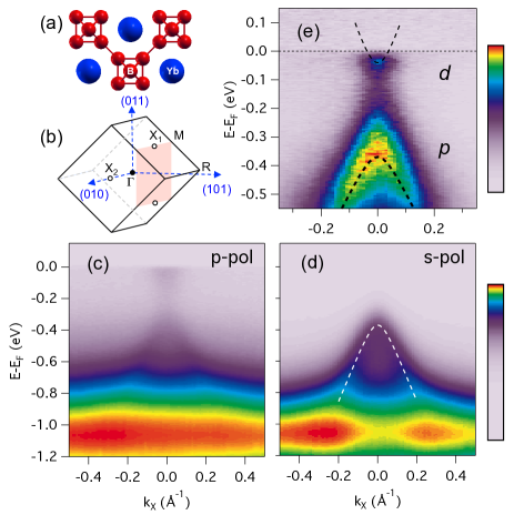
For insulating hexaborides, the polarity of (001) surfaces with different charge terminations can lead to - and -type band bending and quantum well states that make it difficult for ARPES to directly observe the bulk band gap. Also spectra from spatially inhomogeneous regions (i.e., both - and -type) can falsely appear to show Dirac cones or - overlap Frantzeskakis14 ; Denlinger15 . While surface modification and aging provide some control over the band bending and assist in the ARPES interpretations Denlinger15 , these problematic band-bending effects can be avoided by instead measuring a non-polar surface such as the (110) surface whose charge neutral bulk-termination is schematically illustrated in Fig. 1(a). For this purpose, a (110) surface of YbB6 was prepared from the natural facet of a single crystal grown by the aluminum-flux method. After etching in hydrochloric acid and ion sputtering of the surface, the sample was annealed to 1300 ∘C in ultra high vacuum to produce a spatially uniform 1 1 ordered surface suppl .
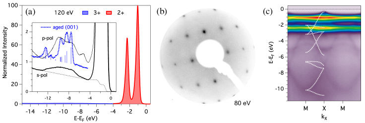
X-point ARPES spectra measured along M-X-M at = 120 eV using two different linear polarizations of the incident light is shown in Figs. 1(c) and (d). Above a strong Yb 4 peak at eV, the -polarization spectrum shows a weak hole-band dispersion and a small electron-like intensity at . A strong polarization selectivity of these states is revealed by the -polarization spectrum in Fig. 1(d), where the electron conduction state is totally suppressed and the valence hole band is strongly enhanced to manifest a triangular-like dispersion with a rounded-maximum and hybridization interaction with the Yb 4 states. The strong hole-band intensity allows a quantitative fit (dashed line) to a two-band non-parabolic dispersion model suppl with a band maximum of 0.35 eV below .
Figure 1(e) shows an enlarged view of the -polarization spectrum in which the Yb 4 spectral intensity tail has been divided out to obtain an enhanced image of the 0.3 eV semiconductor band gap between the B 2 valence and Yb 5 conduction states. To further characterize the conduction band dispersion and energy minimum, K-dosing of the surface was used to induce a small -type band bending until the electron pocket was increased in depth to 0.2 eV revealing enough of a dispersion suppl to perform similar non-parabolic dispersion analysis. The resulting process exhibited no discernible surface band gap narrowing, thus allowing evaluation of a band gap of 0.32 eV.
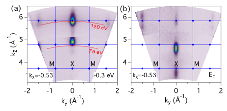
To explicitly confirm that the bands shown in Fig. 1 are bulk, we have measured their dependences in the process of locating the bulk X-points. Figures 2(a) and (b) show the - maps at fixed for the valence band at eV and the conduction band at , respectively. Both constant energy cuts exhibit strong intensity features close to bulk X-points at = 0 for = 76 eV and 120 eV as well as intensities at X-points of the second Brillouin zone (BZ) at . The small vertical -elongation of the X-point intensities in Fig. 2 is well accounted for by the inherent bulk band structure anisotropy (see Fig. 3) and the -broadening effect resulting from the finite inelastic mean free path of the photoelectrons. The pinning of at the bottom of the conduction band is consistent with the negative sign of the bulk Hall coefficient Tarascon80 ; Kim07 ; Zhou15 , and consistent with flat-band conditions of the non-polar (110) surface. Hence both the valence and conduction bands shown in Fig. 1 are 3D-like bulk bands and do not originate from the 2D-like surface states. The strong polarization dependence in Fig. 1(d) also independently confirms that these states are not linear Dirac cone dispersions, which would instead exhibit some continuity of the same orbital characters between the upper and lower parts of the Dirac cone.
The bulk X-point spectrum in Fig. 1(e) exhibiting a clear small direct semiconductor gap between valence and conduction band states and the absence of in-gap surface states is the central experimental result of this study. The (110) ARPES definitively proves the absence of a - overlapping band structure and hence a lack of parity inversion that is the key first requirement for a topological electronic structure interpretation of previous ARPES for the (001) surface. Therefore, the observed chirality in 2D surface states of YbB6 (001) in circular-dichroism (CD) Xia14 and spin-resolved ARPES Xu14 , cited to support the TI scenario of single-spin in-gap states, must have alternative explanations. Geometrical and final state effects are known to allow the detection of CD and spin-polarization in photoemission of non-chiral and non-magnetic solids Schohense90 ; sarpes , and can prevent an unambiguous detection of spin-polarization asymmetries in YbB6, as discussed elsewhere Denlinger15 .
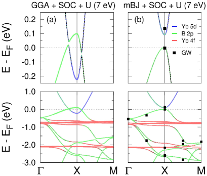
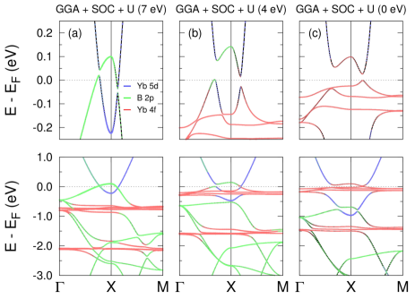
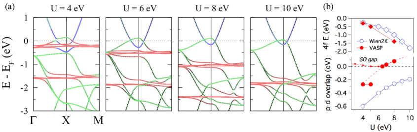
Next we turn our attention to theoretical predictions of the YbB6 electronic structure using the DFT method. We first reproduce the literature result Jun07 of a GGA + SOC + (7 eV) calculation for YbB6 in Fig. 3(a), which predicts a semimetallic band structure with a - band overlap at . The local gapping at the band crossing points arises from rather weak 5 SOC Cross . Since the - overlap anti-crossing points vary in energy around the X-point, the small local gapping cannot produce a full bulk gap, resulting in a complex semimetallic Fermi surface (FS), consisting of “lens” hole and “napkin ring” electron sheets. The calculated YbB6 4 BE of 0.7-0.8 eV relative to the valence band maximum is in agreement with the experimental ARPES result in Fig. 1 of 1.05 eV which includes the 0.32 eV band gap. The location of the 4 state far from results in only a minor influence on the semimetallic FS that is thus very similar to predictions of the non-rare-earth divalent hexaborides Massidda00 ; Hasegawa79 ; Rodriguez00 .
In Fig. 3(b), we present an mBJ + SOC + (7 eV) band result, overlaid with open-core pseudopotential single pass GW band result (dots) suppl . In both cases, the small - overlap of the GGA + SOC + calculation in Fig. 3(a) is transformed into a small 0.1 eV semiconductor gap with good quantitative agreement between the two methods suppl . This result clearly indicates that YbB6 is a topologically trivial small band-gap semiconductor. Not surprisingly, slab calculations for both the YbB6 (001) and (110) surfaces also show no topological in-gap surface states (see the Supplement suppl ).
This semiconductor result is reminiscent of the case of CaB6, whose early DFT-based semimetallic model for anomalous transport was revised to be that of a 1 eV semiconductor with the assistance of GW theory Tromp01 , and subsequently confirmed with ARPES Denlinger02 and other experiments using high-purity boron samples Cho04 ; Rhyee04 . This straightforward theoretical prediction for YbB6 of being a topologically trivial semiconductor is in contrast to two recent calculations that predict YbB6 to be a TI based on - band inversion Weng14 or - inversion Neupane15 ; Chang15 . The flaws in these previous band calculations, resulting in incorrect Yb 4 binding energies and mixed valency, are discussed in detail in the Supplement suppl , along with angle-integrated valence band spectra from the (110) surface that provide definitive proof of the pure Yb divalency in YbB6 suppl , and thus additionally rule out these erroneous theory calculations.
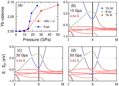
A recent pressure dependent study of YbB6 Zhou15 observes key results of (i) no structural transition up to 30 GPa from -ray diffraction, (ii) a rapid order-of-magnitude decrease in the resistivity up to 5 GPa, (iii) a pressure region of rather constant resistivity and Hall coefficient from 5 15 GPa, and (iv) a reemergence of thermally-activated resistivity above 15 GPa accompanied by a small increase in Yb valency from pure divalency to 2.09+.
The theoretical calculation at 15 GPa in Fig. 4(b) shows a - overlap band structure and indicates that YbB6 undergoes a semiconductor to semimetallic phase transition at an intermediate pressure. This occurs due to increase of and band widths and their wave function overlap. Such a - gap to - overlap transition naturally explains the rapid initial decrease in resistivity with pressure, also observed in early pressure-dependent transport of YbB6 Sidorov91 . A semimetallic state in the intermediate 5 15 GPa pressure regime is also suggested by the nearly constant Hall coefficient, which is attributable to a balance between electron and hole carriers Zhou15 . This transformation to semimetallic behavior under pressure provides a further confirmation of the existence of a semiconductor gap at ambient pressure where the ARPES experiments are performed.
The theoretical electronic structures for even greater pressures of 30 GPa and 50 GPa in Figs. 4(c) and (d) show an increasing - overlap such that the Yb 4 band ultimately touches the Yb 4 band which remains at nearly the same BE. The Yb 4 band exhibits only a small increase in bandwidth and slight centroid shift to lower BE but still remaining at the BE larger than 0.5 eV. Nevertheless there is an increased mixing of Yb 4 character into the -states, as evidenced by the increasing band anti-crossing gapping that results from the Yb 4 SOC interaction. The increasing Yb 4 character above implies a decreased -occupation and mixed-valency. Quantitative analysis of the Yb valence under pressure is plotted in Fig. 4(a). The resulting mixed-valence, less than 10% at the highest pressure, compares favorably to the experimental results derived from Yb -ray absorption measurements Zhou15 . The experimental reemergence of a thermally activated resistivity () above 15 GPa is plausibly due to the increasing 4 SOC-induced local gapping, whereas the overall resistivity rise due to gapping is weakened due to the competition of the increasing - overlap and hence increasing hole and electron FS volumes. The residual semimetallic conductivity can also explain the observed experimental low temperature resistivity plateaus Zhou15 .
This theoretical investigation allows us to comment generally on the feasibility of forming a TKI in actual materials. Since - states of opposite parity have inherently weak or negligible hybridization, the topologically non-trivial band inversion will have difficulty in forming a full insulator gap via hybridization alone. Therefore some additional external influence is required to open up an insulating gap of sufficient size to practically realize in-gap topological surface states. Here for the example of YbB6 under pressure, the external influence is the hybridization mixing of the Yb 4 states with the -states and its larger 4 SOC-induced gapping. However this effect is still too small for YbB6 to develop a full BZ - overlap gap at experimentally achievable pressures.
In conclusion, the flat-band conditions of the non-polar (110) surface allow ARPES measurements to definitively show that YbB6 is a non-Kondo non-TI semiconductor, and it opens up a new method for the quantitative characterization of the bulk gap of other divalent hexaborides. This result is in good agreement with predictions of theoretical DFT+ calculations with proper treatment of 4 correlations and inclusion of well-established gap correction physics. Only under pressure does the topologically non-trivial - band inversion occur, but the system still retains a semimetallic electronic structure even up to high pressure beyond the onset of small Yb mixed valency.
Acknowledgments - This work was supported by the Korean NRF (No.2011-0028736, No.2013R1A1A2006416, No.2014R1A1A2056546, 2015R1A2A1A15053564), Max-Plank POSTECH/KOREA Research Initiative (No. KR 2011-0031558), the KISTI supercomputing center (No. KSC-2015-C3-007), and the Deutsche Forschungsgemeinschaft via SFB 1170 (C06). Experiments were supported by the U.S. DOE at the Advanced Light Source (DE-AC02-05CH11231).
References
- (1) S. Raghu, X.-L. Qi, C. Honerkamp, and S.-C. Zhang, Phys. Rev. Lett. 100, 156401 (2008).
- (2) D. Pesin and L. Balents, Nat. Phys. 6, 376 (2010).
- (3) D. N. Sheng, Z.-C. Gu, K. Sun, and L. Sheng Nature Commun. 2, 389 (2011).
- (4) J. Maciejko and G. A. Fiete, Nat. Phys. 11, 385 (2015).
- (5) M. Dzero, K. Sun, V. Galitski, and P. Coleman, Phys. Rev. Lett. 104, 106408 (2010).
- (6) T. Takimoto, J. Phys. Soc. Jpn. 80, 123710 (2011).
- (7) M. Dzero, K. Sun, P. Coleman, and V. Galitski, Phys. Rev. B 85, 045130 (2012).
- (8) F. Lu, J.-Z. Zhao, H. Weng, Z. Fang, and X. Dai, Phys. Rev. Lett. 110, 096401 (2013).
- (9) S. Wolgast, Ç. Kurdak, K. Sun, J. W. Allen, D.-J. Kim, and Z. Fisk, Phys. Rev. B 88, 180405(R) (2013).
- (10) D. J. Kim, S. Thomas, T. Grant, J. Botimer, Z. Fisk, and J. Xia, Sci. Rep. 3, 3150 (2013).
- (11) D. J. Kim, J. Xia, and Z. Fisk, Nat. Mater. 13, 466 (2014).
- (12) J. D. Denlinger, J. W. Allen, J.-S. Kang, K. Sun, J.-W. Kim, J. H. Shim, B. I. Min, D.-J. Kim, and Z. Fisk, arXiv:1312.6637 (2013).
- (13) M. Neupane, N. Alidoust, S.-Y. Xu, T. Kondo, Y. Ishida, D. J. Kim, C. Liu, I. Belopolski, Y. J. Jo, T.-R. Chang, H.-T. Jeng, T. Durakiewicz, L. Balicas, H. Lin, A. Bansil, S. Shin, Z. Fisk, and M. Z. Hasan, Nature Commun. 4, 2991 (2013).
- (14) N. Xu, X. Shi, P. K. Biswas, C. E. Matt, R. S. Dhaka, Y. Huang, N. C. Plumb, M. Radović, J. H. Dil, E. Pomjakushina, K. Conder, A. Amato, Z. Salman, D. McK. Paul, J. Mesot, H. Ding, and M. Shi, Phys. Rev. B 88, 121102(R) (2013).
- (15) C.-H. Min, P. Lutz, S. Fiedler, B. Y. Kang, B. K. Cho, H.-D. Kim, H. Bentmann, and F. Reinert, Phys. Rev. Lett. 112, 226402 (2014).
- (16) M. M. Yee, Y. He, A. Soumyanarayanan, D.-J. Kim, Z. Fisk, and J. E. Hoffman, arXiv:1308.1085 (2013).
- (17) S. Rössler, T.-H. Jang, D. J. Kim, L. H. Tjeng, Z. Fisk, F. Steglich, and S. Wirth, Proc. Natl. Acad. Sci. (USA) 111, 4798 (2014).
- (18) B. Yan, L. Müchler, X.-L. Qi, S.-C. Zhang, and C. Felser, Phys. Rev. B 85, 165125 (2012).
- (19) X. Zhang, H. Zhang, J. Wang, C. Felser, and S.-C. Zhang, Science 335, 1464 (2012).
- (20) X. Deng, K. Haule, and G. Kotliar, Phys. Rev. Lett. 111, 176404 (2013).
- (21) Z. Li, J. Li, P. Blaha, and N. Kioussis, Phys. Rev. B 89, 121117(R) (2014).
- (22) H. Weng, J. Zhao, Z. Wang, Z. Fang, and X. Dai, Phys. Rev. Lett. 112, 016403 (2014).
- (23) C.-J. Kang, H. C. Choi, K. Kim, and B. I. Min, Phys. Rev. Lett. 114, 166404 (2015).
- (24) D. Kasinathan, K. Koepernik, L. H. Tjeng, and M. W. Haverkort, Phys. Rev. B 91, 195127 (2015).
- (25) A. Kakizaki, A. Harasawa, T. Kinoshita, T. Ishii, T. Nanba, and S. Kunii, Physica B 186-188, 80 (1993).
- (26) M. Xia, J. Jiang, Z. R. Ye, Y. H. Wang, Y. Zhang, S. D. Chen, X. H. Niu, D. F. Xu, F. Chen, X. H. Chen, B. P. Xie, T. Zhang, and D. L. Feng, Sci. Rep. 4, 5999 (2014).
- (27) M. Neupane, S.-Y. Xu, N. Alidoust, G. Bian, D. J. Kim, C. Liu, I. Belopolski, T.-R. Chang, H.-T. Jeng, T. Durakiewicz, H. Lin, A. Bansil, Z. Fisk, and M. Z. Hasan, Phys. Rev. Lett. 114, 016403 (2015).
- (28) N. Xu, C. E. Matt, E. Pomjakushina, J. H. Dil, G. Landolt, J.-Z. Ma, X. Shi, R. S. Dhaka, N. C. Plumb, M. Radović, V. N. Strocov, T. K. Kim, M. Hoesch, K. Conder, J. Mesot, H. Ding, and M. Shi, arXiv:1405.0165 (2014).
- (29) E. Frantzeskakis, N. de Jong, J. X. Zhang, X. Zhang, Z. Li, C. L. Liang, Y. Wang, A. Varykhalov, Y. K. Huang, and M. S. Golden, Phys. Rev. B 90, 235116 (2014).
- (30) T.-R. Chang, T. Das, P.-J. Chen, M. Neupane, S.-Y. Xu, M. Z. Hasan, H. Lin, H.-T. Jeng, and A. Bansil, Phys. Rev. B 91, 155151 (2015).
- (31) J. Jun, B. Jiang, and L. Lemin, Journal of Rare Earths 25, 654 (2007).
- (32) F. Tran and P. Blaha, Phys. Rev. Lett. 102, 226401 (2009).
- (33) Y. Zhou, D.-J. Kim, P. F. S. Rosa, Q. Wu, J. Guo, S. Zhang, Z. Wang, D. Kang, W. Yi, Y. Li, X. Li, J. Liu, P. Duan, M. Zi, X. Wei, Z. Jiang, Y. Huang, Y.-f. Yang, Z. Fisk, L. Sun, and Z. Zhao, Phys. Rev. B 92, 241118(R) (2015).
- (34) See Supplementary Material, which includes Refs. [35-46], for the detailed ARPES data and DFT results for YbB6, and the link between YbB6 and SmB6.
- (35) T. Nanba, M. Tomikawa, Y. Mori, N. Shino, S. Imada, S. Suga, S. Kimura, and S. Kunii, Physica B 186-188, 557 (1993).
- (36) J. L. Gavilano, Sh. Mushkolaj, D. Rau, H. R. Ott, A. Bianchi, and Z. Fisk, Physica B 329-333, 570 (2003).
- (37) E. O. Kane, J. Phys. Chem. Solids 1, 249 (1957).
- (38) J. A. Lo’pez-Villanueva, I. Melchor, P. Cartujo, and J. E. Carceller, Phys. Rev. B 48, 1626 (1993).
- (39) G. Kresse and J. Furthmüller, Phys. Rev. B 54, 11169 (1996); Comput. Mater. Sci. 6, 15 (1996).
- (40) G. K. H. Madsen and P. Novák, Europhys. Lett. 69, 777 (2005).
- (41) B. Lee and L.-W. Wang, Appl. Phys. Lett. 87, 262509 (2005).
- (42) Z.-H. Zhu, A. Nicolaou, G. Levy, N. P. Butch, P. Syers, X. F. Wang, J. Paglione, G. A. Sawatzky, I. S. Elfimov, and A. Damascelli, Phys. Rev. Lett. 111, 216402 (2013).
- (43) R. Monnier and B. Delley, Phys. Rev. B 70, 193403 (2004).
- (44) C.-J. Kang and B. I. Min, unpublished.
- (45) J. D. Denlinger, Sooyoung Jang, G. Li, L. Chen, B. J. Lawson, T. Asaba, C. Tinsman, F. Yu, K. Sun, J. W. Allen, C. Kurdak, D.-J. Kim, and Z. Fisk and Lu Li, arXiv:1601.07408 (2016).
- (46) P. Hlawenka, K. Siemensmeyer, E. Weschke, A. Varykhalov, J. Sanchez-Barriga, N. Y. Shitsevalova, A. V. Dukhnenko, V. B. Filipov, S. Gabani, K. Flachbart, O. Rader, and E. D. L. Rienks, arXiv:1502.01542 (2015).
- (47) P. Blaha, K. Schwarz, G. K. H. Madsen, D. Kvasnicka, and J. Luitz, WIEN2k, (Karlheinz Schwarz, Techn. Universitat Wien, Austria, 2001).
- (48) J. Kuneš and W. E. Pickett, Phys. Rev. B 69, 165111 (2004).
- (49) D. J. Singh, Phys. Rev. B 82, 205102 (2010).
- (50) J. D. Denlinger, APS March Meeting 2015, http://meetings.aps.org/link/BAPS.2015.MAR.J10.13
- (51) J. M. Tarascon, J. Etourneau, P. Dordor, P. Hagenmuller, M. Kasaya, and J. M. D. Coey, J. Appl. Phys. 51, 574 (1980).
- (52) J. Y. Kim, N. H. Sung, and B. K. Cho, J. Appl. Phys. 101, 09D512 (2007).
- (53) G. Schönhense, Physica Scripta T31, 255 (1990).
- (54) Spin-resolved ARPES controversies are discussed in I. Gierz , arXiv:1004.1573v2 (2011); C. Jozwiak , Nat. Phys. 9, 293 (2013); J. Sánchez-Barriga , Phys. Rev. X 4, 011046 (2014).
- (55) In the presence of SOC, both p-d bands have the same symmetries, e.g., along -X. But, without the SOC, they have different band symmetries, e.g., and , respectively, and so no local anticrossing gap opens along -X.
- (56) S. Massidda, R. Monnier, and E. Stoll, Eur. Phys. J. B 17, 645 (2000).
- (57) A. Hasegawa and A. Yanase, J. Phys. C: Solid State Phys. 12, 5431 (1979).
- (58) C. O. Rodriguez, R. Weht, and W. E. Pickett, Phys. Rev. Lett. 84, 3903 (2000); 86, 1142 (2001).
- (59) H. J. Tromp, P. van Gelderen, P. J. Kelly, G. Brocks, and P. A. Bobbert, Phys. Rev. Lett. 87, 016401 (2001).
- (60) J. D. Denlinger, J. A. Clack, J. W. Allen, G.-H. Gweon, D. M. Poirier, C. G. Olson, J. L. Sarrao, A. D. Bianchi, and Z. Fisk, Phys. Rev. Lett. 89, 157601 (2002).
- (61) B. K. Cho, J.-S. Rhyee, B. H. Oh, M. H. Jung, H. C. Kim, Y. K. Yoon, J. H. Kim, and T. Ekino, Phys. Rev. B 69, 113202 (2004).
- (62) J.-S. Rhyee and B. K. Cho, J. Appl. Phys. 95, 6675 (2004).
- (63) V. A. Sidorov, N. N. Stepanov, O. B. Tsiok, L. G. Khvostantsev, I. A. Smirnov, and M. M. Korsukova, Sov. Phys. Solid State 33, 720-723 (1991).
Supplemental Material:
Electronic structure of YbB6 : is it a Topological Insulator or not?
I ARPES of non-polar (110) surface
I.1 A. Yb divalency and wide EDC
The deep binding energy (BE) of the bulk Yb 4f levels and lack of Yb2+ spectral weight near the Fermi level is strong experimental evidence for pure divalency in YbB6. However, another important test for mixed-valency is the observation and quantification of the relative amount of Yb3+ spectral weight in valence band photoemission measurements. Previous XPS and UPS measurements sm-Kakizaki93 ; sm-Nanba93 observed distinct Yb3+ contributions to Yb 4p core-level and valence band spectra, but the origin was ascribed to surface contributions. Similarly, a weak ferromagnetic moment corresponding to 2% bulk trivalency was initially reported in YbB6 sm-Gavilano03 . But later measurements showed stoichiometric YbB6 to be diamagnetic, with surface ferromagnetism or paramagnetism appearing only for non-stoichiometric samples sm-Kim07 .
In Fig. S1(a), we demonstrate the pure divalency of Yb from a wide valence band spectrum for a prepared YbB6 (110) surface measured at = 120 eV. The spectrum exhibits Yb2+ and peaks that dominate over the very weak 4 - 12 eV BE range where Yb3+ spectral weight would be found. Overlapping in this energy range are B-sp valence band states whose relative cross section is low at this photon energy and which can be further suppressed using s-polarization of the incident photons, as shown in the Fig. S1(a) inset.
The line shape of the valence band structure, shown in the expanded view of this 4 12 eV range, exhibits no evidence for any Yb3+ spectral weight whose distinct final state multiplet peak structure is illustrated in the inset of Fig. S1(a) (dashed line). This example of a Yb3+ spectrum comes from a cleaved (001) surface that initially looks like the pure divalent (110) surface spectra, but then develops within only 4 hours the appearance of this Yb3+ signature, indicating the trivalent conversion of surface Yb atoms due to residual gas adsorption. In contrast, the (110) surface with coplanar Yb and B6 termination and 1 1 surface order, shown in Fig. S1(b), exhibits no spectral changes after greater than 12 hours of measurement. Even if one integrates the B-sp spectral weight of the s-polarization spectrum, after employing the background subtraction shown in Fig. S1(a), and assigns it to Yb3+, one obtains an upper bound contribution of less than 1%. This tight experimental upper bound on the pure divalency of Yb in YbB6 immediately rules out both of the theoretical predictions of - sm-Weng14 and - sm-Neupane15 ; sm-Chang15 band inversion scenarios, both of which predict mixed Yb valency.
A 12 eV wide angle-resolved spectrum measured at the 120 eV bulk X-point, shown in Fig. S1(c), also illustrates the wide B-sp band dispersions in the 4 - 12 eV range, and the absence of any -independent Yb3+ peaks. The spectrum additionally illustrates the 1 eV and 2.3 eV binding energies of the Yb and Yb states, respectively. The Yb 4 peaks are observed to be uniform across the prepared (110) sample surface, in contrast to the reported energy shifts between cleaves, and spatial inhomogeneity of the cleaved (001) surface sm-Xia14 ; sm-Xu14 ; sm-Frantzeskakis14 . The boron hole band that forms the valence band maximum is observed to disperse from below the Yb state and significantly hybridize with the f-states as it passes through towards . A small band width expansion of 1.05 of the DFT bands was required to best match experiment.
I.2 B. X-point location
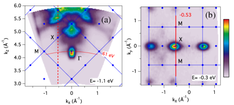
A suitable bulk X-point location for the band gap determination was chosen based on photon-dependent and angular-dependent mapping of the momentum-space. First a normal-emission photon-dependent map was acquired with the sample axis aligned vertically with the spectrometer slit. An energy cut at eV, between the two 4f states, highlights a strong feature at 61 eV, as shown in Fig. S2(a) that aligns to the bulk Brillouin zone (BZ) using an inner potential parameter of 14 eV.
Then the sample is rotated in azimuth to align the sample (100) axis to the vertical spectrometer slit and an off-normal photon-dependent map was acquired at fixed as indicated in Fig. S2(a). The map at fixed , presented in Fig. 2(a) of the main text, with an energy cut 0.3 eV below probing the valence band hole dispersion, shows two strong hole-band features at = 0 for = 76 eV and 120 eV as well as at four weaker intensity second BZ X-points at .
= 120 eV was chosen for the angular-dependent map in Fig. S2(b) with the same sample orientation. Similar to the photon-dependent map, strong valence band hole intensities are observed at three different X-points at = 0 and also additionally at four more X-points in the second BZ at . The bulk X-point at was used for Fig. 1(e) in the main text and was checked for consistency at other bulk X-points.
I.3 C. K-dose
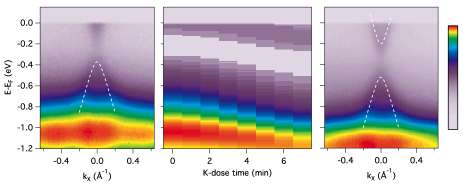
To further characterize the conduction band minimum energy, surface K-dosing was used to create a small -type band bending until the electron pocket was sufficiently deep to observe its non-parabolic dispersion. For this experiment, an X-point spectrum was obtained at 76 eV instead of 120 eV due to the strong -electron (-hole) band intensity for () polarization, allowing a good quantitative analysis of the non-parabolic conduction (valence) band dispersion and semiconductor gap evaluation (see subsection D).
Fig. S3(a) shows the X-point -polarization spectrum before K-dosing. Fig. S3(b) shows a time/dosing dependent energy distribution curve (EDC) cut at X illustrating the energy shifts of the valence and conduction bands as well as the Yb 4f state. The final EDC spectrum, shown in Fig. S3(c), is a sum of - and -polarizations due to the weakening of the p-hole band with K-dosing. Because a rigid shift of both valence and conduction bands is observed in Fig. S3(b) with no discernible surface band gap narrowing, we can claim that this K-dosed analysis is reflective of a bulk gap of magnitude 0.32 eV, based on non-parabolic dispersion visual fits to the polarization-dependent data that best highlight either the hole valence band or electron conduction band dispersions sm-Denlinger15 .
I.4 D. Non-parabolic Dispersion
A two-band model for non-parabolic valence and conduction bands in the presence of small band gaps sm-Kane57 was used to assist in the determination of the valence band maximum and conduction band minimum energies. The two band correction to the free electron parabolic dispersion can be written simply as sm-Lopez93 :
| (1) |
where and are the energy gap parameter and the electron effective mass, respectively.
The energy gap dependence of Eq. (1) exhibits the well-known progression towards a purely linear V-shaped dispersion at zero gap, corresponding to a Dirac semimetal. The valence band dispersion in Fig. 1(d) of the main text exhibits linearity away from a distinctly rounded band maximum and is nicely fit using the nominal experimental gap value of 0.3 eV and an effective mass of = 0.12. This dispersion shape for intermediate small gap values contrasts sharply with topological Dirac cone surface states in Bi2X3 (X = Se, Te), where the dispersion is mostly linear near the Dirac point and deviates further away (e.g., hexagonal warping).
The conduction band dispersion, revealed after K-dosing in Fig. S3(c), is similarly fit to = 0.3 eV and = 0.1.
II Computational details
The band calculations were performed by using the full-potential linearized augmented plane-wave (FLAPW) band method, as implemented in the WIEN2K package sm-wien2k . For the DFT calculations, the PBE (Perdew-Burke-Ernzerhof) exchange-correlation functional was used in the GGA (generalized-gradient approximation). The spin-orbit coupling (SOC) was included in a way of the second variational method. In the GGA + SOC + method, a correlation energy of eV was chosen to obtain the correct experimental value of the Yb 4f BE of 1 eV, which is consistent with the previous calculations sm-Jun07 ; sm-Kunes04 . The mBJ potential corresponds to an orbital-independent semilocal exchange potential that mimics the behavior of orbital-dependent potentials and has been shown to provide band gap corrections in good agreement with the improved many-body but more computation-demanding GW calculation sm-TB09 ; sm-Singh10 . A single pass open-core pseudopotential GW calculation was also performed using VASP sm-vasp , which effectively removes the Yb 4f levels from the calculation. This is reasonable in view of the deep 4f BE in YbB6.
In the GGA + (: on-site Coulomb interaction of Yb electrons) calculations, the scheme of a fully-localized limit was used for the 4f electrons. The BZ integration was done with a 17 17 17 -mesh, and, in the FLAPW calculations, muffin-tin radii ’s of Yb and B were chosen to be 2.50 and 1.59 a.u., respectively, and the plane-wave cutoff was = 7.
For the GW calculation, a single pass open-core pseudopotential G0W0 calculation was performed using VASP with a 4 4 4 -mesh, 400 unoccupied bands and 80 mesh size in the omega frequency.
YbB6 crystallizes in the CsCl-type structure, like SmB6. The ambient pressure calculations were performed using the experimental YbB6 lattice parameter of a = 4.1792 Å and internal crystal parameter = 0.202 that specifies the relative inter-octahedron B-B bond length sm-Jun07 . For pressure-dependent calculations, a linear relation between the lattice constant and applied pressure up to 30 GPa was established using -ray diffraction data in Ref. sm-Zhou15 , before starting the relaxation. To obtain the structure information under 50 GPa, where the lattice constant was not accessible in Ref. sm-Zhou15 , the fully relaxed calculation was performed. All electronic structure calculations under pressure were done using the mBJ + SOC + (7 eV) scheme. We have checked the pressure dependent value by a constrained LDA calculation sm-Madsen05 and found that 7 eV is obtained over the whole pressure range, which could be interpreted as showing the strong localization of the Yb orbital.
III DFT + SOC + band structures for YbB6 with varying
Two recent calculations predict YbB6 to be a topological insulator (TI) based on - band inversion sm-Weng14 or - inversion sm-Neupane15 ; sm-Chang15 . The first was an LDA + Gutzwiller calculation with = 6 eV that erroneously predicted a topological - inverted band structure very similar to SmB6 sm-Lu13 , with a highly incorrect 4 BE of 0.1 eV. The LDA + Gutzwiller result sm-Weng14 is empirically very similar to a = 0 DFT result in Fig. S4(c) in terms of the 4 BE and the - band inversion at .
A second proposed topological band structure for YbB6, based on DFT + pseudopotential VASP calculations using small values of 4 eV sm-Neupane15 or 5 eV sm-Chang15 , obtains a - band overlap but with a small insulating gap throughout the bulk BZ, similar to that in Fig. S4(b) sm-Replica . The effect of the smaller values is a smaller Yb 4 BE, 0.3 (0.5) eV for = 4 (5) eV, whose closer proximity to the - overlap region at results in significant hybridization of the Yb 4 and B 2 states. This allows the Yb 4 SOC to open a larger - gap that otherwise is intrinsically tiny due to the smallness of the 5 SOC. The hybridization of Yb 4 states into the - overlap region also results in a mixed-valent Yb 4-occupation evaluated to be 13.8, which does not agree with the experimental divalent state of Yb. Chang et al. sm-Chang15 also reported that the SOC-induced gapping of the - overlap at = 4 5 eV evolves into a topologically trivial - gap above = 6.5 eV. This result is in contradiction to the earlier literature result sm-Jun07 and our Wien2k result shown in Fig. S4(a). As shown in Fig. S5, the DFT + calculations for increasing yield only a small gradual decrease in the - overlap energy without opening up a semiconducting - gap even for unphysically large values as high as 15 eV. This is consistent with a decreasing influence of the Yb 4 states on the - states as they are pushed farther away from . Namely, large is not the formative parameter for the semiconductor gap.
One might consider that the 6.5 eV VASP prediction of a topologically trivial semiconductor is in agreement with the Wien2k mBJ + SOC + semiconductor result in Fig. 3(b) of main text. However this is entirely fortuitous because the VASP calculation does not contain the band gap renormalization treatment of the mBJ or GW calculations in Fig. 3(b). Chang et al. sm-Chang15 also presented a GW calculation for YbB6 but for = 0 with the goal of demonstrating that GW alone cannot produced the - band inversion. In contrast, the VASP GW calculation in Fig. 3(b) is an open-core calculation, which simulates a large effective that removes the Yb 4 states far from . Thus the GW calculation in Fig. 3(b) treats the and correlations that renormalize the - overlap into a small semiconductor gap.
We have also checked DFT + electronic structures using VASP. The crystal structure was fully relaxed using the GGA + SOC scheme ( = 4.13 Å, = 0.201). The resultant crystal structure was quite similar to the experimental structure. Band structures of YbB6 were calculated with various values in both relaxed and experimental structures, and it was found that the band structures for the two cases are almost the same. We have found that our VASP results are quite consistent with our Wien2k results. There is a sensitivity of the - overlap to the internal structural parameter sm-Lee05 . One could speculate that differences in structural input could be a possible source of the discrepancy between our Wien2k (and VASP) and the published VASP calculations sm-Neupane15 ; sm-Chang15 , but no structural information (lattice constant or ) was provided in Refs. sm-Neupane15 ; sm-Chang15 .
Figure S5(b) shows the comparison between the VASP results by Chang et al. sm-Chang15 vs. our Wien2k results, which highlights the discrepancy for 6 eV. We can note discrepancies between two in (i) the binding energy of Yb 4 band () and (ii) - overlap. The VASP results of the latter by Chang et al. look merely shifted Wien2k results.
In summary, we note that the incorrect - overlap sm-Weng14 , and - overlap sm-Neupane15 ; sm-Chang15 calculations did not cite the earlier Wien2k calculation of Ref. sm-Jun07 , and hence failed to compare and discuss their discrepancies with the published literature. We also note that the complicated intermixing of all three , and states near with interplay of 4 SOC and mixed valency discussed in the main text for the high-pressure phase of YbB6 is the same physics at the heart of the erroneous claim of a TI - overlap gap at ambient pressure sm-Neupane15 ; sm-Chang15 , albeit errantly realized from a too small value of .
A remaining open question about the ambient pressure phase is the quantitative disagreement between the experimental 0.3 eV and theoretical 0.1 eV gaps, which would be worthwhile to be investigated theoretically. Further theoretical investigation of the high pressure phase is warranted to address whether any low energy scale dynamical correlations (e.g. Kondo effect) can emerge from the small mixed valency, or whether any non-trivial topological - parity inversion effects can be realized while in a partially gapped semimetallic state.
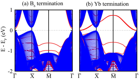
IV DFT slab calculation for YbB6 (001) surface
In order to examine the surface states, we have also carried out DFT open-core slab calculations for the YbB6 (001) surface using VASP. We have used slab structures composed of 9 Yb and 8 B6 layers for Yb termination and 8 Yb and 9 B6 layers for B6 termination, and for both terminations, 30 Å vacuum layers were considered. We have first relaxed the slab structures for both terminations, and then self-consistent calculations were performed with a 10 10 1 -mesh. For the purpose of getting a topologically trivial - bulk gap in the DFT + SOC + (7 eV) without employing mBJ, we employed an increased lattice constant of in the slab calculations.
As shown in Fig. S6, surface states (red lines) appear for both B6 and Yb terminations. These surface states, however, are just topologically trivial surface states, which are often observed in the hexaboride systems sm-Zhu13 ; sm-Monnier04 . The Dirac-cone-like surface states observed in ARPES are not obtained. In fact, such Dirac cones are expected to be quantum well states coming from the band bendings in the polar (001) surfaces with different charge terminations sm-Frantzeskakis14 ; sm-Denlinger15 .
The DFT open-core slab calculations for the non-polar (110) surface also produce similar surface states, one deep surface band of B character and two surface bands near of mixed B and Yb characters that arise from broken bond states from surface B atoms sm-CJKang15 . All of those surface states are topologically trivial.
V Link between YbB6 and SmB6
There are strong differences in issues of the two materials YbB6 and SmB6 i.e., pure-divalency and - overlap/semiconductor gap issues in YbB6 and mixed valency and - hybridization gap issues in SmB6. Also note that while YbB6 (001) ARPES shows “false” in-gap states that are actually band-bending quantum well states, the YbB6 (110) ARPES show no states within the 0.3 eV semiconductor gap, thereby disproving the TI scenario for YbB6.
In contrast for SmB6 the 20 meV hybridization gap exhibits similar ARPES in-gap states for both the polar (001) and non-polar (110) surfaces sm-Denlinger16 . The existence of the X-point in-gap states for SmB6 is insensitive to the different polar surface terminations, and similar in-gap states are observed for the non-polar (110) surface too sm-Denlinger16 . Hence the polar nature alone cannot explain the in-gap states, although polar effects are still being discussed for the (001) surface, e.g., in the context of 2D-like -states outside the gap sm-Hlawenka15 .
We have also checked the mBJ scheme for SmB6. The reason why we used the mBJ scheme for YbB6 is to consider the correlation effects of delocalized Yb 5 and B 2 electrons near . While it is very crucial for YbB6 that the mBJ correction changes the - overlap into a - trivial gap, for SmB6, the Sm 4 bands are dominating near , and so the mBJ method does not play a crucial role. In fact, we have confirmed for SmB6 that the DFT and mBJ results are essentially the same sm-CJKang15 .
For SmB6, dynamical mean-field theory (DMFT) is essential to address the dynamic energy correlations that result in strong low energy scale renormalization of the -states near as well as the mixed valency. In contrast, for YbB6, with the large binding energy of the 4 states and pure divalency, one would not expect any low energy scale dynamical correlations to emerge from DMFT calculations. Indeed we have checked and confirmed for YbB6 that DFT + DMFT gives essentially identical results as DFT + , i.e., a proper 4 binding energy and an uncorrected - overlap sm-CJKang15 . The latter is because the correlation effects of delocalized and electrons are not treated within DMFT.
References
- (1) A. Kakizaki , Physica B 186-188, 80 (1993).
- (2) T. Nanba , Physica B 186-188, 557 (1993).
- (3) J. L. Gavilano , Physica B 329-333, 570 (2003).
- (4) J. Y. Kim, N. H. Sung, and B. K. Cho, J. Appl. Phys. 101, 09D512 (2007).
- (5) H. Weng , Phys. Rev. Lett. 112, 016403 (2014).
- (6) M. Neupane , Phys. Rev. Lett. 114, 016403 (2015).
- (7) T.-R. Chang , Phys. Rev. B 91, 155151 (2015).
- (8) M. Xia , Sci. Rep. 4, 5999 (2014).
- (9) N. Xu , arXiv:1405.0165 (2014).
- (10) E. Frantzeskakis , Phys. Rev. B 90, 235116 (2014).
- (11) J. D. Denlinger, APS March Meeting 2015, http://meetings.aps.org/link/BAPS.2015.MAR.J10.13
- (12) E. O. Kane, J. Phys. Chem. Solids 1, 249 (1957).
- (13) J. A. Lo’pez-Villanueva, I. Melchor, P. Cartujo, and J. E. Carceller, Phys. Rev. B 48, 1626 (1993).
- (14) P. Blaha, K. Schwarz, G. K. H. Madsen, D. Kvasnicka, and J. Luitz, WIEN2k, (Karlheinz Schwarz, Techn. Universitat Wien, Austria, 2001).
- (15) J. Jun, B. Jiang, and L. Lemin, Journal of Rare Earths 25, 654 (2007).
- (16) J. Kuneš and W. E. Pickett, Phys. Rev. B 69, 165111 (2004).
- (17) F. Tran and P. Blaha, Phys. Rev. Lett. 102, 226401 (2009).
- (18) D. J. Singh, Phys. Rev. B 82, 205102 (2010).
- (19) G. Kresse and J. Furthmüller, Phys. Rev. B 54, 11169 (1996); Comput. Mater. Sci. 6, 15 (1996).
- (20) Y. Zhou , Phys. Rev. B 92, 241118(R) (2015).
- (21) G. K. H. Madsen and P. Novák, Europhys. Lett. 69, 777 (2005).
- (22) F. Lu, J.-Z. Zhao, H. Weng, Z. Fang, and X. Dai, Phys. Rev. Lett. 110, 096401 (2013).
- (23) The Wien2k = 4 eV calculation in Fig. S4(b) shows Yb 5 band below the states in contradiction to the Neupane et al.’s VASP = 4 eV calculation Neupane15 that shows the -band bottom above the states.
- (24) B. Lee and L.-W. Wang, Appl. Phys. Lett. 87, 262509 (2005).
- (25) Z.-H. Zhu , Phys. Rev. Lett. 111, 216402 (2013).
- (26) R. Monnier and B. Delley, Phys. Rev. B 70, 193403 (2004).
- (27) C.-J. Kang and B. I. Min, unpublished.
- (28) J. D. Denlinger , arXiv:1601.07408 (2016).
- (29) P. Hlawenka , arXiv:1502.01542 (2015).