Charging graphene nanoribbon quantum dots
Abstract
We describe charging a quantum dot induced electrostatically within a semiconducting graphene nanoribbon by electrons or holes. The applied model is based on a tight-binding approach with the electron-electron interaction introduced by a mean field local spin density approximation. The numerical approach accounts for the charge of all the electrons and screening of external potentials by states near the charge neutrality point. Both a homogenous ribbon and a graphene flake embedded within the ribbon are discussed. The formation of transport gaps as functions of the external confinement potential (top gate potential) and the Fermi energy (back gate potential) are described in good qualitative agreement with the experimental data. For a fixed number of excess electrons we find that the excess charge added to the system is, - depending on the voltages defining the work point of the device: i) delocalized outside the quantum dot – in the transport gap due to the top gate potential ii) localized inside the quantum dot – in the transport gap due to the back gate potential or iii) extended over both the quantum dot area and the ribbon connections – outside the transport gaps. The applicability of the frozen valence band approximation to describe charging the quantum dot by excess electrons is also discussed.
I Introduction
The dispersion relation of graphene Neto2009 – gapless and linear near the charge neutrality point – prevents electrostatic confinement of charge carriers Klein29 ; Young . The energy gap in the band structure is opened for finite strips of graphene nrb ; waka ; nrbr ; nrb4 which allows for carrier confinement by external potentials defining quantum dots inside the nanoribbons silvestrov07 ; han ; nrb3 ; trau ; oostinga ; xliu ; stampfer ; moreview ; droescher . All nanoribbons exhibit a transport gap han ; nrb2 near the neutrality point. Formation of the transport gap can be described theoretically already for non-interacting electrons as due to lateral confinement and edge disorder evaldsson . Nevertheless, the Anderson localization effects are reinforced by the electron-electron interaction and according to the present understanding, the transport gap is stabilized by a spontaneous formation of multiple Coulomb islands along the ribbon. The current peaks that appear for a biased ribbon inside the transport gap are attributed to electrons hopping between the charge puddles sols ; stampfer ; xliu ; nrb3 ; chiu ; mhan ; todd ; gala . Charging of the intentionally defined quantum dots appears also within the transport gap chiu ; stampfer ; moreview ; droescher . The spontaneous disorder-induced quantum dots and the ones defined electrostatically are characterized by Coulomb diamonds in the charge stability diagrams chiu ; stampfer ; xliu . In part of the studies the nanoribbons contain an additional inline graphene flake stampfer ; moreview ; gut ; chiu ; sch ; gutti in the gated region, which is useful in separationchiu of the charging effects due to the intentionally introduced quantum dot and the spontaneous Coulomb islands along the ribbon.
The electronic properties of quantum dots made of finite graphene flakes have been extensively studied in a number of papers Ezawa ; Potasz1 ; Yamamoto ; Zhang ; Guclu ; Potasz2 ; Palacios ; Wang ; Zarenia ; Wunsch and only recently a finite graphene flake was successfully connected directly to source-drain electrodes without nanoribbons feeding the charge to the flake mori . Localization of electrons within a quantum dot induced electrostatically inside a graphene sheet with the mass gap induced by the substrate have been studied in Ref. rontani, , and the one-electron properties of these dots were discussed in Refs. these1, ; these2, .
The purpose of the present paper is a simulation of charging a quantum dot defined by an external potential within a graphene nanoribbon. We consider both homogenous ribbons and the ones containing an inline flake of graphene. We prepared a numerical model that covers formation of both n-type and p-type quantum dots confining conduction band electrons or valence bands holes depending on the sign of the external potential. For the purpose of the present study we consider a semiconducting armchair nanoribbon using the tight-binding approach for the single-electron spectrum and the LSDA potentials describing the electron-electron interaction. The model accounts for contribution of all the electrons within the sample in formation of the potential profile along the system. We find that within the transport gap the quantum dot charging in terms of the chemical potentials can be very well described in a single-electron basis limited to an energy range near the neutrality point. The charge density of the states deep inside the valence band can then be considered frozen without any detectable deviation from the electron-hole symmetry in terms of electron and hole charging processes. We discuss the transport gap and the charge distribution within the entire system including an integer quantization of the quantum-dot-confined charge. For a neutral system the modification of the lateral confinement - with introduction of the flake into the ribbon – does not induce formation of a localized charge puddle. Nevertheless, the excess electrons – when present within the system – get localized within the flake already in the absence of the external potential. A good qualitative correspondence with the transport gaps observed in Ref. xliu as functions of the back gate and the top gate potentials is found. Applicability of the approximation of a frozen valence band for charging the dot with excess electrons is also discussed.
a) 
|
b) 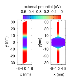
|
II Theory
We consider a finite ribbon with armchair edges [see Fig. 1(a)] with or without a hexagonal flake defined in its center. We use the single-electron Hamiltonian as given by the tight-binding method for orbitals
| (1) |
where eV is the hopping parameter, and is the operator of electron creation at -th atom and the summation runs over nearest neighbor atoms.
Upon diagonalization of the Hamiltonian we obtain the eigenstates of form
| (2) |
We assume 18 or 36 atoms across the ribbon, so that the system – in the tight-binding approach has a semiconducting dispersion relation [see Fig. 1]. The charge redistribution that we describe requires application of large external potentials, for which the potential at the ions is far from the charge neutrality point and the linear dispersion relation of graphene. For this reason we need to employ an atomistic tight-binding approach instead of its continuous low-energy approximation in the Dirac form. The atomistic approach has its price on computational complexity and memory consumption, that limits the size of the systems than can be studied. Nevertheless, the obtained picture is qualitatively independent of the size the systems and the ones considered in this work remain within an experimental reach. For applications of the graphene nanoribbons in electronics their width below 10 nm is needed to switch off the current cyt1 ; cyt2 . The external potential well defining the size of the quantum dot is 15-20 nm [Fig. 1(b)], while the estimated diameter of the quantum dot in a gated system is 25-40 nm mori .
The system of interacting electrons is treated by a mean field approach. The number of ions in the considered systems and the number of orbitals in the basis ranges up to about thousands, which sets the size of the basis (2). The considered systems are close to the charge neutrality, with the number of electrons within the ribbon close to the number of positive ions (net charge ). We have found that the ground-state properties of the system can be quite accurately described using a basis of a few hundred wave functions of type (2) for the energies near the neutrality point.
We order the single-electron basis functions by the energy eigenvalues , where is an integer non-zero index ( is an even number). For the LSDA Perdew calculations we use a basis of form
| (3) |
where is the spin index. The basis (3) contains single-electron states of both the valence (negative ) and the conduction bands (positive index). The states that are deep below the energy gap with are considered frozen. Their contribution to the electron spin density is calculated once and for all after diagonalization of the single-electron Hamiltonian
| (4) |
For the simulation of the mean-field potential we neglect the overlap of neighbor orbitals; the approach is equivalent to two-center treatment of the Coulomb integrals 2center . Accordingly, the contribution of the th orbital to the spin density at -th ion is given by , and
| (5) |
The electron-electron interaction is introduced by the LSDA mean field potential Perdew , with the Hamiltonian of form
| (6) |
where is the electron creation operator in the eigenstate of Hamiltonian (1) with spin . The DFT potential enters the hopping parameters (),
| (7) |
where is the spin density
| (8) |
In the above formula is the spin density of electrons occupying energy levels close to the neutrality point which are determined by DFT,
| (9) |
where is the Fermi-Dirac distribution for the Fermi energy , and are the eigenvalues of the DFT energy operator (6). The Fermi energy is found from the normalization for the electron density ,
| (10) |
where is the number of electrons within the system , with that stands for the number of ions within the nanoribbon, and for the number of excess electrons with respect to a charge neutral system.
The potential defining the hopping parameters (7) is given by
| (11) |
The external electrostatic potential in Eq. (11) defining the quantum dot in the center of the ribbon is modelled by
| (12) |
where nm is the length of the quantum dot – see Fig. 1(b) for the profile plotted for eV. The electrostatic potential defining the quantum dot is assumed with an axial symmetry, since the gates are usually applied perpendicular to the nanoribbon xliu . The potential as induced electrostatically is smooth and - due to the screening- short range. The exact profile of the confinement potential depends on the size of the gates and their distance to the area occupied by electrons bednarek1 ; bednarek2 . The qualitative features for the charging of the quantum dots remain independent of the potential profile, as long as it is smooth and short range. The results for a modified form of the potential is given in Section IV.E, with power of 2 instead of 4 in Eq.(12).
The Hartree potential , is evaluated as
| (13) |
where the summation runs over the ions , and . We use the dielectric constant as for the graphene grown on SiC sicc .
In Eq. (11) is the potential of the carbon ions which is calculated in a similar manner
| (14) |
The exchange and correlation potentials are taken according to the Perdew-Zunger parametrization Perdew for the spin density given at the ions. Once, the potential are known, we calculate the hopping elements (7)
| (15) |
where
We evaluate the chemical potential of the electron system
| (16) |
where is the total energy, calculated as
| (17) |
with the kinetic energy
| (18) |
which can be expressed using the single-electron energy eigenvalues for operator (1) with eigenfunctions (3)
| (19) |
in Eq. (17) is the contribution to the energy of the external potential and the carbon lattice
| (20) |
in Eq. (17) is the Perdew-Zunger Perdew exchange-correlation energy and the last term of (17) is the Hartree energy
| (21) |
In the summation of the single-electron contributions to the kinetic energy (18) we account only for the orbitals forming the basis for the DFT calculation, since the contributions of lower energy levels – considered frozen – cancel in the evaluation of the chemical potential anyway. However, in the exchange-correlation and Hartree potential, the total electron density, including the frozen orbitals needs to be taken into account. For convergence of the DFT equations we use the Broydenbroyden method. The convergence is further additionally enhanced by annealing of the temperature. We start from 20K and take down the temperature to K. This range of the temperature corresponds to the one actually used in the experimental studies of graphene quantum dot todd . In the model system, which is small, below 10 K no further potential dependence on the temperature is observed.
| a) | 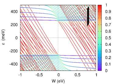 |
|---|---|
| b) | 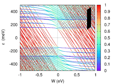 |
| c) | 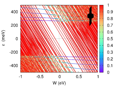 |
III Results and Discussion
III.1 Single-electron spectra
Let us first characterize the single-electron spectrum in the absence of the electron-electron interaction for the quantum dots induced within the ribbon. The energy spectrum is displayed in Fig. 2 as a function of the quantum dot potential for a nanoribbon of length nm and 18 or 36 atoms across the ribbon – Fig. 2(a) and (b), respectively. The colors of the plotted energy levels indicate the localization of the corresponding states. The red energy levels are entirely localized within the quantum dot area . For the quantum dot induced by the external potential in the homogenous ribbon the localized energy levels appear for . The dot-localized (red) energy levels for correspond to localized states of the conduction band (n-type quantum dot) and for to the localized states of the valence band (p-type quantum dot). The energy levels plotted in blue in Fig. 2 are localized entirely outside the quantum dot, generally near the ends of the ribbon, and they are insensitive to the dot potential.
At the charge neutrality point () [Fig. 2(a,b)] one observes an energy gap between the dot-localized (red) energy levels as a function of the dot potential . For we find localized conductance (valence) band states appearing for increasing (decreasing ). A gap is also observed as a function of the energy for a fixed . In the experimental conditions the transport gap is observed as a function of both the dot potential (top gate potential) and the Fermi energy (back gate potential) xliu . The latter corresponds to variation of the energy for a fixed value.
Figure 2(c) shows the spectra for the hexagonal flake embedded inside the ribbon with 18 atoms across the channel. For the flake the number of localized (red) energy levels [Fig. 2(c)] within the gap is much larger as compared to the nanoribbon quantum dot [cf. Fig. 2(a)], and the localized energy levels appear already at .
| a) |
 b)
b) |
 |
| c) |
 d)
d) |
 |
| e) |
 f)
f) |
 |
| g) |
 h)
h) |
 |

a) 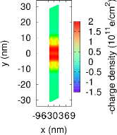 b)
b) 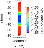 c)
c) 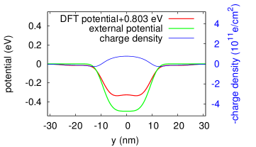
|
d) 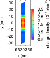 e)
e) 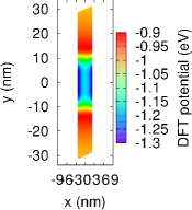 f)
f) 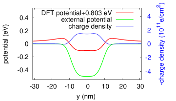
|
g) 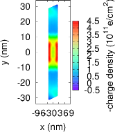 h)
h) 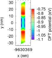 i)
i) 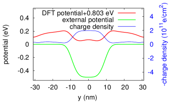
|
| a) | 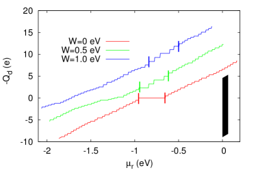 |
|---|---|
| b) | 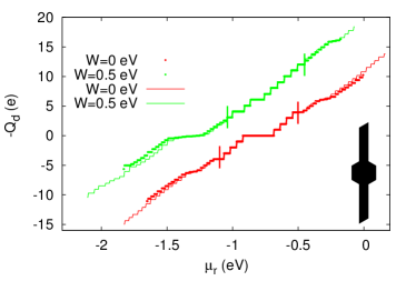 |
a) 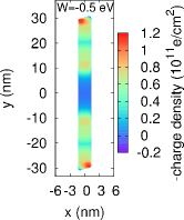
|
b) 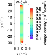
|
c) 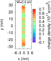
|
d) 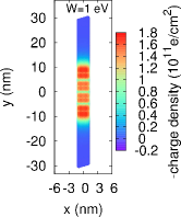
|
e) 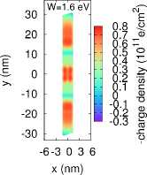
|
f) 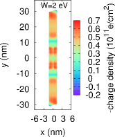
|
III.2 Charging the nanoribbon quantum dot
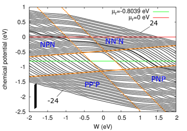
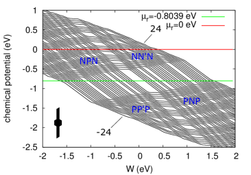
In Fig. 3(a,c) we plotted the chemical potentials for the homogenous nanoribbon with [Fig. 3(a)] and [Fig. 3(c)] atoms across the channel. The considered number of excess electrons varies between and . For a system in contact with an external electron reservoir the ribbon will be charged by electrons up to the electrochemical potential of the reservoir , i.e. the ribbon will contain electrons for , tarucha . A necessary condition for the current flow at low bias is , otherwise the charge transfer across the system is in the Coulomb blockade regime. The horizontal green line in the Fig. 3(a,c) marks meV, which is the value of the Fermi energy calculated for the neutral ribbon . This value – as we find – is independent of the size of the ribbon and corresponds to the center of the gap at the chemical potential spectrum for , and can be treated as the charge neutrality point for the interacting system. The chemical energy gap – corresponding to the gap in the transport experiments han ; chiu ; stampfer ; xliu ; nrb3 – for the ribbon with 36 atoms across is increased from 268.5 meV [Fig. 2] to 304.7 meV [Fig. 3(c)] by the electron-electron interaction. The chemical potential spectra – calculated with the restricted basis – are perfectly symmetric with respect to the point inversion across the center of the energy gap. The electron-hole symmetry found in this result is quite remarkable, given that the frozen orbitals correspond entirely to the valence band.
Note, that the present calculation deals only with the ground state of the electron system with excess electrons within the dot. The gap in Fig. 3(a) appears in the chemical potentials for varied electron numbers and not between the excited states of the single-electron or quasiparticle spectrum gap1 ; gap2 ; gap3 . The chemical potential gap determines the charging properties of the system and not – for instance – the optical ones Yamamoto ; Guclu for a fixed confined charge.
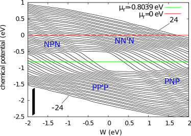
In the experimental conditions the center of the chemical potential gap can be set above or below the electrochemical potential of the external reservoir depending on the back gate potential. For below (above) this value, the ribbon outside the QD displays a -type (-type) conductivity. On the other hand the external potential (12) forms a confinement for conduction band electrons for or for valence band electrons (). For meV and we have n-type conductivity in the ribbon outside the quantum dot and confinement of the electrons of the valence band (-type) within the quantum dot. This case is labeled by ’NPN’ in Fig. 3(a,c,e,g). Other cases of confinement are denoted in a similar manner.
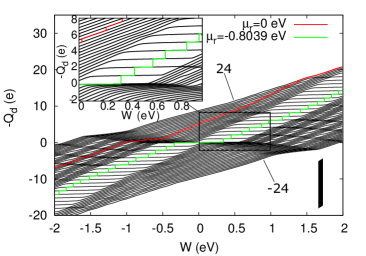
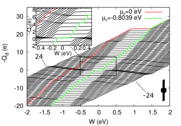
The electrons added to the nanoribbon fill the energy levels up to the electrochemical potential of the external reservoir , but do not necessarily charge the quantum dot itself. The charge confined in the quantum dot – for the nanoribbon with 18 and 36 atoms across the channel– as a function of is plotted in Fig. 3(b,d) for . The value of is found by integration of the electron charge within the segment of the nanoribbon upon subtraction of the positive ions present within this region. With the green (red) line we plotted the number of excess electrons confined inside the dot for and meV. The number of confined electrons jumps in steps between the lines corresponding to a given number of electrons within the nanoribbon. For – the value above the chemical potential gap – the entire nanoribbon is filled with electrons, over the potential of the dot – see the red line Fig. 3(b,d) – and the charge within the dot takes nearly continuous and not quantized values. On the other hand for meV – the center of the gap for , the number of electrons confined within the dot takes only integer values (green line in Fig. 3(b,d)) – and corresponds to charging the quantum dot with subsequent electrons. Note, that the entire spectrum of chemical potentials in Fig. 3(a,c) is slanted, i.e. the horizontal green line in Fig. 3(a,c) gets closer to the valence (conduction) band for (). As the number of electrons inside the nanoribbon grows, so does the potential of the background electron charge, hence the slope of the spectrum, shifting up the center of the gap for .
For eV the chemical potentials of excess electrons appear within the gap of the 36-atoms wide ribbon of Fig. 3(c). The chemical potentials within the gap acquire a stronger dependence on and the charge within the dot for these electron numbers [inset in Fig. 3(d)] becomes locally independent of . For eV the chemical potentials of electrons appear inside the gap [Fig. 3(d)], and the charge near the dot approaches a constant value before the end of the ribbon [Fig. 4(b)]. For the quantum dot attracts the electrons from the entire nanoribbon and for the excess electron charge is spread all along the system. In order to inspect the correspondence between the charge localized near the dot, the excess charge in the nanoribbon and the position of the chemical potential within the gap in Fig. 3(c) we displayed in Fig. 4(a,b) the charge within the segment of the nanoribbon for a varied number of excess electrons as a function of for potentials eV and eV, respectively. For low we find that the charge in the neighborhood of the dot exceeds the number of excess electrons (see Fig. 4(a) for and Fig. 4(b) for ), and a local maximum of as a function of is formed. The excess electron density for and eV is displayed in Fig. 5(a), with the total potential plotted in Fig. 5(b). The external potential defining the quantum dot attracts also the electrons occupying the states of the valence band. The electron charge within the dot is accumulated at the expense of the neighborhood of the nanoribbon which acquires a positive charge – see Fig. 5(c). For the positive background is left along the entire ribbon up to its slanted ends (Fig. 4(a)). For eV the local maximum of is no longer present for [Fig. 4(b)]. For the excess charge is present only within the quantum dot [Fig. 5(d)]. Note, that for the electron system spontaneously forms barriers in the total DFT potential separating the quantum dot from the rest of the system [Fig. 5(f)]. The appearance of the barriers explains the saturated excess charge observed as a function of in Fig. 4(a). For the value of grows monotonically with up to the ends of the nanoribbon [see Fig. 4(b)], indicating that the excess electrons do not fit inside the quantum dot [see Fig. 5(g) for ] and are only confined due to a finite length of the nanoribbon. In this case the total potential is no longer constant outside the quantum dot [Fig. 5(h,i) for ].
Figure 6(a) shows the charge localized within the quantum dot for a fixed as a function of . The values plotted by thick lines correspond to the chemical potential in the gap of Fig. 3(a). Only within the gap the charge acquires quantized integer values.
In the experiment xliu the transport gap is observed for both the back gate potential and the top gate potential – see the black cross in Fig. 1(c) of Ref. xliu, . The gap as a function of the back gate potential xliu corresponds to the gap observed in Fig. 3(a,c,e,f) as a function of the chemical potential (or ). We marked this gap by the solid orange lines in Fig. 3(a). The transport gap related to the top gate potential [the diagonal black region in Fig. 1(c) or Ref. xliu, ] is also present in our results. The gap due to the top gate corresponds to an extension of the central gap region in the direction parallel to the slopes of chemical potentials for the states localized inside the quantum dot [dotted orange lines in Fig. 3(a)]. Let us focus on the chemical potential of 8 excess electrons [bold black line in Fig. 3(a)] as a function of the gate voltage and look at the location of the 8th electron added to the system as a function of the external (top gate) voltage. For this purpose we subtracted the total charge densities for and systems for a varied number of electrons with the results plotted in Fig. 7. For eV [Fig. 7(a)] we are in the center of the gap marked by the dashed orange lines in Fig. 3(a). The 8th electron when added to the system occupies the ribbon connections and not the quantum dot. The flow of the current across the dot is then blocked, hence the vanishing current found in Ref. xliu, for the transport gap defined by the top-gate potential. Note, that within this gap have a negligible dependence on - which also indicates that the 8th electron is localized outside the quantum dot. When we leave the transport gap [Fig. 7(b,c) for and eV] the 8-th electron occupies both the ribbon connections and the quantum dot, allowing for the flow of the current across the system. In this region the chemical potential acquires a pronounced dependence on . For eV [Fig. 7(d)] we are in the center of the gap on the Fermi energy scale (back gate of Ref. xliu, ) and the 8-th electron occupies the dot only and the variation of with the external potential is the strongest. In the region marked by the orange solid lines in Fig. 3(a) the transport across the quantum dot can occur via the dot localized states chiu ; stampfer ; moreview ; droescher , naturally provided that the ribbon connections have non-zero density of states in this energy range. When we leave the transport gap [Fig. 7(e,f) for eV and 2 eV] the electron occupies both the dot and the ribbons allowing for the electron flow across the system.
The transport gap due to the top gate potential in Fig. 1(c) of Ref. xliu depends strongly on the back gate potential. An increase of the top gate potential in Fig. 1(c) of Ref. xliu corresponds to an increase of . A more negative back gate potential in Fig. 1(c) of Ref. xliu corresponds to a more negative values of the chemical potentials in Fig. 3(a). Hence for large positive the gap appears for large negative chemical potentials in Fig. 3(a) in a correct qualitative correspondence with Fig. 1(c) of Ref. xliu , where the transport gap for large positive top gate potential appears for large negative back gate potentials.
III.3 Charging the QD induced within the graphene flake
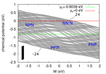
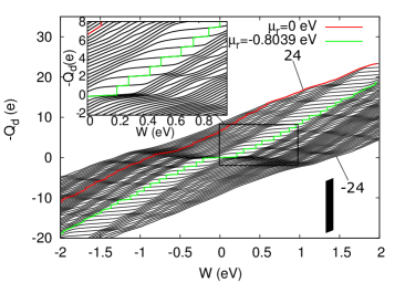
Figure 3 compares the chemical potential spectra and the charge localized within the quantum dot for a nanoribbon containing 18 atoms across the channel with [Fig. 3(e,f)] and without [Fig. 3(a,b)] a hexagonal flake defined in the center of the ribbon. For the quantum dot induced within the flake the chemical potential gap as a function of is much thinner as in the results obtained for non-interacting electrons cf. Fig. 2(a) and Fig. 2(c). The dependence of the charge confined in the quantum dot as a function of is displayed in Fig. 3(f). For a fixed value of the flake contains a larger number of electrons than for the ribbon QD [cf. Fig. 3(f) and Fig. 3(b)]. Nevertheless, no excess charge appears in the flake for a neutral system at [Fig. 3(f)]. In contrast to the nanoribbon QD – for a few extra electrons are localized within the flake QD also at . In consequence, for the flake the central band of a quantized confined charge in Fig. 3(f) is more or less constant as a function of and in contrast to the nanoribbon [Fig. 3(d)] where for , is only integer for . The plots of the confined excess charge as a function of the cutoff-radius for the flake quantum dot given in Fig. 4 indicate a large flexibility of the confinement potential in terms of the number of confined electrons. For eV [Fig. 3(f)] a saturation of the excess charge is obtained for near nm.
In order to estimate the effect of the finite size of the ribbons in the system we plotted in Fig. 3(g) and 3(h) the results for the hexagonal flake embedded in a longer ribbon. The total length of the system was increased from nm - as in Fig. 3(e,f) and elsewhere in this work, to 90 nm. We observe that the chemical potentials within the energy gap and the width of the energy gap are unchanged. Nevertheless, the chemical potentials which are outside of the gap are shifted towards the neutrality point – the band of chemical potentials for electrons becomes thinner on the vertical scale. The longer ribbons reduce the interaction energy for the carriers within the ribbons, and the chemical potential approach the continuum limit. Concerning the charge confined within the dot displayed in Fig. 3(h) – as compared to Fig. 3(f) we can see that the central part of the figure – corresponding to a quantized charge within the dot – is left unchanged. Outside the energy gap the entire nanoribbon contains a larger number of electrons for a given and the line for – as compared to Fig. 3(f) – tends to acquire a continuous dependence on . Same conclusions are reached for the charge localized within the flake quantum dot for a fixed as a function of [cf. the solid and dashed lines in Fig. 6(b) corresponding to nm and nm, respectively].
III.4 Frozen valence band charge
| a) | 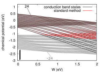 |
|---|---|
| b) | 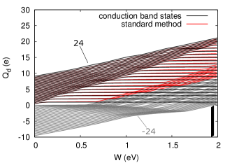 |
The results presented so far were obtained within the method in which both the conduction and valence band states formed the basis for solution of LSDA equations. Let us suppose that we are only interested in the conduction band states, or charging the quantum dot with electrons and not holes – which appears for . Let us discuss the applicability of the method with the basis limited to conduction band states – for which the complexity of the calculations can be significantly reduced. For this purpose we i) diagonalize Hamiltonian (1), ii) fix the charge density (4) as obtained for a charge neutral system taking the summation up to in Eq. (4), then iii) the LSDA equations are solved in the basis given by Eq. (3) but with summation starting from . Since the Hamiltonian (1) does not contain any potential, the frozen charge density (4) of all the occupied valence band states below the energy gap is uniform and the same on each atom of the crystal lattice. Then, the solution of the DFT equations is performed in the conduction band only, with the frozen valence charge producing only a constant potential shift, due to the exchange-correlation component of the Perdew-Zunger potential.
The results for the chemical potentials for a nanoribbon with 18 atoms across the channel are displayed in Fig. 8(a). The basis limited to the conduction band correctly reproduces the chemical potentials above and inside the gap. No additional shift was necessary to make this data coincide. As is increased, the chemical potential spectrum for low continues into the quasi-continuum of the chemical potentials of the valence band. The basis limited to the conduction band state predicts that the charge confined within the quantum dot remains quantized at integer values for large values of [black lines in Fig. 8(b)], while in the exact calculation [red lines in Fig. 8(b)] the system enters the energy continuum for the p-type conductivity. Near the bottom of the gap we find that for a fixed value of the chemical potential calculated with the limited basis goes down on the energy scale as compared to the exact calculation [Fig. 8(a)]. In this region we find that for a fixed the exact calculation gives values of the quantum-dot-confined charge which are i) larger [Fig. 8(b)] than the ones obtained with the limited basis and ii) continuous as a function on in contrast to the quantized values for the limited basis. This discrepancy is a result of filling the quantum dot by the electrons coming from the valence band from outside the quantum dot, which is present in the exact calculation but neglected in the limited basis. In the limited basis the excess charge confined within the quantum dot is underestimated, hence the underestimate of the interaction energy and in consequence lower values of chemical potentials as compared to the exact calculation [see the red and black lines in Fig. 8(a) before the black lines enter the gray band of the valence band states].
III.5 Potential profile and edge disorder
In this subsection we present the results for a modified external potential profile and the disordered edge within the flake. The choice of the form of the external potential defining the quantum dot [Eq.(12)] was taken arbitrarily, as a smooth short-range potential. In order to demonstrate that the adopted results remain qualitatively unchanged when the potential profile is varied we performed calculations for a Gaussian confinement , i.e. for a power of two instead of 4 in the exponent. The results for the chemical potential are displayed in Fig. 9 to be compared with Fig. 3(a) for the potential given by Eq. (12). The pattern of chemical potentials remains unchanged, and only quantitative differences are observed.
For the edge disorder effects we took the hexagonal flake with pure armchair edges end removed two consecutive atoms every 10 of atoms along the edge. The form of the boundary is displayed in Fig. 10(a). The edge contains fragments zigzag edge and single separated ions within armchair fragments. The results with ideal armchair edges of the flake were presented in Fig. 3(b,c) for the chemical potentials and the charge localized within the dot. Again only quantitative differences can be spotted with no overall change to the quantitative description of the effect.
| a) | 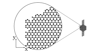 |
|---|---|
| b) | 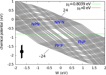 |
| c) | 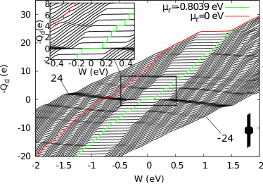 |
IV Summary and Conclusions
We have studied the charge distribution in a semiconducting graphene nanoribbon with a quantum dot defined in its center by an external potential. The calculations were performed within the tight-binding method with the electron-electron interaction introduced by the mean field DFT approach.
We determined the excess charge localized within the dot as a function of the Fermi energy and the external potential within the transport gap and outside, when the entire structure is flooded by carriers. The calculated chemical potential spectra bear signatures of the transport gaps which agree with the ones observed experimentally as functions of both the back and top gate potentials. The inline flake embedded in the gated region of the nanoribbon allows for confinement of the excess charge already in the absence of the external potential, however no excess charge within the flake is found for a charge-neutral system unless an external potential is present. We found that for the frozen valence band charge the charging of the quantum dot with excess electrons can be quite well described for above the lower limit of the transport gap. However, the lower limit of the transport gap is overlooked by the basis limited to the conductance band states. Moreover, the limited basis neglects the QD charging with the valence band electrons which appears for large external potentials. The neglect leads to an underestimate of both the confined charge and the chemical potential, particularly near the lower limit of the transport gap and below on the Fermi energy / potential scale.
Acknowledgements
This work was supported by National Science Centre according to decision DEC-2013/11/B/ST3/03837 and by PL-GRID infrastructure.
References
- (1) A.H. Castro Neto, F. Guinea, N. M. R. Peres, K. S. Novoselov, and A. K. Geim, Rev. Mod. Phys. 81, 109 (2009).
- (2) O. Klein, Z. Phys. 53, 157 (1929).
- (3) A.F. Young and P. Kim, Nature Physics 5, 222 (2009).
- (4) K. Nakada, M. Fujita, G. Dresselhaus, and Mildred S. Dresselhaus, Phys. Rev. B 54, 17954 (1996).
- (5) K. Wakabayashi, Phys. Rev. B 64 , 125428 (2001).
- (6) L. Brey, and H. A. Fertig, Phys. Rev. B 73, 235411 (2006).
- (7) K. Wakabayashi,Y. Takane, M. Yamamoto, and M. Sigrist, New J. Phys 11, 095016 (2009).
- (8) P. G. Silvestrov and K. B. Efetov, Phys. Rev. Lett. 98, 016802 (2007).
- (9) M. Y. Han, B. Özyilmaz, Y. B. Zhang, P. Kim, Phys. Rev. Lett. 98, 206805 (2007).
- (10) F. Molitor, A. Jacobsen, C. Stampfer, J. Güttinger, T. Ihn, K. Ensslin, Phys. Rev. B 79, 075426 (2009).
- (11) B. Trauzettel, D. V. Bulaev, D. Loss, and G. Burkard, Nat. Phys. 3, 192 (2007).
- (12) J. B. Oostinga, B. Sacépé, M. F. Craciun, and A. F. Morpurgo, Phys. Rev. B 81, 193408 (2010).
- (13) X. Liu, J. B. Oostinga, A. F. Morpurgo, and. L. M. K. Vandersypen, Phys. Rev. B 80, 121407(R) (2009).
- (14) C. Stampfer, J. Güttinger, S. Hellmüller, F. Molitor, K. Ensslin, and T. Ihn, Phys. Rev. Lett. 102, 056403 (2009); C. Stampfer, J. Güttinger, F. Molitor, D. Graf, K. Ensslin, and T. Ihn, Appl. Phys. Lett. 92 012102 (2008).
- (15) F. Molitor, J. Güttinger, C. Stampfer, S. Dröscher, A. Jacobsen, T. Ihn, and K. Ensslin, J. Phys. Condens. Matter 23 243201 (2011).
- (16) S. Dröscher, H. Knowles, Y. Meir, K. Ensslin, and T. Ihn, Phys. Rev. B 84, 073405 (2011).
- (17) Z. H. Chen, Y. M. Lin, M. J. Rooks, P. Avouris, Physica E 40, 228 (2007).
- (18) M. Evaldsson, I. V. Zozoulenko, H. Xu, and T. Heinzel, Phys. Rev. B 78, 161407(R) (2008).
- (19) F. Sols, F. Guinea, and A.H. Castro Neto, Phys. Rev. Lett. 99, 166803 (2007).
- (20) K.L. Chiu, M.R. Connolly, A. Cresti, C. Chua, S.J. Chorley, F. Sfigakis, S. Milana, A.C. Ferrari, J.P. Griffiths, G.A.C. Jones, and C.G. Smith, Phys. Rev. B 85, 205452 (2012).
- (21) M.Y. Han, J.C. Brant, and P. Kim, Phys. Rev. Lett. 104, 056801 (2010).
- (22) K. Todd, H.T. Chou, S. Amasha, and D. Goldhaber-Gordon, Nano Lett. 9, 416 (2009).
- (23) P. Gallagher, K. Todd, and D.Goldhaber-Gordon, Phys. Rev. B 81, 115409 (2010).
- (24) J. Güttinger, C. Stampfer, S. Hellmueller, F. Molitor, T. Ihn, and K. Ensslin, Appl. Phys. Lett. 93, 212102 (2008).
- (25) S. Schnez, J. Güttinger, M. Hueffner, C. Stampfer, K. Ensslin, and T. Ihn, Phys. Rev. B 82, 165445 (2010).
- (26) J. Güttinger, J. Seif, C. Stampfer, A. Capelli, K. Ensslin, and T. Ihn, Phys. Rev. B 83, 165445 (2011).
- (27) T. Yamamoto, T. Noguchi, and K. Watanabe, Phys. Rev. B 74, 121409 (2006).
- (28) J. Fernández-Rossier and J. J. Palacios, Phys. Rev. Lett. 99, 177204 (2007).
- (29) Z. Z. Zhang, K. Chang, and F. M. Peeters, Phys. Rev. B 77, 235411 (2008).
- (30) B. Wunsch, T. Stauber, and F. Guinea, Phys. Rev. B 77, 035316 (2008).
- (31) A. D. Güçlü, P. Potasz, and P. Hawrylak, Phys. Rev. B 82, 155445 (2010).
- (32) P. Potasz, A. D. Güçlü, and P. Hawrylak, Phys. Rev. B 81, 033403 (2010).
- (33) W. L. Wang, O. V. Yazyev, S. Meng, and E. Kaxiras, Phys. Rev. Lett. 102, 157201 (2009).
- (34) M. Zarenia, A. Chaves, G. A. Farias, and F. M. Peeters, Phys. Rev. B 84, 245403 (2011).
- (35) M. Ezawa, Phys. Rev. B 77, 155411 (2008).
- (36) P. Potasz, A. D. Güçlü, A. Wȯjs, and P. Hawrylak, Phys. Rev. B 85, 075431 (2012).
- (37) S. Moriyama, Y. Morita, E. Watanabe, and D. Tsuya, Appl. Phys. Lett. 104, 053108 (2014).
- (38) K.A. Guerrero-Becerra and M. Rontani, Phys. Rev. B 90, 125446 (2014).
- (39) G. Giavaras and F. Nori, Appl. Phys. Lett. 97, 243106 (2010).
- (40) G. Giavaras and F. Nori, Phys. Rev. B 83, 165427 (2011).
- (41) X. Li, X. Wang, L. Zhang, S. Lee, and H. Dai, Science, 319, 1229 (2008)
- (42) X. Wang, Y. Quyang, X. Li, H. Wang, J. Guo, and H. Dai Phys. Rev. Lett. 100 206803 (2008).
- (43) S. Bednarek, B. Szafran, K. Lis and J. Adamowski, Phys. Rev. B 68, 155333 (2003).
- (44) S. Bednarek, B. Szafran, and J. Adamowski, Phys. Rev. B 61, 4461 (2000).
- (45) J.P. Perdew and A. Zunger, Phys. Rev. B 23, 5048 (1981).
- (46) Broyden, C. G, Math. Comp. 19, 577 593 (1965).
- (47) I. Schnell, G. Czycholl, and R. C. Albers, Phys. Rev. B 65, 075103 (2002); S. Schulz, S. Schumacher, and G. Czycholl Phys. Rev. B 73, 245327 (2006).
- (48) D. A. Siegel,Cheol-Hwan Park, C. Hwang, J. Deslippe, A. V. Fedorov, S.G. Louie and A. Lanzara, Proc. Nat. Acad. Sci. 12, 11365 (2011).
- (49) L. P. Kouwenhoven, D. G. Austing and S. Tarucha, Rep. Prog. Phys. 64, 701 (2001).
- (50) Y.-W. Son, M.L. Cohen, and Steven G. Louie, Phys. Rev. Lett. 97 216803 (2006).
- (51) V. Barone, O. Hod, and G.E. Scuseria, Nano Lett. 6, 2748 (2006).
- (52) L. Yang, C.-H. Park, Y.-W. Son, M.L. Cohen, and S.G. Louie, Phys. Rev. Lett. 99 186801 (2007).