Broadband architecture for galvanically accessible superconducting microwave resonators
Abstract
In many hybrid quantum systems, a superconducting circuit is required that combines DC-control with a coplanar waveguide (CPW) microwave resonator. The strategy thus far for applying a DC voltage or current bias to microwave resonators has been to apply the bias through a symmetry point in such a way that it appears as an open circuit for certain frequencies. Here, we introduce a microwave coupler for superconducting CPW cavities in the form of a large shunt capacitance to ground. Such a coupler acts as a broadband mirror for microwaves while providing galvanic connection to the center conductor of the resonator. We demonstrate this approach with a two-port -transmission resonator with linewidths in the MHz regime () that shows no spurious resonances and apply a voltage bias up to V without affecting the quality factor of the resonator. This resonator coupling architecture, which is simple to engineer, fabricate and analyse, could have many potential applications in experiments involving superconducting hybrid circuits.
Embedding a quantum system, such as a qubit, in a microwave resonator is an attractive and commonly used approach. Resonators provide isolation that shields the system from environmental noise and can controllably inhibit spontaneous decay. At millikelvin temperatures, microwave resonators are in their ground state, free of entropy, while still providing microwave frequency access to read-out and manipulate quantum states. There is a wide range of hybrid systems exploring new quantum phenomena and technologies that require a microwave resonator that also offers DC-access to the device, including coupling mechanical resonators to qubits LaHaye et al. (2009); Pirkkalainen et al. (2013), microwave storage and conversion circuits Andrews et al. (2015), Josephson and quantum dot radiation Hofheinz et al. (2011); Rokhinson, Liu, and Furdyna (2012); Chen et al. (2014); Liu et al. (2015), spin qubits Petersson et al. (2012), circuits coupled to ultra cold atoms Bothner et al. (2013), and more Xiang et al. (2013). A cavity with galvanic access allows the possibility to measure simultaneously a device’s DC response, such as a current-voltage curve, and its microwave response, like emitted radiation or scattering characteristics. Such a setup could form a bridge between DC quantum transport measurements and all-microwave setups employed in circuit QED, with a wide range of applications from the study of topological and other exotic junctionsMoore (2012), to superconducting molecular junctionsSköldberg et al. (2008), to carbon nanotubesRanjan et al. ; Schneider et al. (2012).
While attractive for many applications, applying a DC current or voltage bias to a superconducting resonator without sacrificing its quality factor is a non-trivial challenge Chen et al. (2011); Li and Kycia (2013); de Graaf et al. (2014); Hao, Rouxinol, and LaHaye (2014). The first approach to incorporate DC-control into a superconducting microwave resonator was to access the resonator galvanically at a voltage node with a bias line made from a -section of transmission lineChen et al. (2011). If the frequencies of resonator and the bias line are perfectly matched, then the bias line loads the circuit with an infinite impedance (an effective open), resulting in no leakage of the microwave field on resonance. However, off-resonant circuit excitations, such as a detuned qubit, are free to decay into the bias-line. This issue was addressed recentlyHao, Rouxinol, and LaHaye (2014) using a reflective T-filter, making the suppression band a few GHz wide and reaching quality factors , at the cost of increased complexity. The insertion of the bias into a symmetry point, typically breaking ground plane symmetry, makes these designs susceptible to slot-line modes and spurious resonances. Particularly for more complex circuits, these resonances can complicate design, operation and analysis of the device. In a third approachde Graaf et al. (2014), a lumped element resonator circuit was split symmetrically in two such that a DC voltage can be applied to the two halves using isolated ground planes without any radiation losses, leading to high quality factors for perfectly balanced designs.
Here, we explore a different approach in which we replace the typical gap capacitor used as an input coupler in CPW cavities with a large shunt capacitance to ground. Doing so, we achieve a highly reflective microwave mirror in which the center conductor of the waveguide is still galvanically connected to the input line, allowing the application of a DC current or voltage. Such a design has several advantages: in contrast to resonant filter designs, the reflectivity is broadband up to the self-resonance frequency of the shunt capacitor. As no extra port is required for the DC-signal, any energy that leaks through the bias line can contribute to the measurement signal. Finally, this approach does not rely on any symmetry considerations of the cavity, simplifying design and analysis.
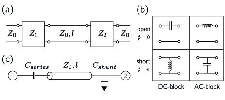
Fig. 1 shows a schematic of a generic transmission line cavity, consisting of a waveguide that is isolated from the input and output ports by impedance mismatches. At the impedance mismatch points, the propagating waves in the transmission line are reflected and a standing wave forms at resonance. Depending on the choice of impedance mismatch, one creates a boundary condition for the microwave field corresponding to either a voltage node (short), or a current node (open). To couple the cavity to external circuitry one, or both, of the boundary conditions are relaxed, which causes part of the power to be transmitted. In microwave cavities, a voltage node can be implemented by a short to ground, while a current node by a gap capacitor. These also have analogues in optical cavities: for optics, a short circuit boundary can be implemented by a semi-silvered mirror, while an open-circuit boundary can be implemented by a magnetic mirrorEsfandyarpour et al. (2014).
In CPW microwave resonators, partially transmitting impedance mismatches are typically implemented using lumped-element components such as inductors or capacitors. In general, there are four types of lossless couplers possible, which are depicted in Fig. 1b. Depending on the choice and configuration of the inductor or capacitor one obtains unity reflection () in the limit (DC-block) or (AC-block). Including that reflection on a short causes a -phase shift, each quadrant of Fig.1b can be classified according to its scattering behaviour as , in the appropriate limit bos .
| [fF] | [nH] | [pF] | [pH] | ||
|---|---|---|---|---|---|
| .5 | 3.14 | 318 | 3.18 | 1.27 | 796 |
| .9 | 254 | 35.4 | 28.6 | 11.5 | 88.4 |
| .99 | 3.22 | 315 | 126 | 8.03 | |
| .999 | .319 | 3180 | 1272 | 0.79 |
For a CPW resonator made from a transmission line coupled to a single external port, both of impedance , the coupling quality factor for all four types of couplers can be written in the following unified form bos :
| (1) |
where is the normalized susceptance of the coupler with for capacitive couplers and for inductive couplers, with for a series / shunt configuration respectively. In Table 1 we tabulated the values of the inductor and capacitor components required to achieve typical values and reflectivities .
In choosing which microwave coupler is most suitable for galvanic access, either the series inductor or the shunt capacitor, consideration of stray reactance is important. For example, a resonator with coupled with a series inductor would require an inductance of nH with a self-resonance frequency above the cavity resonance. Realizing such a high on-chip inductance with a self-resonance frequency above GHz is not practical using geometric inductance, and requires high kinetic inductance nano-inductors Annunziata et al. (2010) or Josephson junction arrays Castellanos-Beltran et al. (2008); Manucharyan et al. (2009), which suffer from limiting dynamic range and can complicate operation due to their non-linear nature. In contrast, using an on-chip parallel plate capacitor, as we will show here, it is possible to engineer a large capacitance with small stray inductance using conventional thin-film technologies.
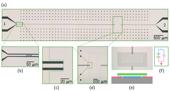
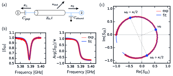
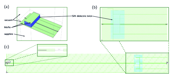
As a proof of principle, we demonstrate the concept of a shunt capacitor microwave mirror using a -transmission cavity that incorporates one shunt capacitor and one series capacitor, shown schematically in Fig.1c. Fig. 2 shows an optical microscope image of the device using a CPW cavity and an on-chip parallel plate capacitor. The devices are fabricated in a three step e-beam lithography process. First we pattern the resonator on sapphire using a layer of nm of sputtered Molybdenum-Rhenium alloy with reactive-ion etchingSingh et al. (2014). Subsequently we deposit nm of PECVD , which is wet-etched using HF. The upper plate of the capacitor is patterned in a lift-off process using PMMA and a MoRe film of nm. The resulting top plate acts as a capacitive coupler between the center conductor and the ground plane, see Fig. 1e-f. We estimate the parallel plate contribution to the shunt capacitance to be 27 pF and a stray capacitance from the lower capacitor electrode to the ground plane of pF. From formula 1, we estimate . Using finite element analysis simulationsbos , we estimate the first self-resonance frequency of the capacitor to be GHz, significantly above the cavity frequency. From equation 1, we need a gap capacitance at port 1 of fF to obtain a symmetrically coupled cavity.
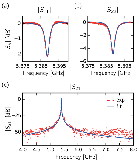
For the microwave characterization, we cool the device to mK in a radiation-tight microwave box. Using two identical cryogenic microwave reflectometry configurations connected to both ports bos , we measure the full -matrix of our device. We apply a DC voltage to the center conductor of our cavity using a bias tee attached to port 2. Fig. 3a shows a measurement of the reflection from port 1 () with a resonance at GHz, and a linewidth of MHz. This demonstrates we are able to make superconducting microwave resonators with loaded quality factors in the range of that are galvanically accessible through a frequency non-selective (non-resonant) connection.
In addition to measuring the cavity through the gap capacitance, we can also use the shunt capacitor as a partially transmitting mirror. Fig. 3b shows a measurement of the cavity resonance through the shunt capacitor. We observe a resonance at the same frequency and linewidth, demonstrating that the coupler works as a mirror. From the fit bos , we find a coupling , giving an effective capacitance of pF. With the fits of both reflection measurements we can extract the coupling rates for each port bos . By combining these results we can extract the magnitude of the internal losses using , and find an internal loss rate of about kHz. We estimatebos a contribution of 8-80 kHz to the total internal loss rate of the cavity from the dielectric losses of the shunt capacitor, assuming a dielectric loss tangent . Reducing the dielectric thickness to 10 nm, we predictbos that this loss rate could be reduced to 0.8 kHz, limiting the internal Q of the cavity to .
In transmission, Fig.3c, we observe a single resonance, with a clean spectrum over the full measurement bandwidth of GHz, showing that this approach does not suffer from spurious resonances.
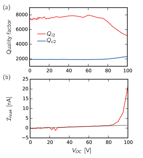
In figure 4, we characterize the performance of our cavity with a DC voltage bias applied to port 2 using a bias tee. As shown in Fig. 4a, we observe no notable effect on the microwave response up to V. The same behaviour is also observed at single photon level (input power of dBm). At V, we observe a leakage current of nA, giving a resistance of . Above V, we see the onset of dielectric break down with the leakage current rising sharply to nA, leading to an estimated breakdown field of MV/cm. Beyond 80 V, we see a degradation of the internal quality factor, corresponding to an increase of kHz to the internal loss rate. Also we observe a slight increase in the coupling quality factor to port 2, , implying an increase in the shunt capacitance of about pF. This could be caused by an inversion layer induced in the dielectric, effectively decreasing the plate separation. The increase of internal losses could be related to Ohmic losses in the inversion layer.
To conclude, we have introduced a new type of microwave coupler that allows galvanic access to the center conductor of a CPW microwave resonator. We demonstrated this concept by engineering a -transmission cavity with a high quality factor in which we can apply a large DC voltage to the center conductor of the resonator. By reducing the dielectric layer thickness to 10 nm, we predict that coupling quality factors of up to should be possible while the first the self-resonance of the capacitor appears at GHz. bos For larger capacitances the dielectric losses of the deposited dielectric contribute less than a kHz to the internal loss rate of the cavity bos , at the expensive of a reduced dielectric breakdown voltage.
The simplicity of this broadband technique together with the possibility of large quality factors suggests that this new design could be very attractive for many applications and experiments involving superconducting hybrid circuits.
The authors would like to thank Daniel Bothner, Joshua Island, Nodar Samkharadze, David van Woerkom, and Martijn Cohen for useful discussions.
References
- LaHaye et al. (2009) M. LaHaye, J. Suh, P. Echternach, K. Schwab, and M. Roukes, “Nanomechanical measurements of a superconducting qubit,” Nature 459, 960–964 (2009).
- Pirkkalainen et al. (2013) J.-M. Pirkkalainen, S. Cho, J. Li, G. Paraoanu, P. Hakonen, and M. Sillanpää, “Hybrid circuit cavity quantum electrodynamics with a micromechanical resonator,” Nature 494, 211–215 (2013).
- Andrews et al. (2015) R. Andrews, A. Reed, K. Cicak, J. Teufel, and K. Lehnert, “Quantum-enabled temporal and spectral mode conversion of microwave signals,” arXiv preprint arXiv:1506.02296 (2015).
- Hofheinz et al. (2011) M. Hofheinz, F. Portier, Q. Baudouin, P. Joyez, D. Vion, P. Bertet, P. Roche, and D. Estève, “Bright side of the coulomb blockade,” Physical review letters 106, 217005 (2011).
- Rokhinson, Liu, and Furdyna (2012) L. P. Rokhinson, X. Liu, and J. K. Furdyna, “The fractional ac josephson effect in a semiconductor-superconductor nanowire as a signature of majorana particles,” Nature Physics 8, 795–799 (2012).
- Chen et al. (2014) F. Chen, J. Li, A. Armour, E. Brahimi, J. Stettenheim, A. Sirois, R. Simmonds, M. Blencowe, and A. Rimberg, “Realization of a single-cooper-pair josephson laser,” Physical Review B 90, 020506 (2014).
- Liu et al. (2015) Y.-Y. Liu, J. Stehlik, C. Eichler, M. Gullans, J. Taylor, and J. Petta, “Semiconductor double quantum dot micromaser,” Science 347, 285–287 (2015).
- Petersson et al. (2012) K. Petersson, L. McFaul, M. Schroer, M. Jung, J. Taylor, A. Houck, and J. Petta, “Circuit quantum electrodynamics with a spin qubit,” Nature 490, 380–383 (2012).
- Bothner et al. (2013) D. Bothner, M. Knufinke, H. Hattermann, R. Wölbing, B. Ferdinand, P. Weiss, S. Bernon, J. Fortágh, D. Koelle, and R. Kleiner, “Inductively coupled superconducting half wavelength resonators as persistent current traps for ultracold atoms,” New Journal of Physics 15, 093024 (2013).
- Xiang et al. (2013) Z.-L. Xiang, S. Ashhab, J. You, and F. Nori, “Hybrid quantum circuits: Superconducting circuits interacting with other quantum systems,” Reviews of Modern Physics 85, 623 (2013).
- Moore (2012) J. E. Moore, “Viewpoint: An extraordinary josephson junction,” Physics 5, 84 (2012).
- Sköldberg et al. (2008) J. Sköldberg, T. Löfwander, V. S. Shumeiko, and M. Fogelström, “Spectrum of andreev bound states in a molecule embedded inside a microwave-excited superconducting junction,” Physical review letters 101, 087002 (2008).
- (13) V. Ranjan, G. Puebla-Hellmann, M. Jung, T. Hasler, A. Nunnenkamp, M. Muoth, C. Hierold, A. Wallraff, and C. Schönenberger, “Clean carbon nanotubes coupled to superconducting impedance-matching circuits,” Nature communications 6, doi:10.1038/ncomms8165.
- Schneider et al. (2012) B. Schneider, S. Etaki, H. van der Zant, and G. Steele, “Coupling carbon nanotube mechanics to a superconducting circuit,” Scientific reports 2 (2012).
- Chen et al. (2011) F. Chen, A. Sirois, R. Simmonds, and A. Rimberg, “Introduction of a dc bias into a high-q superconducting microwave cavity,” Applied Physics Letters 98, 132509 (2011).
- Li and Kycia (2013) S.-X. Li and J. Kycia, “Applying a direct current bias to superconducting microwave resonators by using superconducting quarter wavelength band stop filters,” Applied Physics Letters 102, 242601 (2013).
- de Graaf et al. (2014) S. E. de Graaf, D. Davidovikj, A. Adamyan, S. Kubatkin, and A. Danilov, “Galvanically split superconducting microwave resonators for introducing internal voltage bias,” Applied Physics Letters 104, 052601 (2014).
- Hao, Rouxinol, and LaHaye (2014) Y. Hao, F. Rouxinol, and M. LaHaye, “Development of a broadband reflective t-filter for voltage biasing high-q superconducting microwave cavities,” Applied Physics Letters 105, 222603 (2014).
- Esfandyarpour et al. (2014) M. Esfandyarpour, E. C. Garnett, Y. Cui, M. D. McGehee, and M. L. Brongersma, “Metamaterial mirrors in optoelectronic devices,” Nature nanotechnology 9, 542–547 (2014).
- (20) See supplementary material.
- Annunziata et al. (2010) A. J. Annunziata, D. F. Santavicca, L. Frunzio, G. Catelani, M. J. Rooks, A. Frydman, and D. E. Prober, “Tunable superconducting nanoinductors,” Nanotechnology 21, 445202 (2010).
- Castellanos-Beltran et al. (2008) M. Castellanos-Beltran, K. Irwin, G. Hilton, L. Vale, and K. Lehnert, “Amplification and squeezing of quantum noise with a tunable josephson metamaterial,” Nature Physics 4, 929–931 (2008).
- Manucharyan et al. (2009) V. E. Manucharyan, J. Koch, L. I. Glazman, and M. H. Devoret, “Fluxonium: Single cooper-pair circuit free of charge offsets,” Science 326, 113–116 (2009).
- Singh et al. (2014) V. Singh, B. H. Schneider, S. J. Bosman, E. P. Merkx, and G. A. Steele, “Molybdenum-rhenium alloy based high-q superconducting microwave resonators,” Applied Physics Letters 105, 222601 (2014).
- Pozar (2009) D. M. Pozar, Microwave engineering (John Wiley & Sons, 2009).
Supplementary Material: Broadband architecture for galvanically accessible superconducting microwave resonators
Sal J. Bosman1, Vibhor Singh1, Alessandro Bruno1,2, Gary A. Steele1
1Kavli Institute of NanoScience, Delft University of Technology,
PO Box 5046, 2600 GA, Delft, The Netherlands.
2Qutech Advanced Research Center, Delft University of Technology,
Lorentzweg 1, 2628 CJ Delft, The Netherlands.
S1 Measurement setup
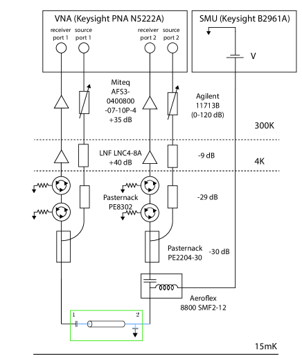
The complete measurement setup used for the device characterization is shown schematically in Fig. S1. It consists of two identical microwave reflectometry measurement chains, such that we have full access to the scattering matrix of the device (). The vector network analyser (VNA) outputs a signal that is fed through a variable attenuator at room temperature into the fridge, where it is first heavily attenuated before reaching the sample through a directional coupler. The reflected signal from the device is sent back to the VNA using two isolators and amplifiers. From each reflectometry setup we can measure the reflection of that port and by combining them we can measure transmission in both directions. Additionally we can apply a DC voltage to port 2 of the device through an unfiltered DC-line using a bias-tee just before the device.
S2 Microwave circuit analysis
For two-port components, as depicted in Fig.1b of the main text, the transmission matrices, or -matrices are of the form [S1]:
| (S2) |
These matrices relate incoming voltages and currents of port 1 () to outgoing () from port 2, hence characterize transmission of the two-port network. From these matrices we can already understand the limiting behaviour stated in the main text. If one takes the limit wherein the off-diagonal element goes to zero, the component shows perfect transmission. And in the limit where the off-diagonal element diverges, all power is reflected. The minus sign for reflection of a shunt component is due to the reversed sign of in -matrices compared to scattering matrices (i.e. the current flows out of port 2). Using standard formulas we can rewrite into explicit scattering parameters for each component as:
| (S3) |
Using these expressions the reflection coefficient of port i, , can easily be calculated, where is the normalized impedance and () for the capacitor (inductor), with the imaginary unit. It is perhaps interesting to note that the beam splitter condition (), for such a two-port component embedded in a transmission line (TL) needs a impedance for a shunt and for a series component
To derive formula 1 in the main text we need to determine the coupling quality factor for each of the four coupler types for a single-port -microwave resonator. A resonator requires opposite boundary conditions on each end of the TL, hence the open type of couplers are connected to a shorted TL and vice versa for the short type of couplers.
Following reference [S1], here we present the generalized case. First we consider the open types of terminations; the gap capacitor and series inductor. In this configuration we have the coupler in series with a shorted TL, which has an impedance of , with the length of the TL and , where is the phase velocity and the imaginary unit. At resonance we have , and the input impedance diverges. Now the impedance of the coupled resonator seen from the feedline is , with the impedance of the coupler, either or . To perform a Taylor expansion around the resonance, where diverges it is convenient to rewrite it in terms of the susceptance of the coupler and the cotangent. Note that for capacitors and for inductors , which we abbreviate as (upper sign corresponds to an inductive element and the lower sign for a capacitive element). Now we can write the input impedance as follows:
The last approximation breaks down for very large coupling susceptances. Remark that we used the trigonometric identity to rewrite . In this way we could invoke the resonance condition. For a low loss resonator we can include internal losses by substitution of in the numerator and obtain:
| (S4) |
This expression of the input impedance is equivalent to that of a series LC-resonator, with a resistance on resonance of . At critical coupling the resonator on resonance is impedance matched to the feedline, and equals , which is captured with the coupling factor . Now using we obtain the result:
| (S5) |
For the shunt couplers the derivation is very similar. Now we consider a shunt inductor () or a shunt capacitor () coupled to an open ended TL, with . Now we have a parallel circuit so we obtain:
| (S6) |
We see that if we replace and reverse the sign we obtain the same expression, though in admittance . This shows that such coupled cavities behave as parallel LC-resonators. Following the same logic we obtain:
| (S7) |
with (+) for capacitors and (-) for inductors respectively. So we conclude that for the shunt couplers we obtain:
| (S8) |
In the derivation for the series couplers we used , since for example a 10 fF gap capacitor in a 5 GHz cavity of 50 Ohms is , making the approximation valid. In the case of the shunt capacitor the reasoning goes exactly in opposite direction, where , in the case of 30 pF for the same cavity we obtain , justifying this approximation.
S3 Microwave response
With the expression for the input impedance at hand, it is easy to derive the microwave response of the cavity in reflection. Each coupling port contributes to the total loss rate and causes a small shift of the resonance frequency, which is here not of our interest. In our implemented microwave cavity, as depicted in Fig. 1c and Fig. 2 of the main text, we can distinguish three separate loss channels that contribute to the total linewidth of the cavity: . A reflection measurement on port is sensitive to the ratio between the total linewidth and coupling rate to port , captured with the coupling coefficient: . Therefore if we absorb the coupling rate of the other port into we can suffice using the previously derived expressions. The reflection of the effective single-port cavity can then be written as:
| (S9) |
Using that and similar for we can rewrite (formula S3) as follows:
| (S10) |
Combining both expressions and rearranging the ’s we obtain:
| (S11) |
The reflection response on port 2 () is very similar, with the only difference that it was written in admittance. Here we will use as the input impedance for port 2:
| (S12) |
Following the same logic as before we obtain:
| (S13) |
For deriving the transmission response one cannot use this trick and the cavity should be analysed using transfer matrices. By multiplying the -matrices of the gap-coupler, the TL and shunt coupler, one arrives at the -matrix for the full cavity, from which an expression for can be determined. If we abbreviate and , and follow a similar procedure as before we obtain:
| (S14) |
This expression can then be simplified to:
| (S15) |
and we have obtained all response functions. For reflection of the gap capacitor (, formula S10) with a large detuning from the resonance frequency, the response is anchored at the point in the complex plane, which shows that the reflection on a (quasi)-open does not cause a phase shift of the signal. The response of the shunt capacitor, described by formula S12, is anchored at , showing the phase shift on a (quasi)-short boundary condition. Transmission, , for a large detuning is anchored at the origin, indicating there is no transmission of very off-resonant signals.
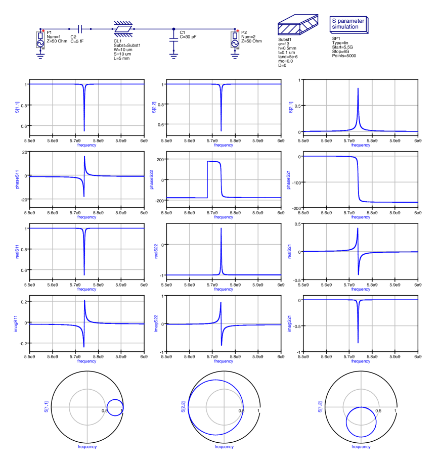
Close to resonance the term becomes important and the response will trace a (resonance) circle in the complex plane, where the radius depends on the coupling coefficient . For an over-coupled port () the resonance circle will enclose the origin and the phase angle will change by , whereas the phase angle of an under-coupled port will remain on the same branch. We would like to make a cautionary note on interpretting phase data without inquiring the resonance circle, as the ‘unwrapping’ of different phase branches is arbitrary and can lead to erroneous conclusions. At resonance the magnitude of the reflection response will show a minimum (dip) of magnitude . After determining whether the port is under- or over-coupled, can be found by measuring the depth of the resonance dip. To illustrate the differences in the microwave response we show the results of a simulation in QUCs (an open-source circuit simulator [S2]) in Fig. S2.
S4 Data analysis
Here we demonstrate the data analysis with the reflection data of port 2. Experimental realities like cable resonances and other uncontrolled factors in the circuitry can change the response from a Lorentzian line shape to a skewed-Lorentzian or Fano-line shape. This can be captured by the following adaptation of formula S12:
| (S16) |
where , and account for an offset of the anchor of the resonance circle. Taking these effects correctly into account is non-trivial and described for example in [S3,S4].
As the transmission response is insensitive to such effects, we first determine the total linewidth by fitting to formula S14 and obtain MHz. Subsequently we can fit the reflection data as shown in Fig. S3 for and determine the coupling rates. From these fits we obtain MHz () and MHz (). Using , we extract the internal loss rate as kHz, corresponding to a .
S5 Shunt capacitor simulations
In this section we explore the implications of using the shunt-capacitor coupling architecture on the (potential) performance of a microwave resonator. First we discuss the simulation setup used, and follow with discussing the self-resonances of the shunt capacitor, losses incurred by the dielectric of the capacitor and maximum obtainable Q-factors.
S5.1 Sonnet simulation setup
Sonnet is simulation software specialized in planar microwave circuits. Both the full cavity and the shunt capacitor are simulated separately, as depicted in Fig. S4. To allow simulations on a m grid we implemented the input coupler as an ideal capacitor of 10 fF. We used a kinetic (sheet) inductance of for the Molybdenum-Rhenium layers based on earlier measurements for similar films [S5]. For the SiN brick we used , and defined degrees of freedom per lattice point in the -direction.
S5.2 Low frequency response
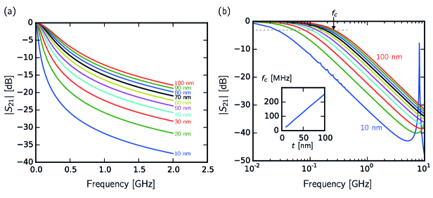
Here we simulate the low frequency response of the shunt capacitor as a function of thickness. In this configuration it can be considered as a single-pole low-pass filter, which enables us to determine the capacitance from its cut-off frequency. For applications it can be used to determine the required DC-filtering to protect potential circuits against low frequency noise. Fig. S5a shows that by decreasing the thickness of the dielectric the transmission for high frequencies is more suppressed, which is expected as in the parallel plate approximation. More instructive is to consider the transmission on a logarithmic frequency scale, as depicted in Fig. S5b, known as a Bode plot. We observe the slope to be close to 20 dB/octave, characteristic of a single-pole low pass filter. Using a RC-circuit model we can determine the capacitance from the cut-off frequency using , where because both ports are in parallel. For nm we determine a cut-off frequency of 255 MHz, corresponding to 25 pF of capacitance, close to the 27 pF we expect from a parallel plate approximation.
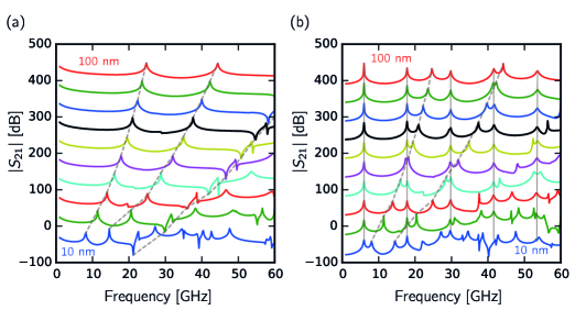
S5.3 Self-resonance frequency
In the previous section we observed that for a 10 nm dielectric a self-resonance of the shunt capacitor due to stray inductance appeared around GHz. These self-resonances place an upper bound to achievable ’s, because the coupling quality-factor increases as the total capacitance increases. To determine the maximum obtainable coupling Q for a cavity and a shunt capacitor of this geometry, we study these self-resonances as shown in Fig. S6. The first resonance drops from GHz for a nm thickness, to GHz for nm thickness. Thus for circuits requiring coupling Q’s in access of , corresponding nm, one needs to take measures to prevent these resonances to interfere with the circuit, like increasing the impedance of the resonator or introducing structures in the shunt capacitor that prevent box modes (like via’s in a pcb).
S5.4 Dielectric losses
Deposited dielectrics are well known to be lossy with loss tangents varying from . Here we consider this contribution to the losses of a cavity using a shunt capacitor as coupler. The dielectric loss tangent is specified as , with , where denotes the dissipative part of the dielectric constant. For a lossy parallel plate capacitor, that we showed in previous sections to be a valid approximation, we can use . As a circuit this can be modelled by including an equivalent series resistor (), capturing the losses in the dielectric, where , as depicted in Fig. S7a. Now we consider a single-port cavity, as displayed in Fig. S7b, and simulate it in QUCs [S2] for various coupling capacitances and loss tangents. From the simulated scattering data we can extract the coupling rate to port , as a function of dielectric thickness, showed by the dashed line in Fig. S7. As expected decreases from about 2 MHz to 20 kHz by decreasing the dielectric thickness.
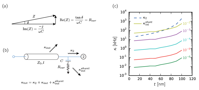
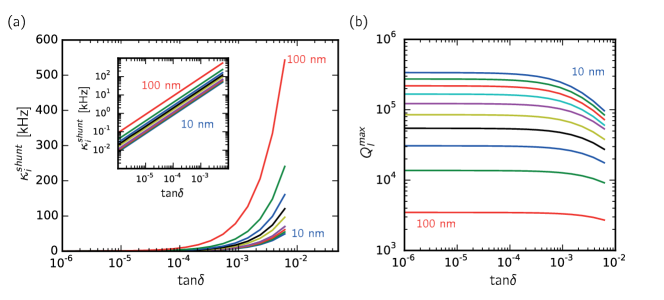
The losses incurred by the lossy dielectric capacitor can be isolated by comparing for different ’s to the lossless case, which is shown in Fig. S7c as the solid lines. These incurred losses decrease as the coupling capacitance increases, because the voltage across the capacitor plates decreases and hence the dielectric losses decrease as well. Assuming a loss tangent of around we estimate these losses in our experiment to be on the order of kHz. Finally from this figure we see that for thin dielectrics and realistic ’s the incurred losses can be minimized to sub-kHz level.
Finally we can use this data to determine what the maximum possible loaded quality factor for this resonator architecture is, shown in Fig. S8. By including both the coupling rate and dielectric losses of the capacitor, we see that the loaded quality factor is limited to for a dielectric thickness of 10 nm. Such a loaded quality factor corresponds to linewidth’s in the range of kHz, sufficiently narrow for most applications. Beyond this regime a different geometry or a higher impedance resonator is required.
[S1] D. M. Pozar, Microwave engineering (John Wiley & Sons, 2009)
[S2] M. Brinson and S. Jahn, International Journal of Numerical Modelling: Electronic Networks, Device and Fields
22, 297 (2009)
[S3] M. Khalil, M. Stoutimore, F. Wellstood, and K. Osborn, Journal of Applied Physics 111, 054510 (2012).
[S4] S. Probst, F. Song, P. Bushev, A. Ustinov, and M. Weides, Review of Scientific Instruments 86, 024706 (2015).
[S5] V. Singh, B. H. Schneider, S. J. Bosman, E. P. Merkx, and G. A. Steele, Applied Physics Letterrs 105, 222601
(2014).