Transport Conductivity of Graphene at RF and Microwave Frequencies
Abstract
We measure graphene coplanar waveguides from direct current (DC) to =13.5GHz and show that the apparent resistance (in the presence of parasitic impedances) has an dependence (where ), but the intrinsic conductivity (without the influence of parasitic impedances) is frequency-independent. Consequently, in our devices the real part of the complex alternating current conductivity is the same as the DC value and the imaginary part. The graphene channel is modeled as a parallel resistive-capacitive network with a frequency dependence identical to that of the Drude conductivity with momentum relaxation timeps, highlighting the influence of alternating current (AC) electron transport on the electromagnetic properties of graphene. This can lead to optimized design of high-speed analogue field-effect transistors, mixers, frequency doublers, low-noise amplifiers and radiation detectors.
I Introduction
Graphene is a promising material for high-frequency electronic applications, ranging from DC to THzNovoS306 ; FerrNANO7 ; VicaNM11 ; SpirAPL104 ; Sordan , such as transistorsWuN472 ; WuNL12 ; LiaoN467 ; LinNL9 ; LinS327 ; PallAPL99 ; MoonIEDL30 ; LemmIEDL28 , low-noise amplifiersDasIEEEP , mixersWangIEDL31 , frequency doublersWangIEDL31 ; YangACSN4 and microwave radiation detectorsDragJAP107 . This is because of its high carrier mobility ( at room temperatureMayo11 ), ambipolar transportNovoS306 , high Fermi velocity m/s [NovoN438, ], current carrying capacityYuNL12 (1.8) and thermal conductivityBalaNL8 (5000W). Power dissipation through a channel of resistance R carrying radio-frequency (1-300MHz) and microwave signals (0.3-300GHz) is also an important parameter, particularly for applications in high-speed electronics, such as transistors and low noise amplifiers. Any increase of channel resistance at higher frequencies (above the DC value), , will contribute excess noise and impact the signal-to-noise ratio at both the component level and when integrated into a complete system-on-chipBertz or microwave monolithic integrated circuit (MMICs)DealMM9 . The dependence of on frequency therefore needs to be determined accurately to ensure that the power dissipation does not become prohibitive for applications in a given frequency range (such as microwaves or THz). Power dissipation, e.g., degrades the signal-to-noise ratio in high-frequency detectorsDragJAP107 . Metals and superconductors show strong frequency dependence of their surface impedance which manifests as electromagnetic losses and skin effect lossesDuffBOOK , leading to an additional AC resistance.
The AC (or dynamic) conductivity of single layer graphene (SLG) from DC to optical frequencies can be modeled by the Kubo formalismKubo12 ; Ando71 ; GusyCM19 ; HansJAP103 ; KoshSSC149 ; KoshPRB87 as[FaloEPJB56, ; KoppeNL11, ]:
where T is the temperature, the reduced Planck’s constant, i the imaginary unit, the Fermi energy, the Boltzmann’s constant, and is[FaloEPJB56, ; KoppeNL11, ]:
| (2) |
Eq.I consists of intra- and inter-band contributions, corresponding to the first and second term respectively. The conductivity depends on the energy of the incident RF radiation, such that the interband term corresponds to electron-hole (e-h) pair generation and recombination events, whereas the intraband converges to the Drude model for T=0K. In the DC to 13.5GHz range, relevant for devices and applications such as transistors, mixers and low noise amplifiers, the inter-band transitions are negligible and Eq.I can be rewritten as:
| (3) | |||||
where is the electron scattering rate (in units of ) due to electron interactions with impurities, defects, phonons and disorder and is the chemical potential. Eq. (3) can be rewritten in the Drude form (at room temperature and constant and ) as [HornPRB83, ]:
| (4) |
where and are the real and imaginary components of the conductivity. The prefactor , known as the Drude weightHornPRB83 ; AbedPRB84 , is:
| (5) | |||||
for graphene is different from conventional metals due to its linear energy-wavevector dispersion (in contrast with in metals, where is the carrier effective mass and its number densityKitteBOOK ). Eq.(4) suggests that, for , graphene’s conductivity should be frequency-independent and approximately equal to the DC conductivity . Given that of SLG is in the order of 1 - 20 THz (depending on doping, material quality, i.e. exfoliated/chemical vapor deposited (CVD)), which corresponds to ps [HornPRB83, ; TanPRL99, ; MittNP11, ; LinQE20, ], graphene’s conductivity should be frequency-independent up to0.5-1THz. However, experimental confirmation of this frequency-independent response of graphene to transport RF and microwave signals has not been reported, to the best of our knowledge.
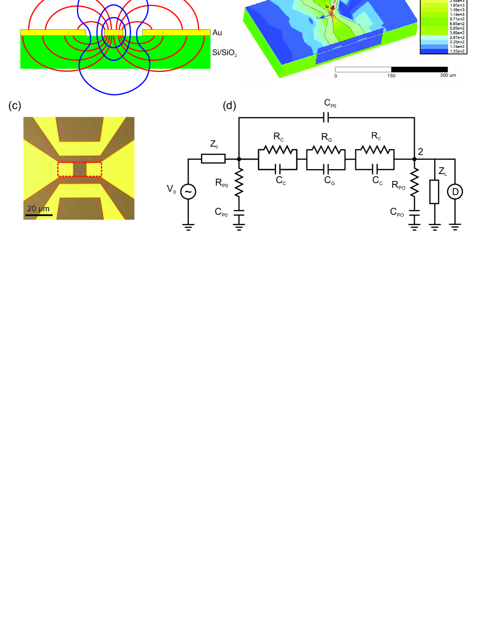
We integrate SLG into coplanar waveguide (CPW) transmission lines in order to investigate its RF and microwave transport properties. The CPW transmission lines (Fig.1 a,b) consist of a central signal conductor in close proximity with two ground conductorsWenIEEETM17 . These are ideal for investigating the RF to mm-wave electromagnetic transport properties of a variety of materials and devicesPoza , since their properties are well established theoreticallyPoza ; WenIEEETM17 and experimentallyWenIEEETM17 . Compared to microstripsPoza , CPWs enable quasi-transverse electromagnetic (TEM) wave propagation (where quasi-TEM refers to the presence of small but finite longitudinal electric and magnetic field components), low dispersion of its characteristic impedance, low cross-talk (or interference with any nearby devices) and broadband (DC to mm-wavePoza ) operation. Furthermore, CPWs can also be used as a building block for the integration of passive and active components into complete systems-on-chipBertz or MMICsDealMM9 (which integrate a range of functionalities, such as mixing, amplification, switching etc. at microwave frequencies). CPWs allow accurate measurement of RF properties, since their electromagnetic properties are traceable to well-established and extensively used Short-Open-Load-Thru (SOLT) reference standards (linked to the benchmark National Institute for Standards and Technology multiline Thru-Reflect-Line proceduresMarkITMTT39 ), provided by instrument manufactures and national metrology institutes to enable calibration of vector network analyzers (VNAs)MarkITMTT39 .
Several groups have integrated graphene with CPWs in order to investigate its electromagnetic transport properties and reported a change in the DC to AC conductivity. Ref.[MoonNJP12, ] reported from DC to 10 GHz, whereas in Ref.[LeeAPL100, ] from DC to 13.5 GHz and in Ref.[SkulAPL99, ] from DC to 13.5 GHz. These results contrast the predictions of Eqs.I-5.
Here, we report the design, fabrication and characterization of graphene CPWs (GCPWs) up to 13.5GHz. We extract their transmission line parameters and compare them with Au waveguides without the presence of graphene. We measure an intrinsic resistance and intraband conductivity of graphene frequency-independent up to 13.5GHz. This contrasts the frequency-dependent resistance of metals and superconductors at RF and microwave frequencies and can be used to design and develop broadband RF devices based on graphene.
II Results and discussion
We first design, characterize and optimize a set of Au CPWs. The width of the CPWs is fixed at having a pitch of the Ground-Signal-Ground (GSG) contact pads150 to match the GSG probe tips connected to semi-rigid coaxial cables interfaced to an Agilent N5230C VNA, with an upper frequency limit of 13.5GHz. The CPWs length is optimized to in order to accommodate the tapering of the signal conductor from its contact pad of dimensions 100 x 100 to a 10 x 10 SLG sample. The contacts are formed by evaporating 2nm Cr/80 nm Au. The optimized Au CPWs show excellent broadband RF and microwave transmission properties from DC to 13.5GHz, as discussed later.
We then fabricate GCPWs identical to the optimized AuCPWs except for the signal conductor having a gap for positioning SLG. SLG flakes are prepared by micro-mechanical cleavage of graphiteBonaMT15 ; NovoPNAS on a high resistivity () Si+ 285nm SiO2 substrate. The single layer nature of the flakes is confirmed by a combination of optical microscopyCasiNL7 and Raman spectroscopyFerrPRL97 ; FerrNN8 . Polymethyl methacrylate (PMMA) is then spin-coated onto the substrate. A frame with the desired shape is subsequently defined via e-beam lithography. After resist development, a mild oxygen plasma is used to remove the uncovered SLG parts. This results in an island of desired rectangular shape (30x10) isolated from the rest of the polymer film. The latter is then removed by immersion in de-ionized water, while the lithographically defined island remains on the substrate. PMMA is then dissolved leaving an isolated SLG flakeBonaMT15 . Cr/Au contacts are then deposited, as for Fig.2.
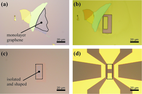
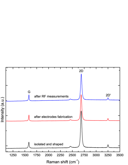
Raman spectroscopy is used at every stage of the device fabrication process and after RF measurements. Fig.3 plots representative Raman spectra (acquired in the same spot) of shaped SLG, the same SLG after contact fabrication and post RF measurements. By analyzing the position of the G peak, Pos(G), its full width at half maximum, FWHM(G), the position of the 2D peak, Pos(2D), as well as the intensity and area ratios I(2D)/I(G) and A(2D)/A(G), it is possible to conclude that the sample is p-dopedPisaNM6 ; BaskPRB80 ; DasNN3 , with a carrier concentrationcm-2 [BaskPRB80, ; DasNN3, ] and a Fermi energymeV [BaskPRB80, ; DasNN3, ]. After contact fabrication, only small changes of Pos(G) and Pos(2D) (1cm-1) occur, while I(2D)/I(G) is reduced from 6 to 4, indicating that that the doping of the sample increases during the process, but still remains below5. Doping remains unchanged after RF measurements, as indicated by no changes in peak positions, FWHMs, intensity and area ratiosPisaNM6 ; DasNN3 ; CasiAPL91 . No significant D peak is detected at any stage of the fabrication process nor after the RF measurements, proving the high structural quality of the flakes and the non-invasiveness of the measurements.
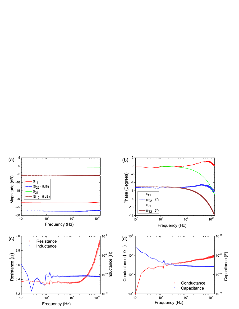
The GCPWs are first characterized at DC using a parameter analyzer in a 2-probe configuration since SLG is positioned in the signal conductor (i.e. source-drain configuration). In order to contact the SLG, the CPWs are tapered from the contact pads to match the width of the selected SLG flakes, whilst maintaining the 50 characteristic impedance of the waveguide, as shown in Fig1(c). The corresponding equivalent lumped-parameter (or discrete electrical components) model for the GCPW, together with the parasitic impedances, is shown in Fig.1(d). The lumped-parameters are based on the physical layout and geometry and are equivalent to a transmission line modelAwanBOOK ; DuffBOOK . The electrical properties of a CPW are related to its impedance Z, which depends on the geometry and dielectric properties of the surrounding medium (such as Si substrate, SiO2 layer and air). The CPW impedance is given byWenIEEETM17 where and are elliptic integrals of the first kind and their complement, is the relative permittivity of the substrate and , where is the width of the central conductor and is the width of the gap between the central and ground conductors. In Fig.1(d), the capacitance CC and resistance RC account for the two contacts (i.e. source and drain) on the SLG, while the SLG channel is modeled by a parallel resistance and capacitance, RG and CG. CPS accounts for the capacitive coupling between the two leads contacting the SLG channel. RP0 and CP0 denote the coupling between the SLG contacts and the outer ground electrodes. Fig.1(a) shows the schematic electric and magnetic field distributions when an even-mode (or transverse electromagnetic mode) is excited in the waveguide. Parasitic odd-modes (or non-TEM modes) can also be excited if, e.g., the two ground conductors are at different potentials as a result of improper or non-planar GSG contact. Fig.1(b) plots a finite element simulation (using the High Frequency Structures Simulation (HFSS) software with 1 excitation voltage between the ground and signal conductors at 13.5 GHz) of a tapered AuCPW at 13.5GHz optimized (through simulation of the waveguides with varying geometrical designs) to enable integration of SLG as the channel material. The figure shows the distribution of the surface current density at 13.5GHz in the waveguide. HFSS solves Maxwell’s equations at each mesh in the simulation domain to calculate the current density distribution on metallic and dielectric surfacesPoza .
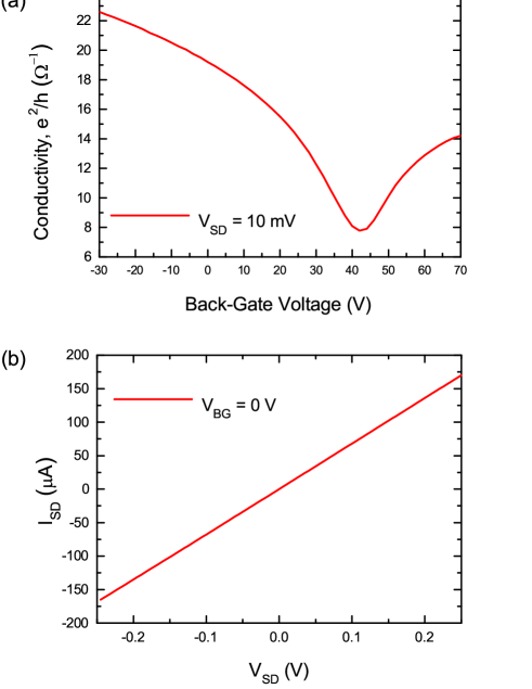
Fig.4(a) plots the two-probe DC conductivity and back-gate voltage dependence measured on our GCPW between the input and output signal conductors (or source and drain electrodes). The SLG channel dimensions are length and width , and the overlap under the Cr/Au contacts is 10 in length and width (precisely defined through e-beam lithography). The SLG channel in the waveguide is p-doped (200), consistent with the Raman analysis. The Dirac-point is detected at and corresponds to a minimum conductivity and a sheet resistance . Fig.4(b) indicates a linear dependence of on , with two-probe resistance at zero back-gate potential. All RF and microwave measurements are performed with a fixed zero back-gate potential. The corresponding carrier density and mobility are estimated as with [NovoS306, ], and , respectively, and the Fermi level 200. The carrier mean-free path can be estimated fromTanPRL99 as nm using the measured carrier concentration at DC and room temperature, indicating diffusive transport (comparable to the typically found in SLG devices on SiO2 at room temperatureAdamPNAS47 ; TanPRL99 ).
Subsequent to the DC measurements, our GCPWs are characterized at RF and microwave frequencies by measuring the magnitude and phase of the scattering-parameters, , in a two-port configuration, where , with a 2x2 S-parameters matrix. For a two-port network with characteristic impedance Z0 the impedance matrix in terms of S-parameter matrix and the identity matrix [I] is given byPoza :
| (6) |
The waveguide S-parameters are measured using a VNA calibrated using SOLT (Short, Open, Load, Thru) standardsJarg ; Nish ; Impa on impedance standard substrates at frequencies up to 13.5GHz. After the VNA calibration, a set of de-embedding devices (Open, Short and Thru) which exclude the SLG channel (but are otherwise identical to the GCPWs) are characterized using the same VNA parameter settings (such as power, intermediate frequency bandwidth, averaging factor, sweep time etc.) as during SOLT measurements. The de-embedding devices enable removal of the effects of parasitic impedances from the apparent (or as-measured) response of the GCPWsDamb ; Cho ; Lee . The Open and Short de-embedding structures are used to extract , and , as for Fig.1(d). The Thru de-embedding device is used to evaluate repeatability and consistency of measurements and also enables a comparison with the GCPW results.
For any two-port, passive and linear device, exposed to alternating voltages and currents, an admittance matrix may be defined asPoza :
| (7) |
where and are the voltages and currents at nodes (1,2), respectively, Fig.1(d). The measured scattering parameters enable us to derive the corresponding admittance parametersLiaoN467 , with :
| (8) |
where is the characteristic admittance and . The intrinsic admittance matrix of our GCPW is extracted by de-embedding the measured impedance matrix of the Open and Short devices usingDamb ; Cho :
| (9) |
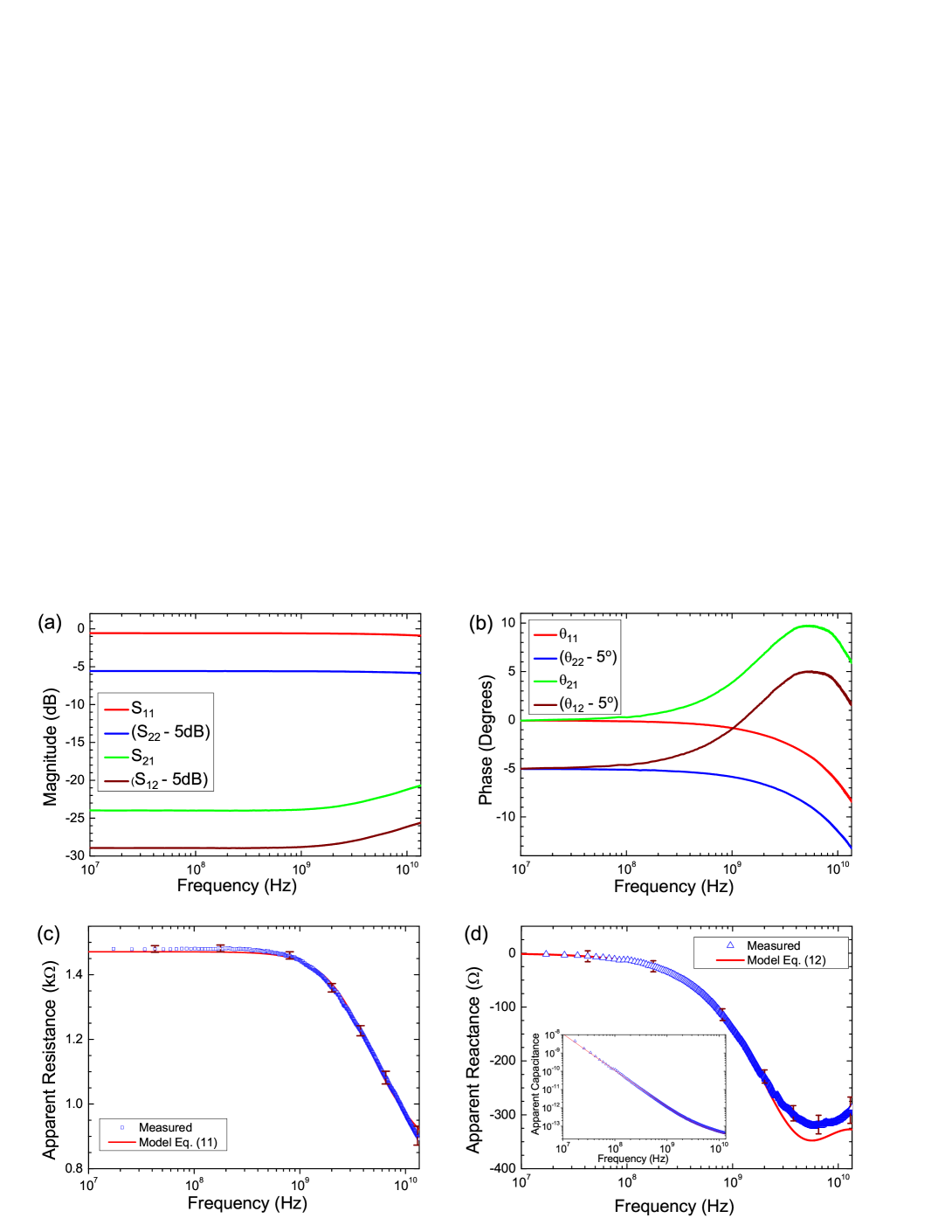
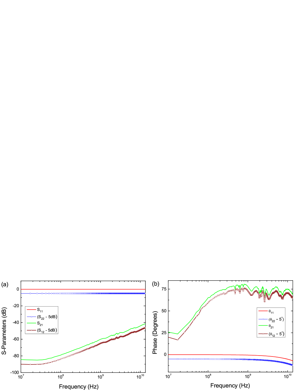
Fig.5 plots typical measured S-parameters magnitude and phase for an Open CPW device, and Fig.6 the corresponding ones for a Short CPW up to 13.5GHz. Using these data in Eq.(8), the admittance matrices of the Open and Short devices are determined and then inserted into Eq.(9) to derive the de-embedded intrinsic admittance matrix . The corresponding impedance matrix is determined using and the component of the intrinsic impedance of the GCPW is:
| (10) |
where and are the contact resistance and capacitance between SLG and the Cr/Au contacts and and are the SLG channel resistance and capacitance. The corresponding real and imaginary components of the impedance in Eq.(10) are given by:
| (11) |
and
| (12) |
where and are the apparent resistance and reactance of the GCPW, respectively. The second part of Eqs.(11, 12) resembles the Drude model even though the physical origin of the frequency dependence is different. In the electrical lumped-parameter RC model the frequency dependence arises due to the finite time required to charge/discharge a capacitor shunted by a resistance. In the Drude model, the origin of the frequency dependence is due to electron scattering with impurities, defects, etc. having a characteristic exponential relaxation time constant (which can range from 0.01-2 ps depending on the SLG mobility, Fermi level and velocityLinQE20 ; DasRMP83 ; TseAPL93 ). The Drude model for SLG suggests that for low frequencies the real part of the conductivity is approximately identical to the DC conductivity, with , whereas at higher frequencies and . Identical dependencies also emerge for the case of a SLG channel represented as a RC network with time constant , as shown in the second part of Eqs.(11, 12). However, in the latter case the frequency dependence arises due to .
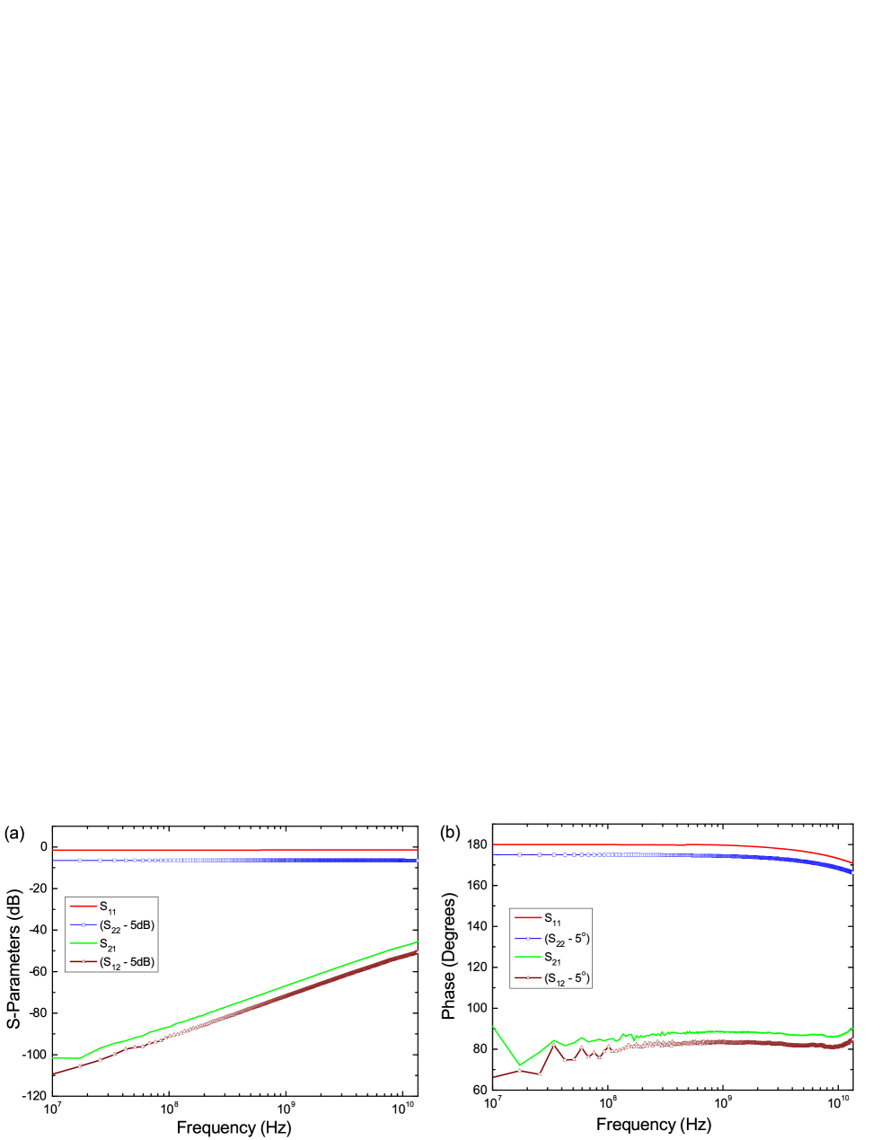
Fig.7 shows typical S-parameter measurements of our Au Thru devices and the extracted transmission line parameters, resistance (R), inductance (L), conductance (B) and capacitance (C), using Eq.(6). The transmission and reflection parameters demonstrate a small power dissipation in the Thru device up to 13.5GHz, with incident power . This remains constant up to 7GHz, then increases slightly to at higher frequencies, due to Eddy current losses in the metallic conductorsAwanBOOK ; DuffBOOK . In contrast, the inductance and capacitance have frequency-independent response up to 13.5GHz, as expected, whereas the conductance has only a slight dependence, due to substrate losses.
Fig.8 plots the measured scattering parameters, apparent resistance and reactance , and their calculated values based on Eqs.(11,12), for our GCPW at frequencies up to 13.5GHz at room temperature (at 0dBm and with in Fig.4). In contrast with the Au Thru device, the and parameters show RF and microwave transmission to be less than -20dB (or 100mV/V) at frequencies up to 13.5GHz, due to impedance mismatch with the measurement system, as expected based on the DC 2-probe resistance measurements. This level of transmission is found to be sufficient, combined with the calibration of the measurement system and employing parasitic impedance de-embedding, to extract the intrinsic electromagnetic properties of the SLG channel. A comparison of the power transmission, reflection and absorption coefficients of our GCPW with the Au Thru waveguide is shown in Table 1. For , of the RF and microwave power is reflected, whilst 0.4% is transmitted through the SLG channel and 12% is absorbed (similar to the reference Thru device simulated and measured in Figs.1,7). In contrast, at 13.5GHz the reflected power reduces to and transmitted power increases to 0.9%, whereas the absorbed power increases to.
| • | Au-Thru | Au-Thru | GCPW | GCPW |
|---|---|---|---|---|
| • | ||||
| Transmission | 83.6% | 82.6% | 0.4% | 0.9% |
| Reflection | 0.7% | 0.8% | 87.6% | 81.3% |
| Absorption | 15.7% | 16.6% | 12% | 17.8% |
| • | ||||||
|---|---|---|---|---|---|---|
| GCPW #1 | 28.9 | 891 | 2.4 | 289 | 0.12 | 2.1 |
| GCPW #2 | 34.1 | 760 | 2.1 | 292 | 0.15 | 1.6 |
A least-squares fit to the measured apparent resistance and reactance in Fig.8 gives /contact and /contact, with , and . For is constant with frequency, and its measured magnitude is , in close agreement with the 2-probe DC value of . Thus, the intrinsic DC conductivity of our SLG channel is after removal of the contact resistance. For , rapidly decreases to at 13.5GHz, indicative of the presence of contact capacitance and resistance in the waveguide device (represented by the first part of Eq.(11)). We get and , with equivalent to a 4-probe resistance extracted from a 2-probe measurement. This extraction of 4-probe resistance from a 2-probe measurement, deploying our RF and microwave method, could also be useful for other applications where an independent method is needed for comparison with standard DC 4-probe measurements. Furthermore, when devices are inherently 2-probe, our RF and microwave method could extract their intrinsic 4-probe properties.
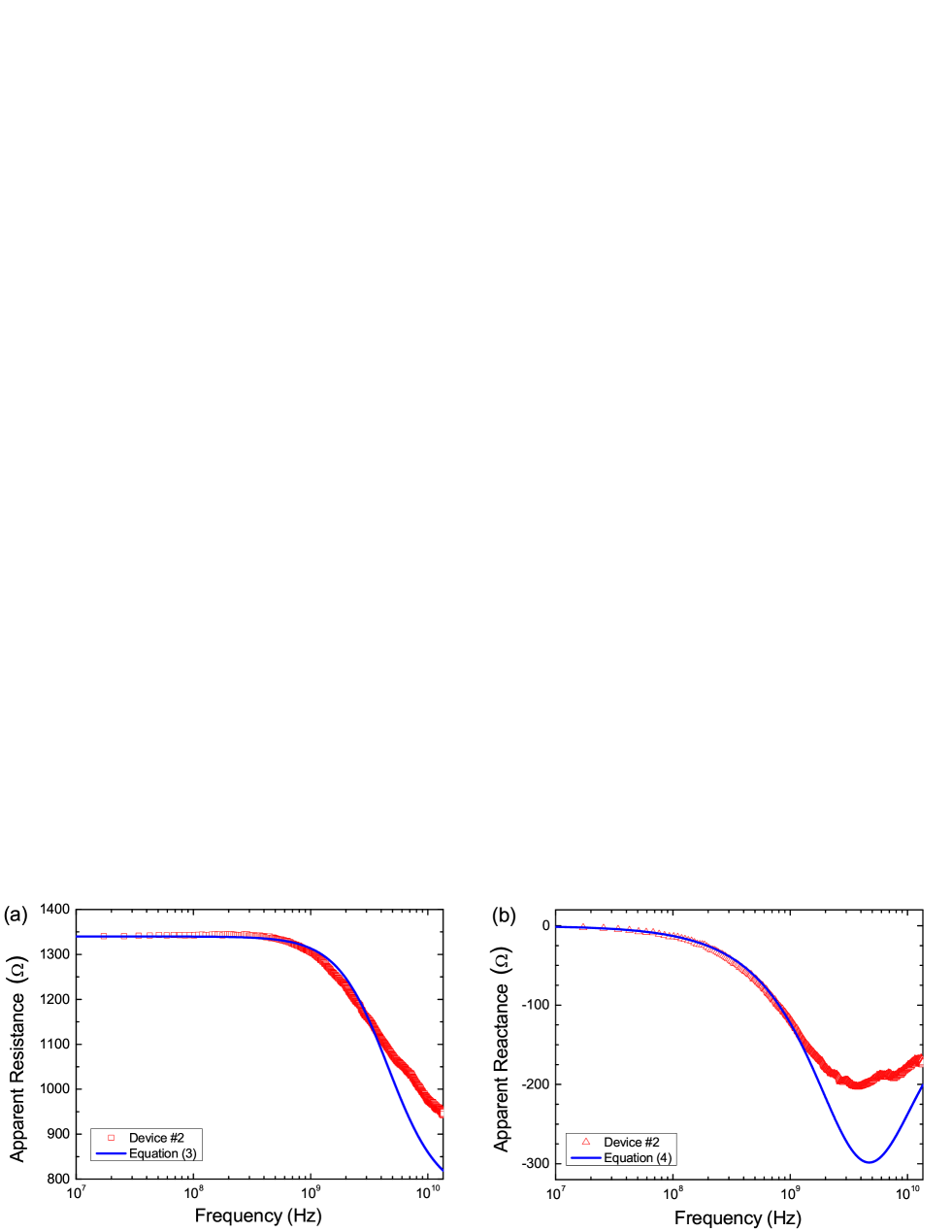
The measured up to 13.5GHz, given in Fig.8, shows good agreement with Eq.12, to within 2.7 uncertainty for reactance measurements. The measured and calculated show a minima at6GHz, due to the presence of , as for Fig.1(b). The inset in Fig.8 shows converted to an apparent capacitance. Fig.9 plots the measured apparent resistance and reactance of a second GCPW device at 0dBm and 0V back-gate. We get . Also shown for comparison is the calculated response based on the model of Fig.1 and Eqs.(11,12). Reasonably good qualitative agreement is observed between the data in Figs.8 and 9. The corresponding extracted device parameters are given in Table II. The extracted for the two GCPW devices, and 2.1fF, are compatible to the estimateYuPNAS110 using . The quantum capacitanceYuPNAS110 is found to be , where the density of states and is the spin and valley degeneracy. The total capacitance is the series combination of the geometric and quantum capacitance given by and is close to the geometric capacitance, since .
The time constants for the two devices are and , respectively, (which compare well with reported in Ref.[LiN4, ]). The former leads to at 13.5GHz (from the second part in Eq.(11)). However, and the corresponding real components of the conductivity and for the two GCPW devices, are found to be frequency-independent up to 13.5GHz, since is the same for the entire 0.01 to 13.5GHz range. Thus, the intrinsic electromagnetic response of SLG when carrying RF and microwave signals does not involve any additional power dissipation with respect to that at DC (i.e. Joule heating) up to 13.5GHz within our experimental uncertainty of 1.6. These results also suggest that the background of absorption in the single-particle optical gap is very small, in agreement with recent reports WoesNM14 . This background, not captured by the single-particle (Drude) model considered here, is due to electron-electron interactions PrinPRB88 and vanishes at increasing following a relation PrinPRB88 .
Static and dynamic conductivities are found to be identical, i.e. up to 13.5GHz. This represents a unique property of graphene in comparison with other materials, such as metalsPoza ; DuffBOOK and superconductorsAwanIPSMT149 , when carrying transport RF and microwave signals. This may have significant impact on the future design of ultra high-speed electronic devices based on graphene (potentially up to THz based on extrapolation of the models and their agreement with our results reported here, albeit to 13.5GHz), as well as their eventual very large scale integration (VLSI) into integrated circuits, particularly in comparison with the high dissipation (100Wcm-2) typically found in current state-of-the-art interconnects and Si based processors operating at few GHzBakerRJ .
III Conclusions
We reported the room-temperature transport conductivity of graphene at frequencies up to 13.5GHz measured using coplanar waveguides. This is independent of the frequency of the applied transport current in the DC to microwave range, so that the real and imaginary components of the complex AC dynamic conductivity are and , suggesting negligible additional power dissipation at high-frequencies compared to DC. Our results are in good agreement with the Drude model for dynamic conductivity with a momentum relaxation time and , for the two measured devices. This contrasts the quadratic frequency-dependence usually found in metals and superconductors and is promising for the future potential applications of graphene in ultra high-speed electronic devices. In particular, the measured frequency-independent resistance suggests it may be possible to realize broadband and low noise radiation detectors, high-frequency low noise amplifiers and mixers. We also anticipate potential applications in a variety of radio-frequency and microwave sensors enabling spectroscopic detection of physical or biological properties of materials and substances (i.e. in the case of biosensors antibody-antigen interactions at the graphene surface), in contrast with existing static conductance change based sensors.
IV Acknowledgements
We acknowledge funding from EU Graphene Flagship (no. 604391), ERC Grant Hetero2D, EPSRC Grants EP/K01711X/1, EP/K017144/1, RR/105758, Wolfson College, a Royal Society Wolfson Research Merit Award and M. Polini, A. Awan, B. Kibble, I. Robinson, N. Ridler, G. Pan, P. Davey, M. Z. Ahmed, L. Garcia-Gancedo, A. Katsounaros, M. Luukkainen, S. Ellilä, G. Fisher, S. Wordingham and C. Barnett for useful discussions.
References
- (1) Novoselov K S, Geim A K, Morozov S V, Jiang D, Zhang Y, Dubonos S V, Grigorieva I V and Firsov A A 2004 Science 306 666-669
- (2) Ferrari A C , et al. Nanoscale 7 4587-5062
- (3) Vicarelli L, Vitiello M S, Coquillat D. Lombardo A, Ferrari A C, Knap W, Polini M, Pellegrini V and Tredicucci A 2012 Nature Materials 11 865-871
- (4) Spirito D, Coquillat D, De Bonis S L, Lombardo A, Bruna M, Ferrari A C, Pellegrini V, Tredicucci A, Knap W and Vitiello M S 2014 Appl. Phys. Lett. 061111
- (5) Sordan R and Ferrari A C 2013 IEEE Int. Electron Devices Meeting 1-7
- (6) Novoselov K S, Geim A K, Morozov S V, Jiang D, Katsnelson M I, Grigorieva I V, Dubonos S V and Firsov A A 2005 Nature 438 197-200
- (7) Wu Y, Lin Y-M, Bol A A, Jenkins K A, Xia F, Farmer D B, Zhu Y and Avouris P 2011 Nature 472 74-78
- (8) Wu Y, Jenkins K A, Valdes-Garcia A, Farmer D B, Zhu Y, Bol A A, Dimitrakopoulos C, Zhu W, Xia F, Avouris P and Lin Y-M 2012 Nano Letters 12 3062-3067
- (9) Liao L, Lin Y-C, Bao M, Cheng R, Bai J, Liu Y, Qu Y, Wang K L, Huang Y and Duan X 2010 Nature 467 305-308
- (10) Lin Y-M, Jenkins K A, Valdes-Garcia A, Small J P, Farmer D B and Avouris P 2009 Nano Letters 9 422-426
- (11) Lin Y-M, Dimitrakopoulos C, Jenkins K A, Farmer D B, Chiu H-Y, Grill A, Avouris P 2010 Science 327 662-662
- (12) Pallecchi E, Benz C, Betz A C, Lo¨hneysen H v, Placais B and Danneau R 2011 Appl. Phys. Lett. 99 113502
- (13) Moon J S, Curtis D, Hu M, Wong D, McGuire C, Campbell P M, Jernigan G, Tedesco J L, VanMil B, Myers-Ward R, Eddy Jr C and Gaskill D K 2009 IEEE Electron Dev. Lett. 30 650-652
- (14) Lemme M C, Echtermeyer T J, Baus M and Kurz H 2007 IEEE Electron Dev. Lett. 28 282-284
- (15) Das S and Appenzeller J 2011 J. Proc. IEEE RFIC 1-4
- (16) Wang H, Hsu A, Wu J, Kong J and Palacios T 2010 IEEE Electron Dev. Lett. 31 906-908
- (17) Yang X B, Liu G X, Balandin A A and Mohanram K 2010 ACS Nano 4 5532-5538
- (18) Dragoman M, Muller A A, Dragoman D, Coccetti F and Plana R 2010 Journal of Applied Physics 107 104313
- (19) Mayorov A S, Gorbachev R V, Morozov S V, Britnell L, Jalil R, Ponomareko L A, Blake P, Novoselov K S, Watanabe K, Taniguchi T and Geim A K 2011 Nano Lett. 11, 2396-2399
- (20) Yu J, Liu G, Sumant A V, Goyal V and Balandin A A 2012 Nano Letters 12, 1603-1608
- (21) Balandin A A, Ghosh S, Bao W, Calizo I, Teweldebrhan D, Miao F and Lau C N 2008 Nano Letters 8, 902-907
- (22) Bertozzi D and Benini L 2004 IEEE Circuits Systems Magazine, 18-31
- (23) Deal W R 2008 IEEE Microwave Magazine 9, 120
- (24) Ando T, Zheng Y and Suzuura H 2002 J. Phys. Soc. Jpn. 71, 1318-1324
- (25) Hanson G W 2008 J. Appl. Phys. 103, 064302
- (26) Gusynin V P, Sharapov S G and Carbotte J P 2007 J. Phys. : Condens. Matt. 19, 026222
- (27) Kubo R 1957 J. Phys. Soc. Jpn. 12, 570-586
- (28) Koshino M and Ando T, 2009 Solid State Commun. 149, 1123-1127
- (29) Koshino, M and McCann E 2013 Phys. Rev. B 87 045420
- (30) Horng J, Chen C-F, Geng B , Girit C , Zhang Y, Hao Z, Bechtel H A, Martin M, Zettl A, Crommie M F, Shen Y R and Wang F 2011 Physical Review B 83 165113
- (31) Abedinpour S H, Vignale G, Principi A, Polini M, Tse W K and MacDonald A H 2011 Physical Review B 84 045429
- (32) Falkovsky L A, Varlamov A A 2007 Eur. Phys. J. B 56 281
- (33) Koppens F H L, Chang D E and de Abajo F J G 2011 Nano Letters 11 3370
- (34) Kittel C 2005 Introduction To Solid State Physics (John Wiley and Sons) ISBN: 978-0-471-41526-8
- (35) Tan Y-W, Zhang Y, Bolotin K, Zhao Y, Adam S, Hwang E H, Das Sarma S, Stormer H L, and Kim P 2007 Physical Review Letters 99 246803
- (36) Mittendor M, Wendler F, Malic E, Knorr A, Orlita Milan, Potemski M, Berger C, de Heer W A, Schneider H, Helm M, and Winnerl S 2015 Nature Physics 11 75-81
- (37) Lin I-T and Liu J-M 2014 IEEE Quant. Electron. 20 8400108
- (38) Wen C P 1969 IEEE Trans. Microwave Theory Tech. 17 1087-1090
- (39) Pozar D M 2005 Microwave Engineering, 3rd Edition (Intl. Ed.); John Wiley & Sons, Inc.; ISBN 0-471-44878-8
- (40) Marks R B A 1991 IEEE Trans. Microwave Theory Tech. 39 1205-1215
- (41) Moon S, Jung K, Park K, Kim H , Lee C-W, Baik C-W and Kim J M 2010 New Journal of Physics 12 113031
- (42) Lee H J, Kim E, Yook J G and Jung J 2012 Appl. Phys. Lett. 100 223102
- (43) Skulason H S, Nguyen H V, Guermoune A, Sridharan V, Siaj M, Caloz C and Szkopek T 2011 Appl. Phys. Lett. 99 153504
- (44) Novoselov K S, Jiang D, Schedin F, Booth T J, Khotkevich V V, Morozov S V and Geim A K 2005 PNAS, 102, 10451-10453
- (45) Jeckelmann B and Jeanneret B 2001 Reports on Progress in Physics 64, 1603-1655
- (46) Plombon J J, O’Brien K P, Gstrein F, Dubin V M and Jiao Y 2007 Appl. Phys. Lett. 90 063106
- (47) Yang Y, Tan C Y, Sun W Q, Li W, Ong C K, Liu Y, Li Y and Xu S Y 2011 Appl. Phys. Lett. 98 093107
- (48) Awan S A and Sali S 2002 IEE Proc. Sci. Meas. Technol. 149 2-8
- (49) Rutherglen C, Jain D and Burke P 2009 Nature Nanotechnology 4, 811-819
- (50) Rouhi N, Capdevila S, Jain D, Zand K, WangY Y, Brown E, Jofre L and Burke P 2012 Nano Res. 5 667-678
- (51) Mikhailov S A and Ziegler K Physical Review Letters 99 016803
- (52) Casiraghi C, Hartschuh A, Lidorikis E, Qian H, Harutyunyan H, Gokus T Novoselov K S and Ferrari A C 2007 Nano Letters 7 2711-2717
- (53) Ferrari A C, Meyer J C, Scardaci V, Casiraghi C, Lazzeri M, Mauri F, Piscanec S, Jiang D, Novoselov K S, Roth S and Geim A K 2006 Physical Review Letters 97 187401
- (54) Ferrari A C and Basko D M 2013Nature Nanotech. 8 235-246
- (55) Bonaccorso F, Lombardo A, Hasan T, Sun Z, Colombo L and Ferrari1 A C 2012 Materials Today 15 564-589
- (56) Pisana S, Lazzeri M, Casiraghi C, Novoselov K S,Geim A K, Ferrari A C and Mauri F 2007 Nature Materials 6 198-201
- (57) Basko D M, Piscanec S and Ferrari A C 2009 Physical Review B 80 165413
- (58) Das A, Pisana S, Chakraborty B, Piscanec S, Saha S K, Waghmare U V, Novoselov K S, Krishnamurthy, Geim A K, Ferrari A C and Sood A K 2008 Nature Nanotechnology 3 210-215
- (59) Casiraghi C, Pisana S, Novoselov K S, Geim A K and Ferrari A C 2007 Appl. Phys. Lett. 91 233108
- (60) Awan S A, Kibble B P and Shürr J Coaxial electrical Circuits for interference-free measurements 2011 (Publisher IET) ISBN: 978-184-919-065-5
- (61) Duffin W J, 2001 (W.J. Duffin Publisher) ISBN : 978-095-104-381-3
- (62) Adam S, Hwang E H, Galitski V M and Das Sarma S 2007 PNAS 47, 18392-18397
- (63) Jargon J A, Marks R B and Rytting D K 1999 IEEE Trans.Microwave Theory Tech. 47 2008-2013
- (64) Nishimoto M Y, Hamai M, Laskar J and Lai R K 1994 IEEE Microwave and Guided Letts. 4 370-272
- (65) Imparato M, Weller T M and Dunleavy L 1999 IEEE Microwave Theory Tech. 4 1643-1646
- (66) Dambrine G, Cappy A, Heliodore F and Playez E 1988 IEEE Microwave Theory Tech. 36 1152-1159
- (67) Cho H J and Burk D E 1991 IEEE Trans. Electron Dev. 38 1371-1375
- (68) Lee S, Kim C S and Yu H K 2001 IEEE Trans. Electron Dev. 48 1374-1379
- (69) Das Sarma S, Adam S, Hwang E H and Rossi E 2011 Rev. Mod. Phys. 83 407-470
- (70) Tse W-K, Hwang E H and Das Sarma S 2008 Appl. Phys. Lett. 93, 023128
- (71) Yu G L, Jalil R, Belle B, Mayorov A S, Blake P, Schedin F, Morozov S V, Ponomarenko L A, Chiappini F, Wiedmann S, Zeitler U, Katsnelson M I, Geim A K Novoselov K S and Elias D C 2013 P. Natl. Acad. Sci. 110 3282-3286
- (72) Li Z Q, Henriksen E A, Jiang Z, Hao Z, Martin M C, Kim P, Stormer H L and Basov D N 2008 Nature 4 532-535
- (73) Woessner A, Lundeberg M B, Gao Y, Principi A, Alonso-Gonzaolez P, Carrega, M, Watanabe K, Taniguchi T, Vignale G, Polini M, Hone J, Hillenbrand R, Koppens F H L 2015 Nature Mat. 14, 421-425
- (74) Principi A, Vignale G, Carrega M and Polini M 2013 Physical Review B 88, 195405
- (75) Baker R J 2010 (Wiley-IEEE) ISBN : 978-0-470-88132-3