Unconventional spin texture in a non-centrosymmetric quantum spin Hall insulator
Abstract
We proposed that the simultaneous presence of both Rashba and band inversion can lead to a Rashba-like spin-splitting formed by two bands with the same in-plane helical spin texture. Because of this unconventional spin texture, the backscattering is forbidden in edge and bulk conductivity channels. We propose a new non-centrosymmetric honeycomb-lattice quantum spin Hall (QSH) insulator family formed by the IV, V, and VII elements with this property. The system formed by Bi, Pb and I atoms is mechanically stable and has both a large Rashba spin-splitting of 60 meV and a large nontrivial band gap of 0.14 eV. Since the edge and the bulk states are protected by the TR symmetry, contrary to what happens in most doped QSH insulators, the bulk states do not contribute to the backscattering in the electronic transport, allowing the construction of a spintronic device with less energy loss.
pacs:
71.70.Ej, 72.20.-i, 72.25.Dc, 31.15.A-The main objective of spintronics is to understand the mechanisms by which it is possible to achieve efficient control of both spin configurations and spin currentsPesin and MacDonald (2012); Žutić et al. (2004). In the last decade, the way to achieve this objective has experienced a breakthrough due to i) the discovery and understanding of mechanisms to generate spin currents in conductors with magnetic order and in paramagnetic conductors/semiconductorsBrataas et al. (2012); Liang et al. (2015); Liu et al. (2012), ii) the experimental observation of theoretically proposed spin injector systemsHasan and Kane (2010); Qi and Zhang (2011); Brune et al. (2012), and iii) the synthesis of 2D materials with long spin relaxation timePesin and MacDonald (2012); Kulik et al. (2015). The generation of spin currents, spin injections and spin conservation are mediated by the spin-orbit coupling (SOC) mainly via Rashba effect and/or nontrivial topological phasesMaekawa et al. (2012); Jansen (2012); Manchon et al. (2015); Bercioux and Lucignano (2015), such as the quantum spin Hall (QSH) effectKane and Mele (2005). Therefore, the search for systems experiencing these properties is a primary concern for the development of spintronics.
QSH insulators support helical metallic edge states, forming topological Dirac fermions protected by the time-reversal (TR) symmetry on an insulating bulkHasan and Kane (2010); Qi and Zhang (2011). The topological transition from trivial insulating to topological insulators is evidenced as a band inversion at the TR invariant -point mediated by the SOC. The topological band dispersion has been experimentally characterized via angle-resolved photoemission spectroscopy (ARPES) and local scanning tunneling microscopy (STM) in 3D topological insulatorsHasan and Kane (2010), and via transport measurements in HgTe/CdTe quantum wellsKönig et al. (2007); Olshanetsky et al. (2015). On the other hand, the Rashba effect, arising from the lack of inversion symmetry, leads to parallel spin-polarized band dispersion curves with opposite in-plane chiral spin textureBychkov and Rashba (1984), allowing the control of the spin direction through an electric fieldMaekawa et al. (2012); Manchon et al. (2015); Bercioux and Lucignano (2015). These dispersion curves and Fermi contours have been characterized by spectroscopic measurements for many surfaces and interfacesLaShell et al. (1996); Ast et al. (2007); Koroteev et al. (2004); Nitta et al. (1997). Large Rashba spin-splitting are found in materials formed by heavy elements with strong intrinsic SOC such as Bi, Pb, W, among othersHirahara et al. (2006); Mathias et al. (2010); Nitta et al. (1997); Yuan et al. (2013); Dil et al. (2008). In this work, we look at the consequences of the simultaneous presence of a Rashba spin-splitting and a inverted bandgap. Such properties appear simultaneously in thin films and heterostructures of 3D topological insulatorsZhu et al. (2011); Zhang et al. (2010); Ishizaka et al. (2011); Bahramy et al. (2012); Das and Balatsky (2013); Zhou et al. (2014).
Here, we show that bulk states can be protected against backscattering in nanoribbons of QSH insulators with bulk inversion asymmetry. This behavior is a consequence of the simultaneous presence of both Rashba and band inversion in a QSH insulator. In our model, both the conduction and the valence bands are formed by two bands with the same in-plane helical spin texture and opposite spin component. We propose a stable non-centrosymmetric honeycomb-lattice QSH insulator that presents this unconventional bulk spin texture. This system is formed by the Bi, Pb, and I elements and, has a large nontrivial band gap of eV and a huge Rashba spin-splitting of meV. To construct the Hamiltonian exhibiting the proposed spin texture we will use the PbBiI system.
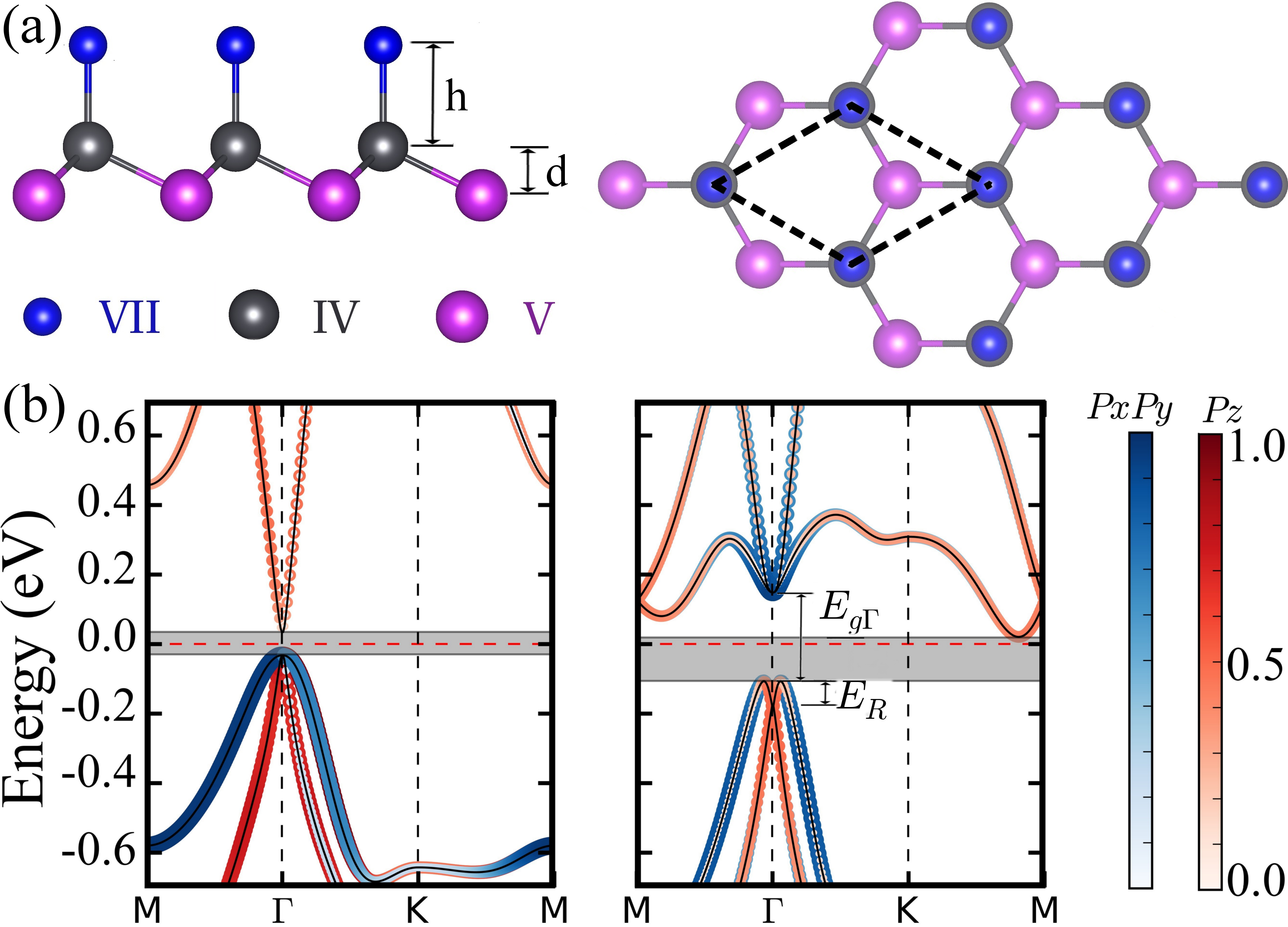
Figure 1 summarizes the crystalline structure and the results we obtain from ab initio calculations, which are performed within the density functional theory (DFT) framework as implemented in the SIESTA codeSoler et al. (2002) and in the Vienna Ab Initio Simulation PackageKresse and Furthmüller (1996). We consider the on-site approximation for the SOCAcosta et al. (2014); Fernandez-Seivane et al. (2006) in the SIESTA code. The Local Density ApproximationPerdew and Zunger (1981) and the Perdew-Burke-Ernzenhof generalized gradient approximationPerdew et al. (1996) are used for the exchange-correlation functional. Interpreting the hexagonal lattice as two triangular sub-lattices A and B, the system has a V atom type on the sub-lattice A, and a IV-VII dimer in the sub-lattice B (Fig 1a). These non-centrosymmetry systems have a buckled format and fulfill the symmetry operations of the symmetry: i) three-fold rotation symmetry along the axis, ii) mirror symmetry () in the plane, and iv) TR symmetry . We predict that the PbBiI system is mechanically stable, imaginary frequencies does not exist in the ab initio phonon spectrum (see Supplemental Material) and the formation energy () is about eV.
At the point, the top of the valence band is dominated by the Bi orbitals and the bottom of the conduction band mainly consists of the Bi orbitals, as shown in Fig 1b. When the SOC is taken into account, the orbitals are mixed to form effective orbitals preserving the total angular momentum and a band inversion occurs when , where means the absence (full presence) of SOC. We implemented the evolution of Wannier center of charges as an alternative method to the invariant calculation using ab-inito simulations Yu et al. (2011); Soluyanov and Vanderbilt (2011a, b). We find that there is no a horizontal reference line that crosses the evolution of the WCCs at least an odd number of times (see Supplemental Material), showing a value of Yu et al. (2011); Soluyanov and Vanderbilt (2011b), and hence, confirming that the PbBiI system is a QSH insulator. On the other hand, according to the symmetry operation, the wavefunction at the point is given by the effective states, where is the total angular momentum, is the projection along the axes, and corresponds to the Bi and Pb-I contributions. To preserve the total angular momentum, the effective states should be a linear combination of the and effective orbitals and, the effective states should be a linear combination of the orbitals, mainly orbitals. In this inverted band gap the conduction band mainly consists of Bi orbitals and the valence band is formed by the orbitals, mainly dominated by Bi orbitals, as shown in Fig 1b. Therefore, at the point, the valence (conduction) band is described by the effective states with () and hence, we write the Hamiltonian using the full SOC basis .
The tight-binding Hamiltonian matrix elements are given by:
| (1) |
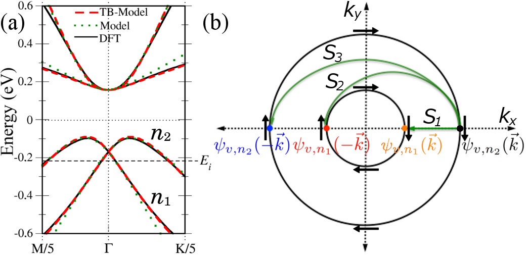
where , and is the on-site energy. Since the effective states contribution is not relevant near the Fermi energy, we omit the terms associated with the nearest neighbors (Pb-I dimer) and hence, represents the next nearest neighbor hopping terms, with indicating the lattice site and corresponding to the -th of the six next nearest neighbor vectors. Different form buckled honeycomb lattice systems, such as Germanene, Silicene among others, in which the nearest neighbor hopping terms are essential to its description, in the PbBiI the Pb-I dimer only mediates the interaction between Bi atoms and its effect is effectively introduced within the next nearest neighbor hopping terms. Therefore, the PbBiI Hamiltonian is striking different from the Kane-Mele modelKane and Mele (2005). Using the relevant symmetry operations of the point group, these hopping terms can be related to each other and are uniquely determined (see Supplemental Material), which leads to an approximate description of the DFT band structure (see Fig 2a).
Considering the limit we obtain a reduced form for the tight-binding Hamiltonian matrix elements,
| (2) |
where , , and . Here, and are the effective terms that described the and states, respectively and is the interaction between these states. The parameters are related to the hopping terms and are obtained via a least squares standard approach in order to match the DFT calculation (see Supplemental Material). Since we find that and considering , we rewrite the Hamiltonian as
| (3) |
We plot the Fermi contours obtained from this Hamiltonian and represent the backscattering processes in Fig 2b. In the valence band, an energy plane below(above) the band crossing consists of two concentric circles with the same(opposite) in-plane helical spin texture. Likewise, in the conduction band, an energy plane consists of two concentric circles with the same in-plane helical spin texture. Because of this bulk spin texture, the elastic and inelastic backscattering processes represented by and , respectively, are forbidden.
In order to quantify the probability of backscattering, we calculate the scattering rate due to a single coulomb impurity considering the bare coulomb potentialYin et al. (2014), . Here, is the unit area, is the single-electron charge, is the static dielectric constant and and is the overlap integral, which is calculated using the normalized wavefunction,
| (4) |
where . We verify that and therefore the scattering rates and are null, proving that backscattering processes are unlikely. On the other hand, in an ordinary out-plane spin polarized Rashba material, such as the thin films of the BiTeI 3D topological insulatorIshizaka et al. (2011), in an energy plane below(above) the band crossing the bands have opposite(same) in-plane chiral spin texture (Fig 3a) and therefore, the elastic backscattering is forbidden. Different from PbBiI, in a Rashba semiconductor, below the band crossing the inelastic backscattering is allowed and Bychkov and Rashba (1984); Sakamoto et al. (2013), as represented by the green arrows in Fig 3a.
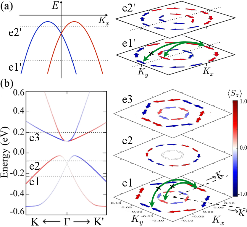
Far from the point, the symmetry breaking generates nonlinear terms in the SOC such as the three order Rashba term , which induces spin polarization and hexagonal warping effect in the bulk statesVajna et al. (2012); Fu (2009), as represented in Fig 3b. Although spin-polarized increases, the expected value of is still near zero. Because the and spin flips are required so that the inelastic scattering process occurs (see Fig 3b), the overlap integral is still small compared to the value found in an ordinary Rashba semiconductors and the probability that the scattering process occurs remains low. Analogous to the surface states of Bi2Te3Fu (2009), near the point, the spin-polarization and the warping hexagonal tend to zero and the only contribution coming from the lack of inversion symmetry is the first order Rashba term, . Thus, to obtain the unconventional spin texture near the point is only enough to consider both Rashba effect and band inversion, as it was done in eq. 3. According to our DFT results, the Rashba spin-splitting is about meV, which are huge compared with the values found in semiconductors and surprisingly is among the highest found in 3D systemsHirahara et al. (2006); Mathias et al. (2010); Nitta et al. (1997); Yuan et al. (2013); Dil et al. (2008); Ishizaka et al. (2011). This value can be increased up to meV applying large compressive strain (see Supplemental Material).
On the other hand, since the out-plane spin polarization oscillates according to the symmetry, as occurs in thin films of Bi2Te3Fu (2009), at the symmetry path, the spin component is zero (see Fig 3) and therefore, inelastic backscattering processes are completely suppressed. The armchair nanoribbon BZ is parallel to the symmetry path at the axis of the hexagonal BZ. Thus, scattering processes are dominated by the spin component and hence, the elastic and inelastic backscattering is forbidden for bulk and edge states, as shown in Fig 4. Similarly, the zigzag nanoribbon BZ is parallel to the axis and therefore, . Because of the non-zero spin components, there is a low probability of inelastic backscattering in accordance with the bulk behavior discussed above (see Supplemental Material). Because of the strong SOC, the spin and momentum are constrained to be perpendicular. This spin-momentum locking implies that Dirac cones of different edges are required to have the same spin texture and different spin texture of spin in the armchair nanoribbon, as represented in Fig 4c.
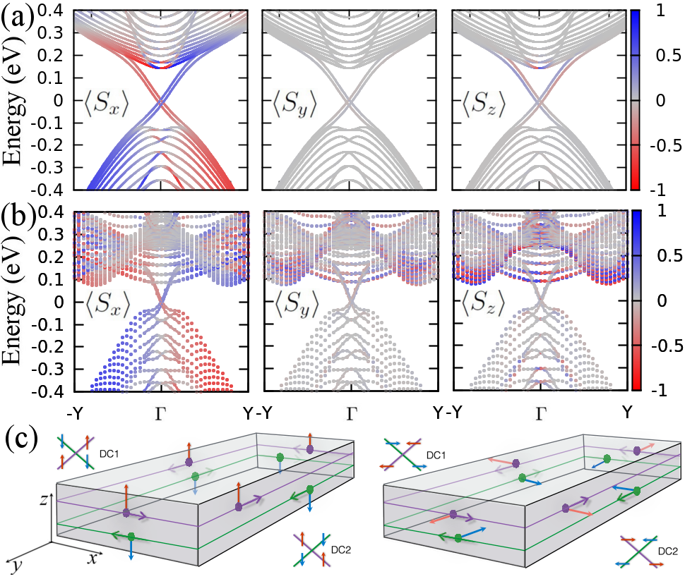
The protected bulk states near the point only appear in the energy region in which the Rashba effect and the band inversion point take place. This energy region overlaps with the bottom of the conduction band, which is at symmetry path, as shown inf Fig 4b. The bottom of the conduction band and hence, the energy range in which the unusual spin texture is present can be modified by applying tensile strain (see Supplemental Material). Indeed, the inverted bandgap at can be equal to the bandgap when strain is applied.
It is well established that the Bi-Pb alloy can be realized experimentally maintaining the space group Gokcen (1992); Huang and Serrano (1983). The Pb-Bi rhombohedral alloy along the [111] direction can be considered as a stack of PbBi honeycomb lattices that are weakly bonded (mainly ruled by Van der Waals type interaction) to each other, similarly to the bismuth bilayersDrozdov et al. (2014). The dangling bonds that appear at the Pb-rich PbBi surface can be eliminated by bonding to iodine atoms and hence, the proposed spin texture could be observed in the PbBiI system via STM experiments analogously to the observation of Bi-bilayers’ edge statesDrozdov et al. (2014).
The symmetry in the PbBiI system leads to a interaction term different from the BHZ model used to describe the QHS phase in HgTe/CdTe quantum wellsBernevig et al. (2006). Although the BHZ model considering the Rashba effect has been used to describe asymmetric InAs/GaSb/AlSb quantum wellsLiu et al. (2008), the consequences of a huge Rashba spin-splitting and the three order Rashba term in a bulk inverted band gap, such as the unconventional spin texture reported here, have been ignored.
In summarizing, the simultaneous presence of a huge Rashba effect and a inverted bandgap in systems with symmetry leads to conduction and valence bands with a Rashba-like spin-splitting with the same helical in-plane spin texture and with null spin-polarization at the symmetry paths. Thus, the spin texture in the nanoribbons depends on its orientation. We find that bulk states are protected by the TR symmetry and contrary to what happens in most doped QSH systems, the bulk states do not contribute to the backscattering, opening the way for realizing novel applications of topological edge states. Additionally, we proposed a new honeycomb-lattice QSH insulator mechanically stable - the PbBiI system, which has a large Rashba splitting of 60 meV, a large nontrivial gap of 0.14 eV and hence, it presents the predicted unconventional spin texture. As far as we know, the PbBiI system is the first system that has such spin texture properties in its bulk band structure.
Acknowledgements.
This work was supported by the Sao Paulo research foundation (grant 2014/12357-3). We would like to thank Dr. Luis G. G. V. Dias da Silva by the discussions. We also acknowledge Dr. Soluyanov and Dr. Vanderbilt for sharing the code to calculate the WCCs with VASP.References
- Pesin and MacDonald (2012) D. Pesin and A. H. MacDonald, Nat Mater 11, 409 (2012).
- Žutić et al. (2004) I. Žutić, J. Fabian, and S. Das Sarma, Rev. Mod. Phys. 76, 323 (2004).
- Brataas et al. (2012) A. Brataas, A. D. Kent, and H. Ohno, Nat Mater 11, 372 (2012).
- Liang et al. (2015) T. Liang, Q. Gibson, M. N. Ali, M. Liu, R. J. Cava, and N. P. Ong, Nat Mater 14, 280 (2015), letter.
- Liu et al. (2012) L. Liu, O. J. Lee, T. J. Gudmundsen, D. C. Ralph, and R. A. Buhrman, Phys. Rev. Lett. 109, 096602 (2012).
- Hasan and Kane (2010) M. Z. Hasan and C. L. Kane, Rev. Mod. Phys. 82, 3045 (2010).
- Qi and Zhang (2011) X.-L. Qi and S.-C. Zhang, Rev. Mod. Phys. 83, 1057 (2011).
- Brune et al. (2012) C. Brune, A. Roth, H. Buhmann, E. M. Hankiewicz, L. W. Molenkamp, J. Maciejko, X.-L. Qi, and S.-C. Zhang, Nat Phys 8, 485 (2012).
- Kulik et al. (2015) L. V. Kulik, A. V. Gorbunov, A. S. Zhuravlev, V. B. Timofeev, S. Dickmann, and I. V. Kukushkin, Sci. Rep. 5 (2015), article.
- Maekawa et al. (2012) S. Maekawa, S. O. Valenzuela, E. Saitoh, and T. Kimura, Spin Current (Series on Semiconductor Science and Technology 17, Oxford University Pres, 2012).
- Jansen (2012) R. Jansen, Nat Mater 11, 400 (2012).
- Manchon et al. (2015) A. Manchon, H. C. Koo, J. Nitta, S. M. Frolov, and R. A. Duine, Nat Mater 14, 871 (2015).
- Bercioux and Lucignano (2015) D. Bercioux and P. Lucignano, Reports on Progress in Physics 78, 106001 (2015).
- Kane and Mele (2005) C. L. Kane and E. J. Mele, Phys. Rev. Lett. 95, 146802 (2005).
- König et al. (2007) M. König, S. Wiedmann, C. Brüne, A. Roth, H. Buhmann, L. W. Molenkamp, X.-L. Qi, and S.-C. Zhang, Science 318, 766 (2007).
- Olshanetsky et al. (2015) E. B. Olshanetsky, Z. D. Kvon, G. M. Gusev, A. D. Levin, O. E. Raichev, N. N. Mikhailov, and S. A. Dvoretsky, Phys. Rev. Lett. 114, 126802 (2015).
- Bychkov and Rashba (1984) Y. A. Bychkov and E. I. Rashba, JETP Lett 39, 78 (1984).
- LaShell et al. (1996) S. LaShell, B. A. McDougall, and E. Jensen, Phys. Rev. Lett. 77, 3419 (1996).
- Ast et al. (2007) C. R. Ast, J. Henk, A. Ernst, L. Moreschini, M. C. Falub, D. Pacilé, P. Bruno, K. Kern, and M. Grioni, Phys. Rev. Lett. 98, 186807 (2007).
- Koroteev et al. (2004) Y. M. Koroteev, G. Bihlmayer, J. E. Gayone, E. V. Chulkov, S. Blügel, P. M. Echenique, and P. Hofmann, Phys. Rev. Lett. 93, 046403 (2004).
- Nitta et al. (1997) J. Nitta, T. Akazaki, H. Takayanagi, and T. Enoki, Phys. Rev. Lett. 78, 1335 (1997).
- Hirahara et al. (2006) T. Hirahara, T. Nagao, I. Matsuda, G. Bihlmayer, E. V. Chulkov, Y. M. Koroteev, P. M. Echenique, M. Saito, and S. Hasegawa, Phys. Rev. Lett. 97, 146803 (2006).
- Mathias et al. (2010) S. Mathias, A. Ruffing, F. Deicke, M. Wiesenmayer, I. Sakar, G. Bihlmayer, E. V. Chulkov, Y. M. Koroteev, P. M. Echenique, M. Bauer, and M. Aeschlimann, Phys. Rev. Lett. 104, 066802 (2010).
- Yuan et al. (2013) H. Yuan, M. S. Bahramy, K. Morimoto, S. Wu, K. Nomura, B.-J. Yang, H. Shimotani, R. Suzuki, M. Toh, C. Kloc, X. Xu, R. Arita, N. Nagaosa, and Y. Iwasa, Nat Phys 9, 563 (2013), article.
- Dil et al. (2008) J. H. Dil, F. Meier, J. Lobo-Checa, L. Patthey, G. Bihlmayer, and J. Osterwalder, Phys. Rev. Lett. 101, 266802 (2008).
- Zhu et al. (2011) Z.-H. Zhu, G. Levy, B. Ludbrook, C. N. Veenstra, J. A. Rosen, R. Comin, D. Wong, P. Dosanjh, A. Ubaldini, P. Syers, N. P. Butch, J. Paglione, I. S. Elfimov, and A. Damascelli, Phys. Rev. Lett. 107, 186405 (2011).
- Zhang et al. (2010) Y. Zhang, K. He, C.-Z. Chang, C.-L. Song, L.-L. Wang, X. Chen, J.-F. Jia, Z. Fang, X. Dai, W.-Y. Shan, S.-Q. Shen, Q. Niu, X.-L. Qi, S.-C. Zhang, X.-C. Ma, and Q.-K. Xue, Nat Phys 6, 584 (2010).
- Ishizaka et al. (2011) K. Ishizaka, M. S. Bahramy, H. Murakawa, M. Sakano, T. Shimojima, T. Sonobe, K. Koizumi, S. Shin, H. Miyahara, A. Kimura, K. Miyamoto, T. Okuda, H. Namatame, M. Taniguchi, R. Arita, N. Nagaosa, K. Kobayashi, Y. Murakami, R. Kumai, Y. Kaneko, Y. Onose, and Y. Tokura, Nat Mater 10, 521 (2011).
- Bahramy et al. (2012) M. S. Bahramy, B. J. Yang, R. Arita, and N. Nagaosa, Nat Commun 3, 679 (2012).
- Das and Balatsky (2013) T. Das and A. V. Balatsky, Nat Commun 4 (2013).
- Zhou et al. (2014) J.-J. Zhou, W. Feng, Y. Zhang, S. A. Yang, and Y. Yao, Scientific Reports 4, 3841 EP (2014).
- Soler et al. (2002) J. M. Soler, E. Artacho, J. D. Gale, A. García, J. Junquera, P. Ordejón, and D. Sánchez-Portal, Journal of Physics: Condensed Matter 14, 2745 (2002).
- Kresse and Furthmüller (1996) G. Kresse and J. Furthmüller, Phys. Rev. B 54, 11169 (1996).
- Acosta et al. (2014) C. M. Acosta, M. P. Lima, R. H. Miwa, A. J. R. da Silva, and A. Fazzio, Phys. Rev. B 89, 155438 (2014).
- Fernandez-Seivane et al. (2006) L. Fernandez-Seivane, M. A. Oliveira, S. Sanvito, and J. Ferrer, J. of Phys.: Condens. Matter 18, 7999 (2006).
- Perdew and Zunger (1981) J. P. Perdew and A. Zunger, Phys. Rev. B 23, 5048 (1981).
- Perdew et al. (1996) J. P. Perdew, K. Burke, and M. Ernzerhof, Phys. Rev. Lett. 77, 3865 (1996).
- Yu et al. (2011) R. Yu, X. L. Qi, A. Bernevig, Z. Fang, and X. Dai, Phys. Rev. B 84, 075119 (2011).
- Soluyanov and Vanderbilt (2011a) A. A. Soluyanov and D. Vanderbilt, Phys. Rev. B 83, 035108 (2011a).
- Soluyanov and Vanderbilt (2011b) A. A. Soluyanov and D. Vanderbilt, Phys. Rev. B 83, 235401 (2011b).
- Yin et al. (2014) G. Yin, D. Wickramaratne, Y. Zhao, and R. K. Lake, Applied Physics Letters 105, 033118 (2014).
- Sakamoto et al. (2013) K. Sakamoto, T.-H. Kim, T. Kuzumaki, B. Müller, Y. Yamamoto, M. Ohtaka, J. R. Osiecki, K. Miyamoto, Y. Takeichi, A. Harasawa, S. D. Stolwijk, A. B. Schmidt, J. Fujii, R. I. G. Uhrberg, M. Donath, H. W. Yeom, and T. Oda, Nat Commun 4 (2013).
- Vajna et al. (2012) S. Vajna, E. Simon, A. Szilva, K. Palotas, B. Ujfalussy, and L. Szunyogh, Phys. Rev. B 85, 075404 (2012).
- Fu (2009) L. Fu, Phys. Rev. Lett. 103, 266801 (2009).
- Gokcen (1992) N. Gokcen, Journal of Phase Equilibria 13, 21 (1992).
- Huang and Serrano (1983) H. C. W. Huang and C. M. Serrano, Journal of Vacuum Science and Technology A 1, 1409 (1983).
- Drozdov et al. (2014) I. K. Drozdov, A. Alexandradinata, S. Jeon, S. Nadj-Perge, H. Ji, R. J. Cava, B. Andrei Bernevig, and A. Yazdani, Nat Phys 10, 664 (2014).
- Bernevig et al. (2006) B. A. Bernevig, T. L. Hughes, and S.-C. Zhang, Science 314, 1757 (2006).
- Liu et al. (2008) C. Liu, T. L. Hughes, X.-L. Qi, K. Wang, and S.-C. Zhang, Phys. Rev. Lett. 100, 236601 (2008).