Impact of the slit geometry on the performance of wire-grid polarisers
Gwenaelle Mélen,1,∗ Wenjamin Rosenfeld1 and Harald Weinfurter1,2
1Ludwig-Maximilians-Universität, 80799 München, Germany
2Max-Planck-Institut für Quantenoptik, 85748 Garching, Germany
∗gwenaelle.vest@lmu.de
Abstract
Wire-grid polarisers are versatile and scalable components which can be engineered to achieve small sizes and extremely high extinction ratios. Yet the measured performances are always significantly below the predicted values obtained from numerical simulations. Here we report on a detailed comparison between theoretical and experimental performances. We show that the discrepancy can be explained by the true shape of the plasmonic structures. Taking into account the fabrication details, a new optimisation model enables us to achieve excellent agreement with the observed response and to re-optimise the grating parameters to ensure experimental extinction ratios well above 1,000 at 850 nm.
OCIS codes: (130.0130) Integrated optics; (220.0220) Optical design and fabrication; (050.0050) Diffraction and gratings; (230.5440) Polarisation-selective devices; (310.6628) Subwavelength structures, nanostructures.
References and links
- [1] G. R. Bird and M. Parrish, Jr., “The wire grid as a near-infrared polarizer,” J. Opt. Soc. Am. 50, 886 (1960).
- [2] S. Shishido, T. Noda, K. Sasagawa, T. Tokuda, and J. Ohta, “Polarization analyzing image sensor with on-chip metal wire grid polarizer in 65-nm standard complementary metal oxide semiconductor process,” Jpn. J. Appl. Phys. 50 (2011).
- [3] L. Wang, H. Schift, J. Gobrecht, Y. Ekinci, P. M. Kristiansen, H. H. Solak, and K. Jefimovs, “High-throughput fabrication of compact and flexible bilayer nanowire grid polarizers for deep-ultraviolet to infrared range,” J. Vac. Sci. Technol. B 32, 031206 (2014).
- [4] H. Lochbihler, “Surface polaritons on gold-wire gratings,” Phys. Rev. B 50, 4795–4801 (1994).
- [5] T. Thio, K. M. Pellerin, R. a. Linke, H. J. Lezec, and T. W. Ebbesen, “Enhanced light transmission through a single subwavelength aperture,” Opt. Lett. 26, 1972–1974 (2001).
- [6] S. Astilean, P. Lalanne, and M. Palamaru, “Light transmission through metallic channels much smaller than the wavelength,” Opt. Commun. 175, 265–273 (2000).
- [7] Y. Takakura, “Optical resonance in a narrow slit in a thick metallic screen,” Phys. Rev. Lett. 86, 5601–5603 (2001).
- [8] G. Vest, M. Rau, L. Fuchs, G. Corrielli, H. Weier, S. Nauerth, A. Crespi, R. Osellame, and H. Weinfurter, “Design and evaluation of a handheld quantum key distribution sender module,” IEEE J. Sel. Top. Quant. 21, 131–137 (2015).
- [9] S.-W. Ahn, K.-D. Lee, J.-S. Kim, S. H. Kim, J.-D. Park, S.-H. Lee, and P.-W. Yoon, “Fabrication of a 50 nm half-pitch wire grid polarizer using nanoimprint lithography,” Nanotechnology 16, 1874–1877 (2005).
- [10] J. S. Cetnar, J. R. Middendorf, and E. R. Brown, “Extraordinary optical transmission and extinction in a Terahertz wire-grid polarizer,” Appl. Phys. Lett. 100, 102–105 (2012).
- [11] Z. Y. Yang and Y. F. Lu, “Broadband nanowire-grid polarizers in ultraviolet-visible-near-infrared regions,” Opt. Express 15, 9510–9519 (2007).
- [12] T. Siefke, D. Lehr, T. Weber, D. Voigt, E.-B. Kley, and A. Tünnermann, “Fabrication influences on deep-ultraviolet tungsten wire grid polarizers manufactured by double patterning,” Opt. Lett. 39, 6434–6437 (2014).
- [13] X. Liu, X. Deng, P. Sciortino, M. Buonanno, F. Walters, R. Varghese, J. Bacon, L. Chen, N. O’Brien, and J. J. Wang, “Large area, 38 nm half-pitch grating fabrication by using atomic spacer lithography from aluminum wire grids,” Nano Lett. 6, 2723–2727 (2006).
- [14] J. H. Oh, D. H. Kang, W. H. Park, H. J. Kim, S. M. Hong, J. H. Hur, J. Jang, S. J. Lee, M. J. Kim, S. K. Kim, K. H. Park, E. Gardner, J. Hansen, M. Yost, and D. Hansen, “High-resolution stereoscopic TFT-LCD with wire grid polarizer,” SID Int. Symp. Dig. Tec. 38, 1164 (2007).
- [15] F. Marquier, J. Greffet, S. Collin, F. Pardo, and J. Pelouard, “Resonant transmission through a metallic film due to coupled modes,” Opt. Express 13, 70–76 (2005).
- [16] S. Collin, F. Pardo, and R. Teissier, “Horizontal and vertical surface resonances in transmission metallic gratings,” J. Opt. A - Pure Appl. Op. 4, 154–160 (2002).
- [17] M. Guillaumée, L. A. Dunbar, C. Santschi, E. Grenet, R. Eckert, O. J. F. Martin, and R. P. Stanley, “Polarization sensitive silicon photodiodes using nanostructured metallic grids,” Appl. Phys. Lett. 94, 193503 (2009).
- [18] A. F. Oskooi, D. Roundy, M. Ibanescu, P. Bermel, J. D. Joannopoulos, and S. G. Johnson, “MEEP: A flexible free-software package for electromagnetic simulations by the FDTD method,” Comput. Phys. Commun. 181, 687–702 (2010).
- [19] A. D. Rakic, A. B. Djurišic, J. M. Elazar, and M. L. Majewski, “Optical properties of metallic films for vertical-cavity optoelectronic devices,” Appl. Optics 37, 5271 (1998).
- [20] A. W. Snyder and J. D. Love, “Optical Waveguide Theory,” Chapman and Hall (1984).
- [21] H. F. Schouten, T. D. Visser, D. Lenstra, and H. Blok, “Light transmission through a subwavelength slit: waveguiding and optical vortices,” Phys. Rev. E 67, 036608 (2003).
- [22] H. Ryu, S. Joon Yoon, and D. Kim, “Influence of surface roughness on the polarimetric characteristics of a wire-grid grating polarizer,” Appl. Optics 47, 5715–5721 (2008).
1 Introduction
Although the concept of microwave polariser based on subwavelength gratings dates back to the 19 century, it could not be adapted to the optical domain until the development of microfabrication technologies in the 1960s [1]. Since then, these so-called Wire-Grid Polarisers (WGP) have been used frequently as they offer small footprints and large acceptance angles, and can now be found in daily-life devices such as sensors [2] or displays. Current research focuses onto low-cost and high volume manufacturing processes, UV applications [3], as well as high performance.
A WGP consists of parallel metal stripes on a transparent substrate, such that the period is smaller than the wavelength of the incident radiation. In this configuration, the Transverse-Magnetic wave (TM, also or ), polarised orthogonally to the stripes, can experience Extraordinary Optical Transmission (EOT) due to coupling to surface plasmon polaritons [4, 5] and waveguiding effect through the slits [6, 7]. The subwavelength dimensions guarantee zero- order diffraction. On the contrary, the Transverse-Electric polarisation (TE, also called or ) is almost perfectly reflected. This leads to high polarising efficiencies, characterised by the Extinction Ratio, i.e. the ratio of the transmission of orthogonal polarisations .
Usually a trade-off has to be found between high ER and high transmittance of the TM modes. Our application for quantum cryptography [8] requires an array of four equivalent polarisers with a minimum ER of 1,000 at 850 nm, while the overall transmission is not a critical parameter. Numerical simulations typically used to find this compromise promise very high ER which are, however, never measured in real devices. Discrepancies of several orders of magnitudes have been observed [3, 9, 10]. To achieve better experimental results, new structures such as dual-gratings have been proposed [11].
Here we show that geometrical deviations of the manufactured structure with respect to those used in the simulations are the reason for this discrepancy [12]. In particular our gold gratings exhibit trapezoidal stripes instead of rectangular ones, a common problem, with only a few exceptions [13, 14], to all fabrication techniques such as anisotropic etching, Focused Ion Beam (FIB) milling and nanoimprint. We observe an approximately exponential decrease of the extinction ratio with the tilting angle of the slits. Yet accounting for the real shape of the wires, in particular for the average slit width, leads to very good agreement with the observed performances. Our improved numerical simulation model predicts that high extinction ratios can be achieved even with imperfect structures. By reducing the design slit width we obtain an experimental ER of better than 1,000 and a transmission of 9 % for a wavelength of 850 nm.
This paper is organised as follows: we first compare the grating parameters and the simulation results based on perfectly rectangular structures (Section 2) with the performance of samples fabricated accordingly, exhibiting high discrepancies with the numerical computation (Section 3). In Section 4 we describe a refinement of our simulation model and an optimisation step to achieve the desired performances. Finally we confirm our new model with the characterisation of new optimised samples.
2 Standard grating optimisation
Considering a gold grating on a glass substrate, the parameters to be optimised are the period , slit width and thickness , as depicted in Fig. 1. The period as well as the duty cycle (ratio to ) are directly related to the coupling of the TM polarisation with surface plasmon on the top and on the bottom of the metal stripes. Certain combinations of parameters lead to efficient field confinement between the stripes (Rayleigh-Wood resonances), thereby increasing the resulting ER. In general smaller slits tend to a favourable increase of the polarisation selection for a fixed period, but also lead to lower TM transmission. The latter is nonetheless also dependent on the metal height, which should be selected carefully to guarantee efficient tunnelling through the slit via mode-matched Fabry-Pérot cavity resonances. Increasing thickness leads however to an exponential decay of the transmission of the TE polarisation, mainly responsible for the evolution of the ER. The interplay between both vertical and horizontal resonance phenomena is studied in [15, 16]. Yet due to fabrication limitations, high quality high aspect ratio structures are hard to manufacture, imposing a constraint on the grating parameter set.
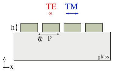
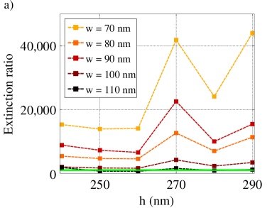
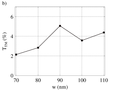
Previous studies [17] indicate typical grating parameters, and a period of nm seems to deliver good performances around nm. In this regime the condition is not fulfilled, therefore the Effective Medium Theory (EMT) cannot be used. The optimisation of the slit width as well as the gold thickness was thus studied using FDTD simulations (MEEP [18]). This simulation program uses the Lorentz-Drude dispersion model with optical constants obtained from thin films measurements [19]. Due to the very long computation time associated with a resonant structure, the spatial resolution was limited to 7 nm. Figure LABEL:sub@hw shows the dependence of the extinction ratio on the thickness and the slit width. Beyond nm, the ER reaches very high values but we rather concentrate on the first vertical resonance at nm, as the fabrication of very narrow slits with straight flanks becomes more difficult with increasing metal thickness. We also observe on Fig. LABEL:sub@terect a horizontal resonance at nm, where the ER increases due to higher transmission of the TM-modes.
3 Fabrication and characterisation
A 170 µm thick glass substrate was coated with 3 nm Titanium (adhesion layer) followed by 265 nm gold using Electron Beam Physical Vapour Deposition. Deposition rates were maintained relatively low (below 1.5) to minimise the granularity and the surface roughness of the layers. Although simulations indicate a resonance for nm, better performances were experimentally observed for nm. This shift was also predicted by additional high-resolution simulations taking into account the presence of the adhesion layer. The theoretical ER obtained for the experimental configuration is nevertheless comparable with the one resulting from the simple model of gold (nm) on a glass plate. The subwavelength gratings (120120 µm) were then engraved using the Focused Ion Beam (FIB) milling technique (Zeiss Cross-Beam) at the Center for Nanostructures and Nanomaterials (ZNN, Munich, Germany). The wire-grid polarisers were characterised by measuring the ER for well-defined input polarisations. While this study focuses on performance at 850 nm, we refer the reader to [12] for similar numerical and experimental results including wavelength dependence.
| Sample | (nm) | ER (experimental) | ER (simulated) |
|---|---|---|---|
| 120 | 380 | 2520 | |
| 120 | 650 | ||
| 80 | 720 | 12700 | |
| 80 | 850 |
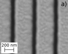
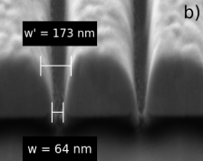
According to the simulations, an extinction ratio above 2,000 should be obtained for slit widths below 120 nm. The first sample was fabricated with this largest possible width (Samples , see Table 1), yet the measured values did not exceed 1:650. In order to achieve the desired performances, new samples with smaller slit widths were manufactured. Although the experimental ER slightly increases for nm, the simulations indicate a much stronger increase by at least a factor of 10. Moreover, the measured ER shows a large scatter for different samples although the gratings exhibit a similar geometry and roughness in top view SEM pictures, typically similar to Fig. LABEL:sub@st. A significant difference appears when investigating the cross-section of the gold stripes using FIB milling. The side-view SEM pictures in Fig. LABEL:sub@sc now reveal a rather trapezoidal profile, with a non negligible difference between the lower and upper base lengths of about 100 nm. This shape results from side redeposition of the ablated material during the milling of the stripes, which can be potentially reduced by using a multi-pass FIB writing mode.
4 Grating optimisation with realistic geometrical model
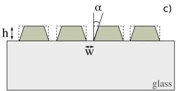
In order to understand the often reported reduced performances of the manufactured WGP compared to predictions, a deeper study involving further simulations has been carried out. To account for the observed geometry we introduce a refined model based on a more realistic trapezoidal stripe shape. The parameter now denotes the slit width at the bottom of the stripes, close to the substrate, and the angle corresponds to the deviation from a perfect rectangular structure, as illustrated in Fig. LABEL:sub@pol_geometry.
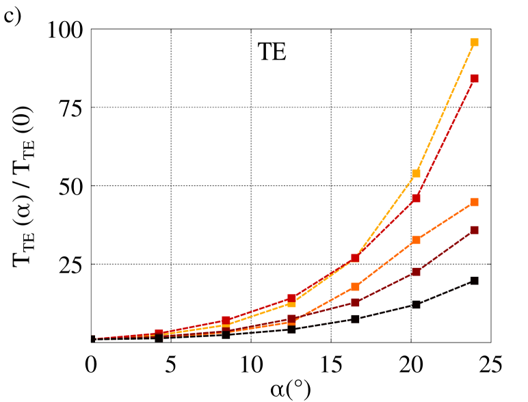
The transmission of both TE and TM modes, as well as the ER are computed varying again the slit width and additionally the opening angle . Figure LABEL:sub@er shows an exponential decrease of ER when varying the angle , but also that the trapezoidal shape leads to slightly higher transmissions for the TM modes, see Fig. LABEL:sub@tte. This is consistent with the case for rectangular shape, where increases with . This effect is nonetheless reduced in the case of the resonance (nm). While the influence of on TM-states is limited, it has dramatic consequences for the TE-polarisation, as can be seen in Fig. LABEL:sub@ttm. In this case we observe an exponential increase of the transmission with the opening angle, which consequently leads to the exponential decrease of the ER. When using the trapezoidal shape in the simulations, the theoretical ER values are reduced from 12700 (rectangular stripes, nm) down to 500 for () and 2700 for (). This trapezoidal shape indeed explains the order of magnitude discrepancy observed between simulations of perfectly rectangular stripes and realistic samples.



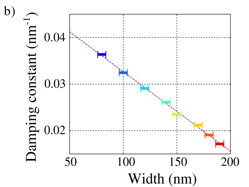
Since is largely independent of the angle , it is the dependence of the transmission of the TE-mode which determines the . A closer inspection adopting the model of guided waves in the slit [20] shows that the TE-mode is exponentially damped as the wavelength of the incoming field is above the cut-off wavelength. Figure LABEL:sub@fields shows exemplarily the result of the numerical simulations for two different heights. Evidently, the field is exponentially damped when propagating through the slit, which also explains the exponential dependence of the transmission on the metal thickness. Analysing the dependence of the damping coefficient on the slit width shows an approximately linear behaviour in the region of relevant slit widths in Fig. LABEL:sub@decay, which is also in good agreement with calculations of effective refraction indices in previous studies [21]. Given smooth variation of the slit width, and thus ER can be well approximated taking the effective, i.e., averaged, width of the slits into account. Figure LABEL:sub@weff shows that the unnormalised values of for different average slit widths are indeed approximately independent of the angle .

Using these findings for the next optimisation step, we note that the targeted extinction ratio of 1,000 can be achieved for rectangular stripes with nm, but not for achievable angles . Yet, reducing the slit width down to nm (corresponding to nm) brings a clear improvement. This simulation was verified experimentally by the fabrication of a new polariser array, presented in Fig. 6. Table 2 presents the characterisation of these four samples and compares them to the theoretical performances simulated with the refined model. As expected, the ER exceeds 1,000 and even reaches 1,800, yielding the best ER observed so far for 850 nm. The transmission is similar for all samples and reaches 9 %. The simple simulation model based on trapezoidal stripes is therefore suited for realistic devices as it exhibits excellent agreement with the experimental data.
The remaining difference between experiment and theory is most likely due to the spatial resolution of the simulation and the measurement uncertainty of on the SEM image, as well as the aforementionned effect of the adhesion layer. According to recent studies [22], surface roughness should not degrade the performance significantly. In addition, the trapezoidal shape smoothens the field distribution compared to rectangular shapes, further reducing the influence of surface irregularities.
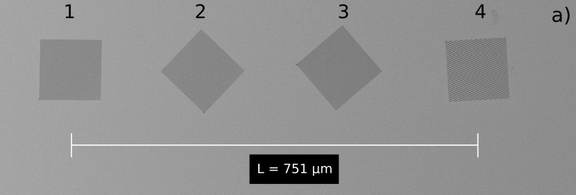
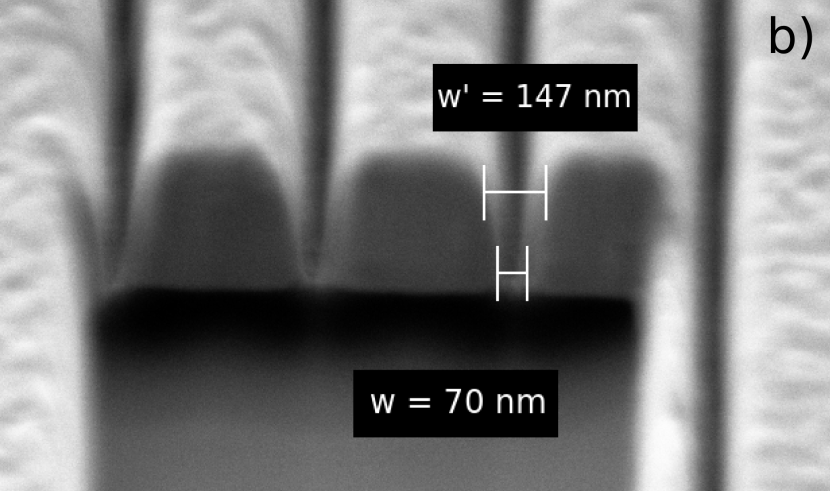
| Sample | (nm) | (nm) | (o) | ER (experimental) | ER (simulated) |
|---|---|---|---|---|---|
| 1 | 70 | 150 | 16 | 1800 | 4200 |
| 2 | 70 | 160 | 19 | 1620 | 2870 |
| 3 | 80 | 160 | 16 | 1200 | 1510 |
| 4 | 70 | 175 | 21 | 1150 | 1544 |
5 Conclusion
We presented clear evidence of the impact of geometrical deviations from perfect rectangular cross-section onto the performance of wire-grid-polarisers. Transversal SEM pictures indicate a trapezoidal shape of the stripes, a defect present with all currently used fabrication techniques. While better rectangular stripe profiles could be achieved, there will always be some imperfections left. Nevertheless, the real performance of wire-grid polarisers can be well simulated when accounting for the true shape of the wires or in a first approximation for the effective slit width. High extinction ratios can be achieved even with imperfect structures when optimising other parameters. Comparison between experiments and simulations shows, for the first time, significantly improved agreement, with experimental devices reaching extinction ratios of up to 1,800 and transmission of % at 850 nm.
Acknowledgements
The authors acknowledge technical help from P. Altpeter (LMU), P. Weiser and S. Matich (ZNN) regarding the fabrication of the polarisers . This project was funded by the excellence cluster Nano-Initiative Munich (NIM) and by the European projects CHIST-ERA/QUASAR, FP7/QWAD and FP7/CIPRIS.