Quasiparticle Band Gaps, Excitonic Effects, and Anisotropic Optical Properties of Monolayer Distorted 1-T Diamond-Chain Structure ReS2 and ReSe2
Abstract
We report many-body perturbation theory calculations of excited-state properties of distorted 1-T diamond-chain monolayer rhenium disulfide (ReS2) and diselenide (ReSe2). Electronic self-energy substantially enhances their quasiparticle band gaps and, surprisingly, converts monolayer ReSe2 to a direct-gap semiconductor, which was, however, regarded to be an indirect one by density-functional-theory calculations. Their optical absorption spectra are dictated by strongly bound excitons. Unlike hexagonal structures, the lowest-energy bright exciton of distorted 1-T ReS2 exhibits a perfect figure-8 shape polarization dependence but those of ReSe2 only exhibit a partial polarization dependence, which results from two nearly-degenerated bright excitons whose polarization preferences are not aligned. Our first-principles calculations are in excellent agreement with experiments and pave the way for optoelectronic applications.
pacs:
71.35.-y, 31.15.A-, 73.22.-f, 78.67.-nI Introduction
To overcome the zero band gap of graphene neto2009electronic , two-dimensional (2D) transition-metal dichalcogenides (TMDCs) semiconductors have attracted significant attention wang2012electronics ; mak2010atomically ; wang2010 ; yao2012 ; feng2012 . Thanks to the very thin atomic thickness (a few Å), pristine interfaces without out-of-plane dangling bonds, and considerable band gaps (1-2 eV) mos2-1 ; mos2-2 ; wang2012electronics ; qiu2013optical ; yang2013 , TMDCs are potentially beneficial for eliminating short channel effects liu2012channel , lowering interface state densities, reducing surface roughness scattering geim2013van , and low-power digital applications radisavljevic2011single ; chuang2014high ; liu2013role ; das2012high . However, because of interlayer interactions and variations of screening, the electronic structures of many hexagonal TMDCs undergo substantial variations with different stacking layer numbers. For example, a crossover from direct band gaps in monolayers to indirect band gaps in multilayers has been observed in MoS2 mak2010atomically ; wang2010 ; zhang2014direct , limiting the applicability of TMDCs in optoelectronic devices.
Layered crystals of rhenium disulfide (ReS2) and diselenide (ReSe2) are a new family of 2D TMDCs semiconductors, which have been successfully fabricated recently tongay2014monolayer ; yang2014layer ; wolverson2014raman . Unlike hexagonal TMDCs, ReX2 (X= S, Se) crystallizes in a distorted 1-T diamond-chain structure with the triclinic symmetry, as a result of charge decoupling from an extra valence electron of Re atoms tongay2014monolayer ; yang2014layer ; wolverson2014raman . This structural distortion leads to a much weaker interlayer coupling. Consequently, the band renormalization is absent and bulk ReX2 behaves as electronically and vibrationally decoupled monolayers tongay2014monolayer ; yang2014layer . Such a vanishing interlayer coupling in ReX2 structures enables probing 2D-like systems without the need of monolayer or few layers, overcoming the challenge of preparing large-area, single-crystal monolayers tongay2014monolayer . Furthermore, the structure distortion of 1T-ReX2 makes it exhibit unique anisotropic optical, electrical, and mechanical properties tongay2014monolayer ; wolverson2014raman , with considerable interests for various applications in polarization controller, liquid crystal displays, 3D visualization techniques, (bio)dermatology, and in optical quantum computers nan2009linear ; knill2001scheme .
Despite these unique properties and potential applications of distorted 1-T diamond-chain ReX2 structures, we have very limited knowledge about their fundamental excited-state properties, such as quasiparticle band gaps, optical spectra, and excitonic effects. In particular, currently available experimental measurements are diverse due to sample qualities and unavoidable environment effects. In this sense, a reliable and parameter-free calculation to accurately capture essential electron-electron (e-e) and electron-hole (e-h) interactions in excited-state properties is highly desirable for understanding fundamental physics and motivating applications of few-layer ReX2.
In this work, we employ the first-principles GW-Bethe-Salpeter Equation (BSE) approach to study two typical distorted 1-T diamond-chain TMDCs, i.e., monolayer ReS2 and ReSe2. We observe significant many-electron effects that dictate their excited-state properties. Self-energy corrections not only enlarge band gaps but also convert suspended monolayer ReSe2 to be a direct-gap semiconductor. Excitonic effects are prominent and the BSE-calculated absorption spectra are in excellent agreement with measurements. In particular, because of the reduced triclinic symmetry, monolayer ReS2 and ReSe2 possess anisotropic optical responses within the near-infrared frequency regime. These excited-state properties within the interesting frequency regime may be useful for optoelectronic applications.
The remainder of this paper is organized as follows: In Sec. II, we introduce the atomic structures of monolayer ReS2 and ReSe2, and our computational approaches. In Sec. III, the quasiparticle band energies, band gaps, and the transition from indirect to a direct band gap, are presented. In Sec. IV, we discuss the optical absorption spectra and excitonic effects. In Sec. V, we focus on the anisotropic optical responses of excitons. In Sec. VI, we summarize our studies and conclusion.
II Atomic Structure and Computational Methods
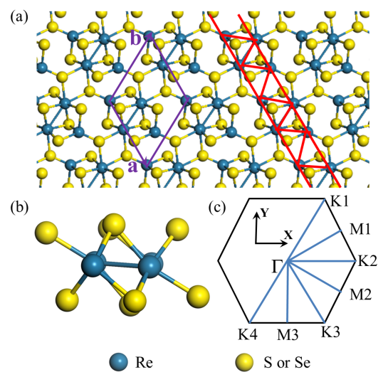
The ball-stick structures of monolayer distorted 1-T diamond-chain ReS2 and ReSe2 are presented in Fig. 1. The unit cell and unit vectors are marked by purple-colored vectors. Each Re atom is clustering of “diamond chains” composed of the zigzag shape along the a direction as shown by red-colored lines in Fig. 1(a) tongay2014monolayer ; horzum2014formation ; corbet2014field ; yang2015tuning . The side view of monolayer ReS2 or ReSe2 is presented in Fig. 1(b). The special feature is that, unlike hexagonal TMDCs, the S or Se atoms of distorted 1-T diamond-chain structures are not all in the same plane, substantially lowering the structure symmetry. The first Brillouin zone (BZ) is plotted in Fig. 1(c), which is a hexagon but with unequal side lengths as a result of the distorted atomic structure. Consequently, the K1, K2, and K3 points are no longer equivalent.
We fully relax the structures according to the force and stress calculated by DFT with the Perdew, Burke, and Ernzerhof (PBE) functional perdew1996generalized , using the Quantum Espresso package giannozzi2009quantum . The ground-state wave functions and eigenvalues are obtained from the DFT/PBE with norm-conserving pseudopotentials troullier1991efficient . The plane-wave basis is set with a cutoff energy of 60 Ry with a -point grid. A vacuum space between neighboring layers is set to be more than 25 Å to avoid the interactions between layers. Based on these parameters, our calculated lattice constant a is 6.43 (6.78) Å and the lattice constant b is 6.53 (6.66) Å for ReS2 and ReSe2, respectively. They are consistent with previous calculations tongay2014monolayer ; wolverson2014raman .
The quasiparticle energies and band gaps are calculated by the GW approximation within the general plasmon pole (GPP) model hybertsen1986electron . The involved unoccupied conduction band number for calculating the dielectric function and self-energy is about ten times of the occupied valence band number. In solving the BSE, we use a finer -point grid of for converged excitonic states rohlfing2000electron . All the GW-BSE calculations are performed with the BerkeleyGW code berkeleyGW including the slab coulomb truncation scheme to mimic suspended monolayer structures ismail2006truncation ; rozzi2006exact . For optical absorption spectra, only the incident light polarized parallel with the plane is considered due to the depolarization effect spataru2004quasiparticle ; yang2007enhanced .
III Quasiparticle Energies and Band Gap
The DFT calculated band structures of monolayer ReS2 and ReSe2 are presented in Fig. 2. That with spin-orbit coupling (SOC) included is presented in the appendix. As shown in Fig. 2(a), monolayer ReS2 exhibits a 1.36 eV direct band gap at the point. This is consistent with a recent work tongay2014monolayer reporting a value of 1.43 eV. On the other hand, at the DFT level, monolayer ReSe2 is observed to be an indirect-gap semiconductor; the conduction band minimum (CBM) is located at the point while the valence band maximum (VBM) is slightly away from the point, as shown in Fig. 2(b) and its inset. The DFT-calculated indirect band gap of monolayer ReSe2 is about 1.22 eV and the direct gap at the point is slightly larger, about 1.25 eV. These are also consistent with previous DFT calculations yang2014layer ; wolverson2014raman ; yang2015tuning .
However, it is well known that DFT usually underestimates the band gap of semiconductors. Therefore, we have performed the GW calculation to obtain reliable quasiparticle band gaps of monolayer ReS2 and ReSe2. Similar to those found in other monolayer 2D semiconductors, such as monolayer hexagonal TMDCs (MoS2) mos2-1 ; mos2-2 ; qiu2013optical ; yang2013 and phosphorene tran2014layer , significant self-energy enhancements are observed in ReX2; at the ”single-shot” G0W0 level, the quasiparticle band gap of monolayer ReS2 is increased to be 2.38 eV and that of monolayer ReSe2 is increased to 2.09 eV, as listed in Table I. These enhanced many-electron effects are from the depressed screening and reduced dimensionality of suspended 2D semiconductors qiu2013optical ; tran2014layer ; mos2-1 ; shi2013quasiparticle .
Interestingly, the self-energy not only enlarges the band gap value but also may modify the band topology of ReX2. This is particularly significant for monolayer ReSe2, which is an indirect-gap semiconductor at the DFT level, as shown in Fig. 2(b). However, e-e interactions lower the valence band energy at the point by about 50 meV more, compared to that of the point. Therefore, the VBM is shifted to the point, making monolayer ReSe2 a direct-gap semiconductor, as listed in the blue-colored VBM in table II. However, it has to be pointed out that the indirect to direct transition may not be very sharp because the energy difference at the / point are very small and external perturbations may change the conclusion. On the other hand, it shall be true that the many-electron self-energy will increase the valence band energy at the point and, at least, make the top of valence band almost degenerated. This will affect photoluminescence (PL) experiments.
These different self-energy corrections are resulted from the nature of the involved electronic states at the and points. For example, a major contribution to the self-energy is from the screened-exchange interaction () hybertsen1986electron , which is strongly affected by the spatial localization of electronic states. This can be seen from its static form hybertsen1986electron :
| (1) |
where the subscripts is the band index and is the sampling points in the reciprocal space, is the electronic wave function, and is the screened Coulomb interaction. Obviously, a smaller distance between and enhances the overlap between wave functions and screened Coulomb interactions, giving rise to a larger self-energy. This non-uniform self-energy correction is similar to what have been observed in hexagonal TMDCs, i.e., the different self-energy corrections at the K point and the zone center of monolayer MoS2 qiu2013optical . Following this idea, we have checked the projected density of states (PDOS) of electronic states at the and points of ReSe2, as listed in Table 2. The valence state has more localized -electron component (86%) than that the valence state (78%). As a result, quasiparticle energy of the state is enhanced more, meaning its energy level is lowered more and resulting in a switch of the VBM.
This direct quasiparticle band gap is not conflicted with experimental measurements, in which rather weak PL peak intensity is observed in monolayer ReSe2 and the PL peak of ReSe2 increases monotonically with increasing the layer number zhao2015interlayer . This measurement seems to hint an indirect-gap of ReSe2. However, different from our calculated suspended and neutral cases, these measured samples are on substrates and are inevitably doped. Thus their self-energy corrections will be substantially reduced under these conditions, as shown in WSe2 and MoS2 louie2014 ; yang2015 , meaning their measured samples may have a slightly indirect band gap. It has to be pointed out that this small energy difference is within the intrinsic error bars of DFT and GW methods. Thus more accurate experiments of suspended samples are important for conclusive results.
Finally, previous works have shown that the self-consistent GW (sc-GW) scheme beyond single-shot calculations may be necessary for 2D semiconductors shi2013quasiparticle ; qiu2013optical ; tran2014layer . Therefore, we perform one self-consistent update to the Green’s function G; the quasiparticle band gap is further increased to 2.82 eV for monolayer ReS2 and 2.45 eV for monolayer ReSe2, as listed in Table 1. Similar to monolayer MoS2 and black phosphorus, we find that more self-consistent steps only slightly change the band gap () and we stop at the sc-G1W0 level. Finally, the SOC is significant in ReX2 structures (around 150 meV of lowering the band gap) tongay2014monolayer . Considering all these factors, we compute the quasiparticle band gaps and summarize them in the last column of Table 1. In the following, all our discussions and the BSE calculations are based on the finalized sc-G1W0 results with SOC included.
IV Exciton Effects on Optical Absorption Spectra
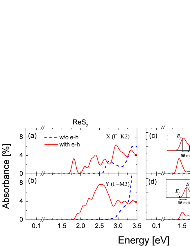
Because optical spectra of ReX2 are anisotropic, we first focus on those with the incident light polarized along the -K2 (x) directions because the corresponding optical absorption spectra can exhibit most features. Those of other polarizations will be discussed in Section V. First, the single-particle optical absorption spectra for monolayer ReS2 and ReSe2 are presented in Figs. 3(a) and (c) (blue dashed lines). As expected, the main optical absorption shoulder starts from the quasiparticle band gap, which are around 2.7 eV and 2.3 eV, for ReS2 and ReSe2, respectively.
Since e-h interactions are known to be crucial for obtaining reliable optical spectra in 2D semiconductors, we have solved the BSE to include them and present the optical absorption spectra in Fig. 3 by red solid lines. Similar to other 2D semiconductors, all main optical features are dominated by excitonic states in monolayer ReX2. For example, after including e-h interactions, the first absorption peak of ReS2 is located at 1.63 eV as shown in Fig. 3(a), which is a strongly bound exciton with a 1.07-eV e-h binding energy. Monolayer ReSe2 exhibits similarly enhanced excitonic effects as shown in Fig. 3(c) with the absorption peak at around 1.42 eV and exciton binding energy of 0.87 eV.
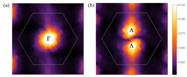
It has to be pointed out that the lowest-energy peak (1.42 eV) in the optical absorption spectrum of monolayer ReSe2 is actually composed of two bright excitons ( and ), as elucidated in the insert of Fig. 3(c). The energy spacing of these two excitons is only about 96 meV. These two nearly degenerated excitons are resulted from the indirect-gap nature of ReSe2. To see this, we have plotted the distributions of these exciton amplitudes in the reciprocal space (see details in Ref. qiu2013optical, ). As shown in Fig. 4, the exciton is mainly from the transitions around the zone center (the point), while the exciton is mainly from those around the points. Since the energies of maxima of the valence band at the and points are very close to each other, the formed excitons obviously have very similar energies as well.
Recently, several PL measurements of monolayer ReS2 and ReSe2 have been performed. The measured broad PL peak position is about 1.50 to 1.65 eV at room temperature for ReS2 tongay2014monolayer ; horzum2014formation and 1.47 eV for ReSe2 yang2015tuning . These experimental observations are in excellent agreement with our first-principles calculations, which we calculate as 1.6 eV and 1.4 eV for ReS2 and ReSe2, respectively. As shown in many previous works rubio2006 ; komsa2012 ; louie2014 , the quasiparticle self-energy and e-h interactions partially cancel each other, making the final “optical” gap not much larger than the DFT-calculated band gap.
Finally, we have to address that Coulomb truncation is crucial for all above calculations komsa2012 ; wirtz2013 . Without Coulomb truncation, both self-energy corrections and excitonic effects will be reduced because the actual simulation object is periodic structures with a large interlayer distance. For instance, for monolayer black phosphorus tran2014layer , the GW calculation with Coulomb truncation gives the band gap as 2 eV while that without truncation gives the value of 1.7 eV.
V Anisotropic Exciton
Unlike hexagonal TMDCs, monolayer ReS2 and ReSe2 are the distorted 1-T diamond-chain with the triclinic symmetry. As a result, the optical absorption may be also anisotropic. This has been previously examined at the DFT level ho2004optical , where it is determined that the absorption spectra are anisotropic with respect to the polarization direction of the incident light. However, due to the incorrect band gaps and the short of e-h interactions, those DFT-calculations cannot be directly compared with experiments for providing reliable understanding. This motivates us to study the anisotropic optical responses at the level of including quasiparticle energy and excitonic effects.
Let us first focus on the case of monolayer ReS2. Its symmetry-induced anisotropic optical response can be seen even at the single-particle optical absorption level. As shown in Figs. 3(a) and (b), the single-particle optical absorption spectrum begins at near 2.7 eV for the incident light polarized along the -K2 (x) direction, while it becomes significant at 2.9 eV for the light polarized along the -M3 (y) direction. Previous studies have discussed this optical anisotropy ho2004optical ; ho2001plane and it is attributed to the transitions from non-bonding Re 5 to 5 and to anti-bonding chalcogen and states ho2004optical . In Table 2, we have listed the PDOS of band-edge states of monolayer Res2 and ReSe2. It is clear that both valence and conduction band edges are mainly made of Re 5 states and chalcogen states. For example, the state of ReS2 has 11 percents of state of S atoms and 80 percents of state of Re atoms. This is consistent with previous studies ccakir2014doping .
The inclusion of e-h interactions does not essentially change the anisotropic optical response. As shown by red solid lines in Figs. 3(a) and (b), excitonic effects only lower the absorption edge but keep the anisotropy. For example, the lowest-energy excitonic peak of monolayer ReS2 is at 1.63 eV for the incident light polarized along the -K2 (x) direction and the absorption edge is located at 1.9 eV for the incident light polarized along the -M3 (y) direction. Thus monolayer ReS2 may work as an optical polarizer covering the frequency range from 1.6 eV to 1.9 eV, which is very interesting for near-infrared applications.
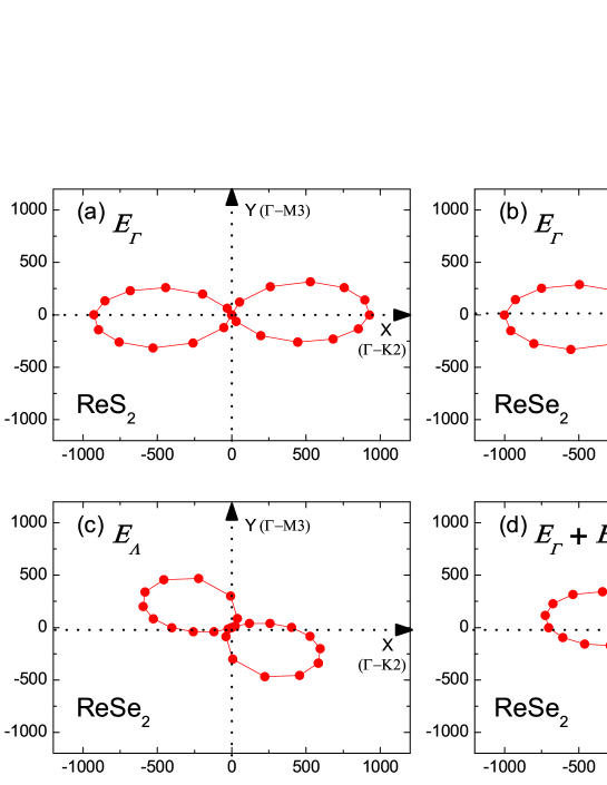
In order to have a complete picture of anisotropies of these important bright excitons, we present their optical oscillator strength with respect to the polarization angle of the incident light in Fig. 5. As expected, the optical oscillator strength of the prominent exciton of monolayer ReS2 exhibits a figure-8 shape (Fig. 5(a)), which represents the spatial anisotropic optical response. For different directions, the optical oscillator strength can differ by two orders of magnitude. For instance, the intensity along -K2 (x) direction is about 800 times stronger than that along -M3 (y) direction. This anisotropic response can easily be observed by both optical absorption and PL experiments.
Monolayer ReSe2 exhibits a similar anisotropic optical response, with some subtle differences. As shown in Figs. 3(c) and (d), the optical absorption spectra of monolayer ReSe2 are different with respect to the polarization direction of incident light. However, the lowest-energy absorption peak (around 1.4 eV) along the -K2 (x) direction does not completely disappear for the incident light polarized along the -M3 (y) direction. This is different from the case of ReS2. This complication arises from the fact that the lowest-energy peak of ReSe2 actually consists of two excitons ( and ), instead of one in ReS2, as shown in the insert of Figs. 3(c) and (d). behaves similar to the lowest exciton in ReS2, which is bright when the incident light is polarized along the -K2 (x) direction, and dark along the -M3 (y) direction. , on the other hand, is not completely dark along the -M3 (y) direction. Thus the lowest-energy peak does not have an extremely high polariztion anisotropy.
This can be better understood by plotting the oscillator strength of the excitons and seperately, which is shown in Figs. 5(b) and (c). Interestingly, both excitons, and , exhibit significant spatial anisotropy. However, the preferred direction of the exciton is rotated by about 30 degrees. This is not surprising since the main contribution of the exciton is from those states at the points, which are not high-symmetry points. Finally, because the prominent absorption peak at 1.4 eV is the combination of these two excitons, it is obvious that the overall optical absorption does not show a complete anisotropy as shown in Fig. 5(d) with a 50-meV smearing. It has to be pointed out that PL experiments may exhibit stronger anisotropic optical spectra than the absorption measurements. At room temperature, the 96-meV gap between the excitons and will make most excited carriers collected by the lower-energy exciton, resulting in a simpler anisotropic PL intensity similar to the exciton shown in Fig. 5(b).
VI Summary
In summary, first-principles GW-BSE simulations have been performed to study quasiparticle band gaps, excitonic effects, and optical spectra of distorted 1-T diamond-chain monolayer ReS2 and ReSe2. Monolayer ReS2 is direct band gap semiconductor, and the quasiparticle band gap is 2.7 eV. Monolayer ReSe2 changes from the DFT-calculated 1.22-eV indirect band gap to be a 2.3-eV direct one after GW corrections. Huge excitonic effects dominate optical spectra of suspended monolayer ReX2, with around 1-eV e-h binding energies. The calculated absorption peaks are in excellent agreement with recent measurements. Additionally, both the monolayer ReS2 and ReSe2 shows anisotropic optical responses due to their reduced triclinic symmetry lattices. In particular, the partially anisotropic optical absorption spectra of monolayer ReSe2 are attributed to the two adjacent excitons, resulting from two nearby maxima at the valence band edge. Our calculations provide necessary information to clarify experimental measurements and our predictions are useful for broad near-infrared applications of distorted 1-T phase 2D semiconductors.
Acknowledgements.
We thank Vy Tran, Ruixiang Fei, and Han Wang for fruitful discussions. This work is supported by National Science Foundation Grant No. DMR-1207141. H.-X. Z. and J.-J. S. are supported by the National Basic Research Program of China (No. 2012CB619304) and the National Natural Science Foundation of China (No. 11474012). H.-X. Z. also acknowledges the financial support from the China Scholarship Council. The computational resources have been provided by the Lonestar of Teragrid at the Texas Advanced Computing Center (TACC).References
- (1) A. H. Castro Neto, F. Guinea, N. M. R. Peres, K. S. Novoselov, and A. K. Geim, Rev. Mod. Phys. 81, 109 (2009).
- (2) Q. H. Wang, K. Kalantar-Zadeh, A. Kis, J. N. Coleman, and M. S. Strano, Nat. Nanotechnol. 7, 699-712 (2012).
- (3) A. Splendiani, L. Sun, Y. Zhang, T. Li, J. Kim, C.-Y. Chim, G. Galli, and F. Wang, Nano. Lett. 10, 1271-1275 (2010).
- (4) K. F. Mak, C. Lee, J. Hone, J. Shan, and T. F. Heinz, Phys. Rev. Lett. 105, 136805 (2010).
- (5) D. Xiao, G.-B. Liu, W. Feng, X. Xu, and W. Yao, Phys. Rev. Lett. 108, 196802 (2012).
- (6) T. Cao, G. Wang, W. Han, H. Ye, C. Zhu, J. Shi, Q. Niu, P. Tan, E. Wang, B. Liu, and J. Feng, Nat. Comm. 3, 887 (2012).
- (7) A. Ramasubramaniam, Phys. Rev. B 86, 115409 (2012).
- (8) H. Shi, H. Pan, Y.-W. Zhang, and B. I. Yakobson, Phys. Rev. B 87, 155304 (2013).
- (9) D. Y. Qiu, F. H. da Jornada, and S. G. Louie, Phys. Rev. Lett. 111, 216805 (2013).
- (10) Y. Liang, S. Huang, R. Soklaski, and L. Yang, Appl. Rev. Lett. 103, 042106 (2013).
- (11) H. Liu, A. T. Neal, and P. D. Ye, ACS Nano 6, 8563-8569 (2012).
- (12) A. Geim and I. Grigorieva, Nature 499, 419-425 (2013).
- (13) B. Radisavljevic, A. Radenovic, J. Brivio, V. Giacometti, and A. Kis, Nat. Nanotechnol. 6, 147-150 (2011).
- (14) H.-J. Chuang, X. Tan, N. J. Ghimire, M. M. Perera, B. Chamlagain, M. M.-C. Cheng, J. Yan, D. Mandrus, D. Tom nek, and Z. Zhou, Nano lett. 14, 3594-3601 (2014).
- (15) W. Liu, J. Kang, D. Sarkar, Y. Khatami, D. Jena, and K. Banerjee, Nano lett. 13, 1983-1990 (2013).
- (16) S. Das, H.-Y. Chen, A. V. Penumatcha, and J. Appenzeller, Nano lett. 13, 100-105 (2013).
- (17) Y. Zhang, T.-R. Chang, B. Zhou, Y.-T. Cui, H. Yan, Z. Liu, F. Schmitt, J. Lee, R. Moore, Y. Chen, et al., Nat. Nanotechnol. 9, 111-115 (2014).
- (18) S. Tongay, H. Sahin, C. Ko, A. Luce, W. Fan, K. Liu, J. Zhou, Y.-S. Huang, C.-H. Ho, J. Yan, et al., Nat. Commun. 5, 3252 (2014).
- (19) S. Yang, S. Tongay, Y. Li, Q. Yue, J.-B. Xia, S.-S. Li, J. Li, and S.-H. Wei, Nanoscale 6, 7226-7231 (2014).
- (20) D. Wolverson, S. Crampin, A. S. Kazemi, A. Ilie, and S. J. Bending, ACS Nano 8, 11154-11164 (2014).
- (21) Z. Nan, J. Xiaoyu, G. Qiang, H. Yonghong, and M. Hui, Appl. Opt. 48, 6734-6739 (2009).
- (22) E. Knill, R. Laflamme, and G. J. Milburn, Nature (London) 409, 46-52 (2001).
- (23) S. Horzum, D. Cakir, J. Suh, S. Tongay, Y.-S. Huang, C.-H. Ho, J. Wu, H. Sahin, and F. Peeters, Phys. Rev. B 89, 155433 (2014).
- (24) C. M. Corbet, C. McClellan, A. Rai, S. S. Sonde, E. Tutuc, and S. K. Banerjee, ACS Nano 9, 363 (2014).
- (25) S. Yang, C. Wang, H. Sahin, H. Chen, Y. Li, S.-S. Li, A. Suslu, F. M. Peeters, Q. Liu, J. Li, et al., Nano lett. 15, 1660-1666 (2015).
- (26) L. Wirtz, A. Marini, and A. Rubio, Phys. Rev. Lett. 96, 126104 (2006).
- (27) H.-P. Komsa and A.V. Krasheninnikov, Phys. Rev. B 86, 241201(R) (2012).
- (28) M.M. Ugeda, A.J. Bradley, S.-F. Shi, F.H. da Jornada, Y. Zhang, D.Y. Qiu, W. Ruan, S.-K. Mo, Z. Hussain, Z.-X. Shen, F. Wang, S.G. Louie, and M.F. Crommie, Nature Mater. 13, 1091 (2014).
- (29) A. Molina-S nchez, D. Sangalli, K. Hummer, A. Marini, and L. Wirtz, Phys. Rev. B 88, 045412 (2013).
- (30) J. P. Perdew, K. Burke, and M. Ernzerhof, Phys. Rev. Lett. 77, 3865 (1996).
- (31) P. Giannozzi, S. Baroni, N. Bonini, M. Calandra, R. Car, C. Cavazzoni, D. Ceresoli, G. L. Chiarotti, M. Cococcioni, I. Dabo, et al., J. Phys.: Condens. Matter 21, 395502 (2009).
- (32) N. Troullier and J. L. Martins, Phys. Rev. B 43, 1993 (1991).
- (33) M. S. Hybertsen and S. G. Louie, Phys. Rev. B 34, 5390 (1986).
- (34) M. Rohlfing and S. G. Louie, Phys. Rev. B 62, 4927 (2000).
- (35) J. Deslippe, G. Samsonidze, D. A. Strubbe, M. Jain, M. L. Cohen, and S. G. Louie, Comput. Phys. Commun. 183, 1269 (2012).
- (36) S. Ismail-Beigi, Phys. Rev. B 73, 233103 (2006).
- (37) C. A. Rozzi, D. Varsano, A. Marini, E. K. Gross, and A. Rubio, Phys. Rev. B 73, 205119 (2006).
- (38) C. D. Spataru, S. Ismail-Beigi, L. X. Benedict, and S. G. Louie, Appl. Phys. A: Mater. Sci. Process. 78, 1129-1136 (2004).
- (39) L. Yang, C. D. Spataru, S. G. Louie, and M.-Y. Chou, Phys. Rev. B 75, 201304 (2007).
- (40) V. Tran, R. Soklaski, Y. Liang, and L. Yang, Phys. Rev. B 89, 235319 (2014).
- (41) C. D. Spataru, S. Ismail-Beigi, L. X. Benedict, and S. G. Louie, Phys. Rev. Lett. 92, 077402 (2004).
- (42) H. Shi, H. Pan, Y.-W. Zhang, and B. I. Yakobson, Phys. Rev. B 87, 155304 (2013).
- (43) H. Zhao, J. Wu, H. Zhong, Q. Guo, X. Wang, F. Xia, L. Yang, P.-H. Tan, and H. Wang, arXiv:1504.07664 (2015).
- (44) Y. Liang and L. Yang, Phys. Rev. Lett. 114, 063001 (2015).
- (45) C. Ho and C. Huang, J. Alloys Compd. 383, 74-79 (2004).
- (46) C. Ho, Y. Huang, and K. Tiong, J. Alloys Compd. 317, 222-226 (2001).
- (47) D. akir, H. Sahin, and F. M. Peeters, Phys. Chem. Chem. Phys. 16, 16771 (2014).
| DFT | G0W0 | sc-G1W0 | sc-G1W0(SOC) | |
|---|---|---|---|---|
| ReS2 | 1.36 | 2.38 | 2.82 | 2.69 |
| 1.43a | ||||
| ReSe2 | 1.22 | 2.09 | 2.45 | 2.29 |
| 1.24b |
| Energy (eV) | Re | X | ||||||
|---|---|---|---|---|---|---|---|---|
| DFT | G0W0 | |||||||
| ReS2 | 0.00 | 0.00 | 0 | 5 | 80 | 3 | 11 | |
| 1.36 | 2.38 | 1 | 2 | 69 | 1 | 27 | ||
| ReSe2 | -0.02 | 0.02 | 0 | 6 | 78 | 0 | 16 | |
| 1.22 | 2.11 | 0 | 1 | 59 | 1 | 39 | ||
| 0.00 | 0.00 | 0 | 4 | 86 | 0 | 10 | ||
| 1.29 | 2.18 | 0 | 1 | 63 | 1 | 35 | ||

*
Appendix A Band structure of monolayer ReX2 with SOC included
Since Re atoms are heavy atomic species, we thus take into accounts of SOC in Fig. 6. Compared with the band structures in Fig. 2. the SOC slightly reduces the band gap of monolayer ReX2, which is also clearly presented in Table I.
