Band gap and broken chirality in single-layer and bilayer graphene
Abstract
Chirality is one of the key features governing the electronic properties of single- and bilayer graphene: the basics of this concept and its consequences on transport are presented in this review. By breaking the inversion symmetry, a band gap can be opened in the band structures of both systems at the -point. This leads to interesting consequences for the pseudospin and, therefore, for the chirality. These consequences can be accessed by investigating the evolution of the Berry phase in such systems. Experimental observations of Fabry-Pérot interference in a dual-gated bilayer graphene device are finally presented and are used to illustrate the role played by the band gap on the evolution of the pseudospin. The presented results can be attributed to the breaking of the chirality in the energy range close to the gap.
I Introduction
Experimentally isolated in 2004 Novoselov et al. (2004), single-layer graphene (SLG) consists of a layer of carbon atoms, arranged in a honeycomb pattern. Its unit cell is defined by two carbon atoms, usually referred to as and , forming the two-atom basis of a Bravais lattice.
As predicted in Wallace (1947), it was experimentally demonstrated in that charge carriers in graphene behave like massless Dirac Fermions Novoselov et al. (2005); Zhang et al. (2005). They can be described by a two-component wavefunction obeying:
| (1) |
where is the Fermi velocity and is a vector of two Pauli matrices. Here, the analogy with quantum electrodynamics can be made by realizing that the two sublattices and play the role of spin-up and spin-down and that is not the spin but the pseudospin operator. The direction of motion is coupled to the pseudospin orientation, as one can see from Eq. (1), a property denoted as chirality. The chirality of charge carriers has important consequences for transport. It is responsible for a Berry phase of Novoselov et al. (2005); Zhang et al. (2005) and the suppression of backward scattering Katsnelson et al. (2006); Young and Kim (2009). These two effects are the basis of the Klein paradox Katsnelson et al. (2006); Klein (1929).
Bilayer graphene (BLG) also exhibits chiral charge carriers. However, instead of following the Klein physics, BLG exhibits anti-Klein properties, due to a Berry phase of Katsnelson et al. (2006); Novoselov et al. (2006). The concept of chirality in both single- and bilayer graphene and its presence in interference experiments is the focus of this review.
In Section II, we introduce the concept of chirality in SLG and BLG, and lay an emphasis on illustrating this concept, together with the concept of Berry’s phase. We then focus on several interference experiments, where signatures of the chirality were successfully observed. In Section III, we consider SLG and BLG systems in which the inversion symmetry has been lifted and a band gap has been opened in the band structure. We show that this lifting results in strong out-of-plane perturbations of the pseudospin in -space in the energy range close to the gap, but that the pseudospin orientation is further restored to its original state at higher energies. Finally, we focus on dual-gated BLG in Section IV and present an experiment allowing for the observation of the consequences of the opening of a band gap on the chirality, probed in a Fabry-Pérot interferometer geometry.
II Pseudospin and chirality
Charge carriers in graphene are chiral. This means that there is a handedness of their states because their pseudospin is locked to the direction of motion, giving rise to interesting tunneling properties that we review in this section.
II.1 Pseudospin motion in SLG and BLG
In graphene, low-energy charge carriers live around two inequivalent points in momentum space, and , called “valleys”. In the vicinity of the -point, single- and bilayer graphene can be described by the Hamiltonians Slonczewski and Weiss (1958); DiVincenzo and Mele (1984)
| (2) |
respectively, where is the momentum operator and is the effective mass. The above effective Hamiltonians are related to the tight-binding models through with and the intralayer nearest neighbor hopping energy and distance, respectively, and with the interlayer nearest neighbor hopping energy.
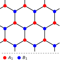
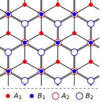
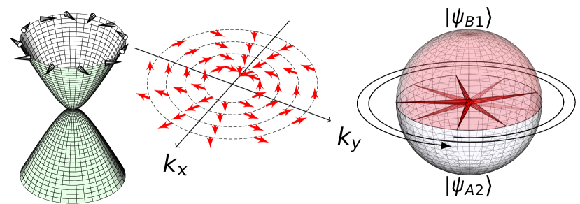
The Hamiltonians (2) act on the spinors and , respectively, where and are the two inequivalent carbon sites of a single-layer graphene and the indices and refer to the top and bottom layers of bilayer graphene; see Figs. 1a and 1b. This gives rise to the band structure shown in Fig. 2, left panels. Note however that the Hamiltonian (2) is a simplified two-band version, well-suited to describe the system at low energy. The full description would give rise to bands: two lower bands touching at the -point (seen in the figure) and two split bands, split away from the lower ones by the energy eV, not represented in the figure. In the following, we consider that we are in the low energy range, where only the lower bands are filled, as shown in Fig. 2.
The associated eigenstates are:
| (3) |
where the signs are related to the two eigenenergies and characterizes the direction of the wave vector measured from the -point. To better visualize the details of the motion of the pseudospin which is closely related to the Berry phase, we next introduce the polarization vector P as a convenient quantity.
In quantum mechanics, the polarization vector of a spin-1/2 quantum state is given by the expectation values of the Pauli matrices
| (4) |
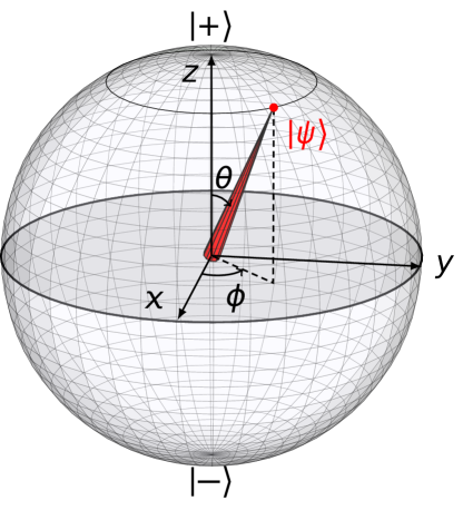
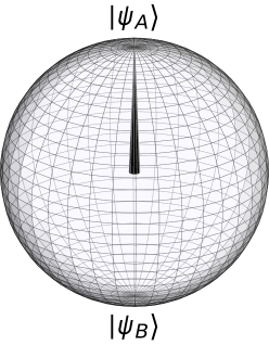
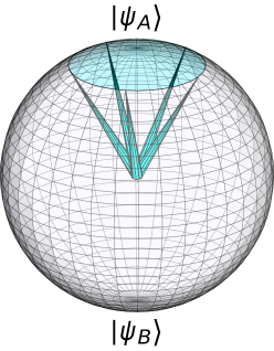
where is the polar angle and is the azimuthal angle Ihn (2010). This vector of length describes the spin orientation of and can conveniently be represented on the Bloch sphere Bloch (1946). Represented on such a Bloch sphere, the quantum state , which is a superposition of the two basis states and , together with its polarization vector are sketched in Fig. 1(c).
In the case of SLG and BLG, the polarization vector can be calculated by replacing in Eq. (4) with the eigenstates from Eq. (3), leading to
| (5) |
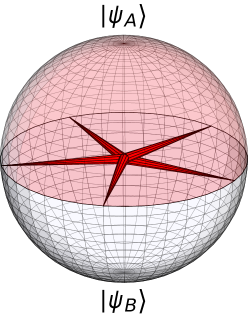
which describe, instead of the real spin, the pseudospin direction of and , respectively, and are particularly convenient for visualizing the motion of the pseudospin when the momentum rotates. The polarization vectors of Eq. (5) have no -component, due to the absence of diagonal terms in the Hamiltonians in Eq. (2). Thus both and depict a pseudospin restricted to the equatorial plane of the Bloch sphere (), as sketched in Fig. 2.
As indicated in Eq. (5), the pseudospin for the case of SLG rotates as fast as its wave vector [see Fig. 2(a)], while for BLG it winds twice as fast [see Fig. 2(b)]. In both cases, the process is only momentum-dependent but energy-independent. This is highlighted by the different constant energy cuts in each dispersion [middle panels of Figs. 2(a) and 2(b)], for the case of the conduction band. For the valence band, on the other hand, the pseudospin is inverted with respect to the point. This is referred to as a chirality for electrons (the pseudospin is always parallel to the wave vector) and for holes (the pseudospin is always anti-parallel to the wave vector) Haldane (1988). Since the two valleys exhibit opposite handedness, the reverse situation happens around the point, with chirality for the electrons and for the holes.
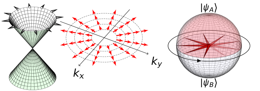
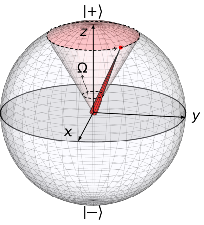
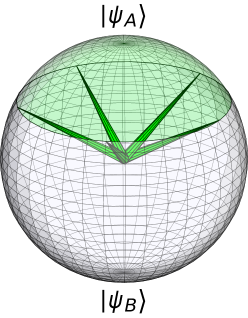
An important quantity closely related to the pseudospin motion is the Berry phase Berry (1984). The Berry phase, also known as a “geometrical phase” or “Pancharatnam phase”, is a phase acquired by a system during an adiabatic cyclic evolution. Upon adiabatic evolution along a closed path, the polarization vector defines a portion of the Bloch sphere and subtends a solid angle . An exemplary motion is shown in Fig. 1(d), where the polarization vector evolves along a circle of constant latitude at polar angle . In this case, the solid angle is given by . The Berry phase , i.e., the loop integral of the Berry connection, was found to be related to this quantity by Berry (1984); Anandan (1992); Xiao et al. (2010)
| (6) |
The Berry phase is half the solid angle subtended by the pseudospin during its motion. In case of an evolution in the equatorial plane (), as in the SLG case, the Berry phase (6) is equal to . In BLG, however, since the pseudospin rotates twice as fast as the momentum, the Berry phase is equal to [see right panels of Fig. 2(a)–(b)].
Hence, the Berry phase (in units of ) is equal to the number of rotations of the pseudospin when the wave vector completes one rotation around the point. This is why the Berry phase is often called the pseudospin winding number Park and Sim (2011). This integer number represents the degree of chirality McCann and Koshino (2013). Interestingly, this description is valid as well for multi-layer graphene. A -layer graphene system can be described by the Dirac-like Hamiltonian:
| (7) |
The corresponding Berry phase is accordingly McCann and Koshino (2013).
II.2 Transmission through a potential barrier
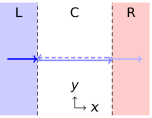
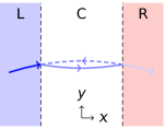
The pseudospin, as described above, leads to interesting properties when considering a charge carrier incident on a potential barrier. Consider the situation depicted in Fig. 3(a): a particle, moving from left (L region) to right (R region) in SLG, is incident at energy on a potential barrier (C region) of width . The barrier of height is further assumed to result in a junction (the prime referring to the C region), shifting the charge neutrality point as schematically displayed in Fig. 3(a). If the electron propagates ballistically in the regions away from the edges of the barrier potential, such a geometry resembles a Fabry-Pérot interferometer.
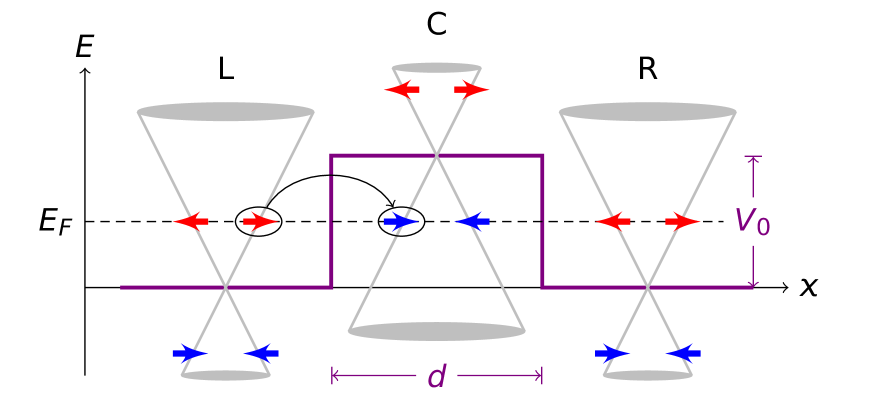
Focusing on the left interface of the barrier, we can see that a right moving electron (belonging to the right branch of the conduction band in the region L) will find a perfect match on the other side of the interface (C region), since a right moving hole exhibits the same pseudospin orientation, as highlighted in Fig. 3(a) with the encircled pseudospins. Such a situation implies a high transmission probability through the barrier. The exact solution to this problem has been investigated by Katsnelson et al. Katsnelson et al. (2006) in 2006 and described in detail in Ref. Tudorovskiy et al. (2012). For an electron wave of energy incident on a barrier of height , with translational invariance along the transverse direction , and holes populating the C region (), the resulting reflection coefficient was found to be:
| (8) | ||||
where and are the sign functions, and are the incident and refractive angles, and is the transmitted wave vector Katsnelson et al. (2006); Tudorovskiy et al. (2012). This enables the calculation of the transmission probability, given by . From this expression, one finds that normal incidence always leads to full transparency of the barrier (), known as the Klein tunneling in SLG.
Experimentally, such a graphene np’n junction can be realized by electrically controlling the carrier density inside and outside the barrier region. Considering densities outside the barrier region and within, we show two examples of with barrier thicknesses of in Fig. 4 (red curves), based on Eq. (8). These density values correspond to an incident energy of and a barrier height of . In these plots, we can see that the transmission probability at normal incidence is one, remains very high for small incident angles, and then exhibits additional full-transmission resonances at finite angles (sometimes) called ‘magic angles’.
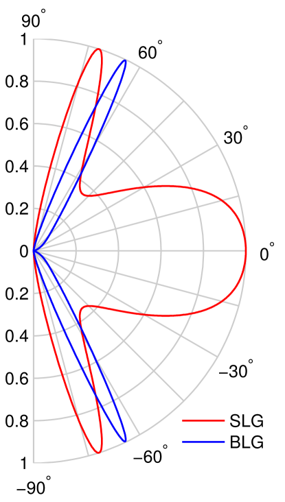
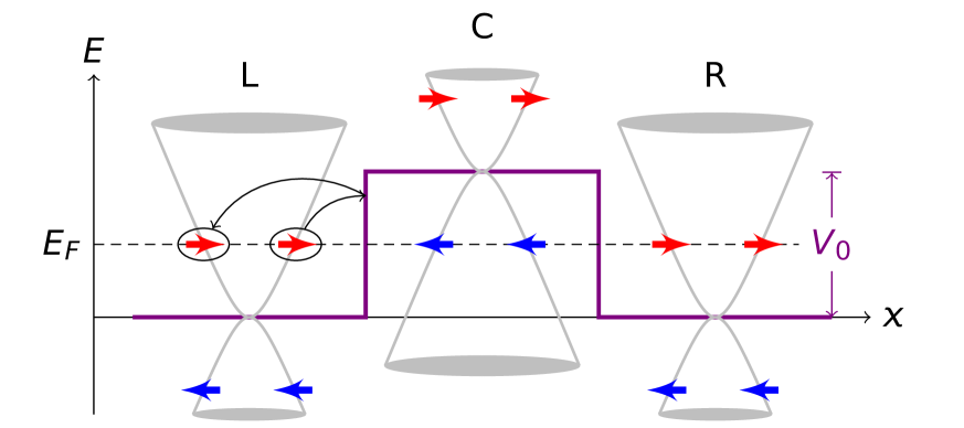
The same problem in the case of BLG was also treated in Katsnelson et al. (2006); Tudorovskiy et al. (2012) in the absence of the gap. The angle dependence of can be similarly obtained by solving the transmission problem. For a direct comparison to SLG, we consider the same and that lead to and show again two examples with barrier thicknesses in Fig. 4 (blue curves). Unlike for SLG, where massless Dirac fermions are always perfectly transmitted at normal incidence, a perfect reflection111This is true, however, only when where is the Fermi wavelength. In the case of , evanescent modes can lead to finite transmission even at normal incidence. at normal incidence is observed. This phenomenon is known as anti-Klein tunneling, and can be understood in terms of lack of pseudospin matching as sketched in Fig. 3(b).
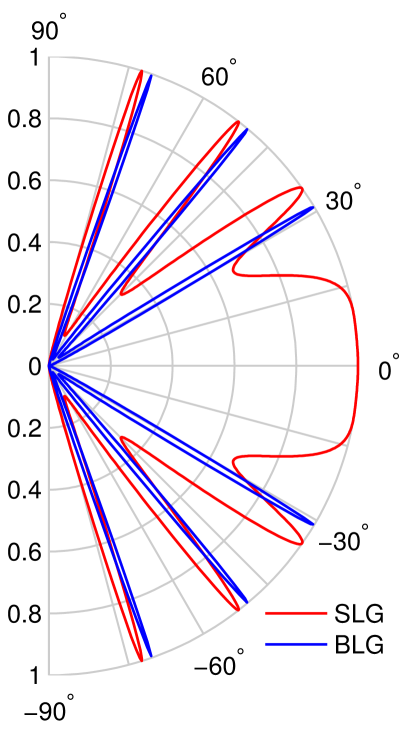
For non-zero incidence angles, some ‘magic angles’ appear, where the transmission increases sharply to one. The resulting conductance, which is proportional to the transmission integrated over all the incident angles, is therefore much smaller than in the SLG case. This is a property of practical interest in the sense that electrostatic barriers in BLG are then highly efficient to confine carriers. For wider barriers, the number of resonances increases quickly, as seen already by comparing the two cases shown in Fig. 4.
One should mention at this stage that these results of , based on the Dirac equation, can be reproduced by the tight-binding-model-based Green’s function approach, which can easily handle arbitrarily shaped barriers and also allows for more general band structures Liu et al. (2012). This will be used in later sections to implement the band gap in BLG.
II.3 Signatures of chirality in interference experiments
As explained above, the transmission across a barrier in graphene exhibits a unique behavior due to the linear dispersion and the chirality as above-defined, in contrast to non-chiral particles Katsnelson et al. (2006). However, a direct measurement of the angle-dependent transmission was so far not accessible Sutar et al. (2012); Rahman et al. (2015), since transport experiments usually measure the total conductance involving all contributing angles. This is why a true hallmark of Klein scattering has been sought. In 2008, Shytov et al. Shytov et al. (2008) realized that a signature of Klein tunneling in ballistic Fabry-Pérot SLG cavities should appear in the magnetic field dependence of the interference pattern.
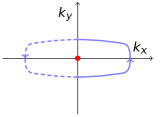
In the absence of magnetic field, the directly transmitted and twice reflected waves222Waves of multiple reflections also contribute to the Fabry-Pérot interference but are only of minor importance, even in ideally ballistic transport; see, for example, Varlet et al. (2014a). [such as the case sketched in Fig. 5(a)] interfere with each other with a kinetic phase difference (WKB standing for Wentzel-Kramers-Brillouin), which is proportional to the cavity size and the longitudinal component of the wave vector . Under the influence of an external magnetic field , the resulting Lorentz force bends the semiclassical electron trajectories, some of which form closed loops [such as the case sketched in Fig. 6(a)], wrapping finite areas and therefore an Aharanov-Bohm phase , which can be shown (when is weak) to be , where is the Fermi wave vector. At the same time, also reduces as a consequence of the bending and the conservation of , where is proportional to because of the mechanical momentum with the chosen gauge333Note that when applying the periodic boundary condition along the transverse dimension (), this gauge is practically the only choice in order to keep the system -independent Liu and Richter (2012). for . Thus the increase of leads to an increase of but decrease of , while the increase of leads to a decrease of and increase of . When measuring the conductance as a function of magnetic field and density (), the two competing phase terms result in the Fabry-Pérot interference fringes (each stripe corresponding to a constant ) dispersing with increasing towards higher density in a parabolic pattern Young and Kim (2009); Shytov et al. (2008); Ramezani Masir et al. (2010); Nam et al. (2011); Liu and Richter (2012); Rickhaus et al. (2013); Grushina et al. (2013); Masubuchi et al. (2013); Rickhaus et al. (2015); Calado et al. (2015).
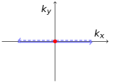
The cyclotron bending contributes to the phase in a different way. At , the trajectory propagating at normal incidence will be fully transmitted. Thus there exists no such trajectory as the one depicted in Fig. 5(a) which, in momentum space, would directly enclose the origin [see Fig. 5(b)]. In the presence of a finite (and typically weak) , however, closed loops such as that shown in Fig. 6(a) can form because of finite backscattering at oblique incidence, and the corresponding momentum-space trajectories will enclose the origin as sketched in Fig. 6(b). Due to the existence of a singularity at the -point (vertex Anandan (1992); Shytov et al. (2009)), the -Berry phase is picked up. In the measurements, this will therefore lead to a shift of the oscillation pattern by half a period. Hence this -shift constitutes a direct evidence for Klein tunneling, through the analysis of backscattering.
The observation of the phase jump has been made for SLG cavities of various qualities and widths Young and Kim (2009); Nam et al. (2011); Rickhaus et al. (2013); Grushina et al. (2013); Masubuchi et al. (2013); Rickhaus et al. (2015). In 2009, Young and Kim presented their pioneering experiment and reported on the observation of conductance oscillations in a graphene bipolar heterojunction Young and Kim (2009). The cavity was electrostatically induced by the use of a narrow top gate (), allowing for the observation of ballistic interference, as the mean free path was estimated to be larger than . The signature of Klein tunneling and of its perfect transmission was further demonstrated by investigating the magnetic field dependence of the conductance oscillations, where the -shift of the oscillations was seen. The specificity of the measured shift of the oscillations agreed with the theoretical prediction Shytov et al. (2008) and was later reproduced qualitatively Ramezani Masir et al. (2010) and quantitatively Liu and Richter (2012) by transport calculations.
In 2013, a big step was made in the quality of the produced devices. Rickhaus et al. Rickhaus et al. (2013) and Grushina et al. Grushina et al. (2013) reported on the use of local bottom gates in suspended devices to engineer smooth, electrostatically defined junctions with stunning qualities, enabling for the observation of Fabry-Pérot interference on length scales larger than Maurand et al. (2014). Once again, the characteristic Berry phase shift was present in the magnetic field data. In Ref. Rickhaus et al. (2013), the finesse of the cavity and the resulting visibility of the oscillation pattern were studied in great detail and analyzed in view of the smoothness of the electrostatic landscape.
In the case of BLG, however, the Berry phase of could not be identified in a similar way in an interferometer geometry, since a phase of is equivalent to a phase of . Until today, the only measurable contribution of this phase was observed in quantum Hall measurements, as experimentally demonstrated for the first time in Ref. Novoselov et al. (2006). Moreover, an electrostatically controlled BLG pn’p junction normally requires a dual gated cavity where the inversion symmetry is broken such that the BLG is no longer gapless. The consequence of the band gap on transport and its relation to the pseudospin are to be discussed in the following section.
III Band gap and peudospin
The pseudospin in SLG and BLG is restricted to the - plane as a consequence of the lattice inversion symmetry. If this symmetry is broken, the situation is different.
III.1 Inversion symmetry breaking
By applying a different potential to the two sublattices, the inversion symmetry can be lifted. In SLG, this can be done by aligning the flake on a hexagonal boron nitride substrate Decker et al. (2011); Yankowitz et al. (2012); Gorbachev et al. (2014); Lundeberg and Folk (2014). The closely similar lattice structure of graphene and hexagonal boron nitride (h-BN) results in locally aligning the atomic site A of graphene with a boron atom and its B site with a nitrogen atom (or vice-versa). The two carbon sites therefore experience different potentials, leading to the broken inversion symmetry. In BLG, setting the two layers to different potentials, using for example external gates McCann and Fal’ko (2006); McCann (2006); McCann et al. (2007); Mucha-Kruczyński et al. (2009), also breaks the inversion symmetry. The experimental realization of the BLG symmetry breaking will be treated in more detail in Section IV.
With the inversion asymmetry, the resulting Hamiltonians are generalized from Eq. (2) to the form
| (9) |
where is the asymmetry parameter McCann and Fal’ko (2006).
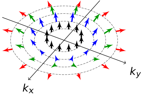
One observes in Eq. (9) that adding an asymmetry adds diagonal terms to the Hamiltonians, i.e. a -component, which gives rise to a -component of the polarization vector itself. In this situation, the pseudospin is not bound to the equatorial plane any more. This is shown schematically in Fig. 7(a) for the case of the conduction band of SLG at the valley . We see that for small momenta (i.e. small energies, close to the band gap), the pseudospin points completely out of plane (black arrows). On the Bloch sphere, this means that the pseudospin stays aligned with the -axis and therefore encloses no area, giving rise to a zero Berry phase. This is shown in Fig. 7(b) with the black needle. The chirality is broken. Moving towards higher energies, the pseudospin tends to asymptotically recover its in-plane motion [red arrows in Fig. 7(a) and red needles in Fig. 7(e)] and therefore a -Berry phase. The chirality is slowly restored Lundeberg and Folk (2014). In-between the two extreme cases, the pseudospin is partially -polarized, leading to a Berry phase varying between and , as shown with the blue and green arrows in Fig. 7(a) and the blue and green needles in Fig. 7(c)–(d).
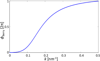
Exactly the same happens with BLG when a band gap is opened. Close to the edges of the valence or conduction band, the pseudospin is fully -polarized, leading to a Berry phase of Li et al. (2012). When the energy increases, the chirality is slowly restored, until the pseudospin returns to the -plane and the Berry phase is set back to . This is illustrated in Fig. 8, where the Berry phase is calculated as a function of momentum (which can be translated into an energy), and will be further explained and investigated in Section IV.
III.2 Gapped BLG pn junction
We next focus on the effect of the broken chirality induced by opening the band gap on the transmission probability of an electron wave incident on a BLG pn junction. As illustrated earlier, the perfect reflection across a bipolar potential step in BLG is expected Katsnelson et al. (2006) for pristine BLG in the absence of the band gap. However, only limited literature exists addressing the question of the effect of a gap on the tunneling properties (see, for example, Refs. Park and Sim (2011); Gu et al. (2011)). Using the same method as Ref. Liu et al. (2012), we apply the Green’s function method based on a tight-binding model associated with the periodic Bloch phase to illustrate the influence of the asymmetry on the angle-resolved transmission . This asymmetry results in opening a band gap in the band structure of BLG McCann and Fal’ko (2006); McCann (2006); McCann et al. (2007); Mucha-Kruczyński et al. (2009).
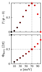
We consider transport through an ideally sharp np junction444Note that an atomically sharp np junction is expected to induce intervalley scattering, which is not our main focus here. Numerically, such scattering leads to imperfection of at for the case of SLG, and for the case of BLG with , as can be noted in Fig. 9(a); see the curve marked by . with a step height of at fixed Fermi energy as shown in the top panel of Fig. 9(a), where the asymmetry parameter is varied from (black curves) to (red curves). The resulting curves for various values of in this range are shown in the bottom panel of Fig. 9(a), where one observes that the transmission function changes drastically. Starting from [black curve with ], we observe that increasing breaks the anti-Klein tunneling, and increases slowly, until reaching perfect transmission at normal incidence (curve marked by ). The values and the corresponding Berry phase as a function of are respectively shown in the top and bottom panel of Fig. 9(b), where and matching each other at can be seen. This implies that, under certain circumstances, a revival of the Klein tunneling in BLG is possible, by manipulating the gap-controlled Berry phase.
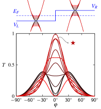
By further increasing , the Berry phase continues to increase toward while the normal incident transmission decreases rapidly toward zero, until the anti-Klein tunneling behavior is recovered. In view of the transition shown and discussed above, the strength of BLG lies in the following fact: the tunability of bilayer graphene allows not only to conveniently open (and control) a band gap in its dispersion, but also to tune its chirality, enabling a possible switching between BLG-like and SLG-like transport characteristics. In the following, we present an experiment illustrating how the chirality in a gapped BLG system can be broken.
IV Interference experiment with gapped BLG
As mentioned earlier in Sec. II.3, there is no report in the literature showing explicit signatures of the -Berry phase in BLG interferometers, as there is in SLG. However, as described in the previous section, once a band gap is opened, the chirality of BLG is changed and a finite transmission at normal incidence, associated to a finite Berry phase, occurs. In the following, we investigate the chiral properties of BLG via measurements performed on a dual-gated BLG Fabry-Pérot (FP) interferometer. Parts of the data presented below were published in Ref. Varlet et al. (2014a).
IV.1 Gate-tunable BLG interferometer
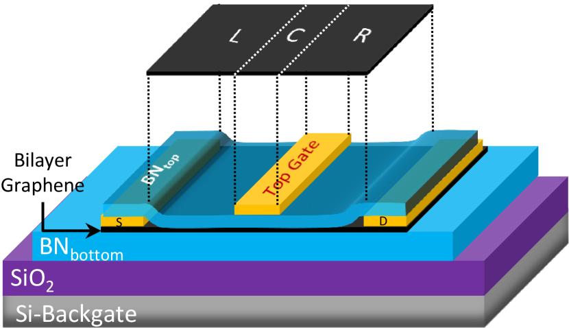
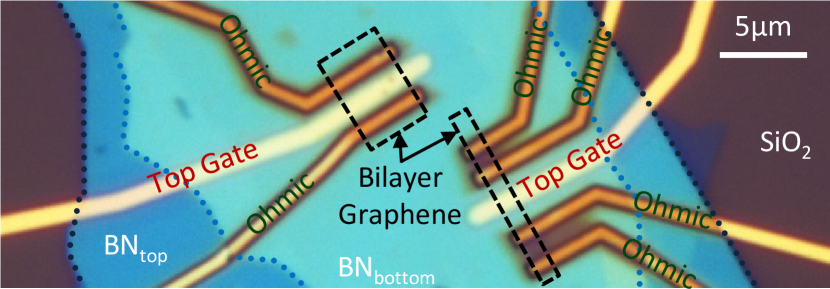
The device under investigation is sketched in Fig. 10(a) and (b) (right device). It consists of a h-BN/BLG/h-BN stack which is deposited on a Si/SiO2-substrate, prepared as described in Ref. Varlet et al. (2014b). The stack was realized using the dry transfer technique pioneered in Ref. Dean et al. (2010).
For such a geometry, the silicon backgate allows us to tune the whole BLG stripe, whereas the local top gate acts only on the central region underneath. The device therefore consists of three areas in series, as shown in Fig. 10(a): the two outer regions (labeled L and R) are simultaneously tuned by the backgate voltage , and the central area (labeled C) is under the influence of both and the topgate voltage . The geometry is the following: the width of the whole flake is , and the lengths of the three regions are and .
In the following, the sample is placed in a variable temperature inset at temperature . We apply a constant symmetric bias voltage between the Ohmic contacts [labeled S and D in Fig. 10(a)] and record the current, allowing to measure the conductance . Additionally, the top gate voltage is modulated with a small AC voltage, which enables the measurement of the normalized transconductance .
IV.2 Basic transport characterization
The measurement of such a dual-gated device is shown in Fig. 11(a), where the conductance is displayed as a function of both and . Depending on the applied voltages, the polarity of the outer regions and of the central one can be changed, from hole-like to electron-like transport. This gives rise to four different polarity combinations: two of them exhibit the same polarity in the three regions (pp’p and nn’n – the prime referring to the central region C) and the other two exhibit opposite polarity (np’n and pn’p). The charge neutrality of the two outer regions is apparent from the two horizontal blue lines in the middle of Fig. 11(a) and the charge neutrality in the dual-gated region occurs along the diagonal blue line. The latter spans along the so-called displacement field D axis, as indicated in the figure. While increasing , towards one corner of the map or the other, the conductance at the charge neutrality point decreases towards zero. This insulating state is due to the band gap being opened while the asymmetry between the top- and bottom layer of the BLG flake is made larger. Along the D-axis, the Fermi energy within the dual-gated region lies in the middle of the gap and the density is equal to zero. As reported in various experiments Oostinga et al. (2008); Russo et al. (2009); Weitz et al. (2010); Taychatanapat and Jarillo-Herrero (2010); Shimazaki et al. (2015); Sui et al. (2015), hopping processes resulting from residual disorder were found to be the dominant transport mechanism in this regime and at such low temperatures.
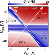
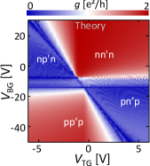
In order to capture the electrostatic picture of the device and to reproduce our observations, we implemented the following model. First, the density in each of the three areas – L, C and R – was related to the applied gate voltages and via the use of a parallel plate capacitor model. Each area density is separated into three terms: the bottom graphene sheet density, the top graphene sheet density and the intrinsic doping of the area, which is directly estimated from the measured data. Following McCann McCann and Koshino (2013), the asymmetry parameter is calculated in each region. With the knowledge of and , the band offset is finally calculated and inserted in the nearest-neighbor tight-binding Hamiltonian of BLG Slonczewski and Weiss (1958); McClure (1957). The details of the calculations are explained in Ref. Varlet et al. (2014a). As a last step, the resulting energy profile is used to calculate the conductance through the device as a function of the applied gate voltages. This uses a Green’s function formalism similar to Refs. Liu and Richter (2012); Rickhaus et al. (2013). Here, only the C region is considered as the scattering region, L and R being treated as semi-infinite leads. As shown in Fig. 11(b), which displays the normalized conductance (no mode counting implemented so that its maximum is due to the valley degeneracy of the spin-independent calculation), the overall electrostatic picture is very well captured by the model.
IV.3 Interference pattern
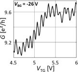
As shown in Fig. 12(a), an oscillating conductance is observed in the pn’p bipolar regime. To increase the visibility of the oscillations, one looks at the corresponding transconductance map, recorded simultaneously and shown in Fig. 12(b). Cuts within these two maps are shown in Fig. 12(c)–(d). They allow to better see the strength of the oscillating pattern. In the following, we focus on the transconductance signal to analyze the oscillatory pattern in more detail. However, the same study could be carried out utilizing the conductance.
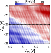
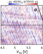
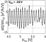
As highlighted in Fig. 12(b), the oscillations evolve parallel to the D-axis (the slope of the D-axis is displayed as a black line labeled ). This indicates that they arise from a mechanism taking place in the dual-gated part of the device. To confirm the ballistic origin of the observed signal, the frequency of the oscillations was analyzed. To do so, each top gate voltage point was converted into a density and then into a wavevector. Performing a discrete Fourier transform, we found that the oscillation frequency was . This confirmed that the main contribution to the phase arises from interference between a directly transmitted wave and a wave which is transmitted through the cavity after bouncing once back and forth in the cavity. This corresponds to a phase difference , with a frequency . With this frequency analysis, we convince ourselves that the observation is related to ballistic transport in the dual-gated region, leading to a clear FP interference pattern.
IV.4 Broken or not broken?
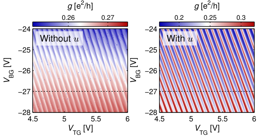
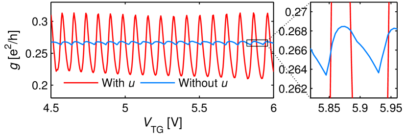
From the previous analysis, a question remains to be explored: does the band gap play a role in our experimental observation? To elucidate this question, we first compare the measured oscillations shown in Fig. 12(b) with the theoretical predictions for two different systems: on one hand, a BLG system where the asymmetry between the layer is ignored is considered (i.e. the process of band gap opening is ignored and the gates are only responsible for tuning the overall sheet density) and, on the other hand, the same calculation method as already implemented in Fig. 11(b) is used, which follows McCann’s model McCann and Koshino (2013) and takes into account the asymmetry. The results of both calculations are shown in Fig. 13(a)–(b). Qualitatively, we observe that the shape of the oscillations is very different: in Fig. 13(a) (left panel), the oscillations appear very sharp and asymmetric, which is not the case in right panel, where the oscillations appear more symmetric, almost like a sine function [also visible in Fig. 13(b)]. Similar observations were made in Ref. Gu et al. (2011). Comparing these maps with the measurement data shown in Fig. 12(b), we conclude that our observation is qualitatively closer to the case where the band gap is implemented.
Another confirmation lies in the visibility of the interference pattern. The visibility of the measured conductance oscillations is found to be . In a fully ballistic situation as those shown in Fig. 13(a)–(b), the visibility of the calculated conductance yields for the case where is implemented and when is set to zero. However, the assumption of a fully ballistic device has to be weakened. Indeed, by comparing the maps shown in Fig. 12 and Fig. 13, one can see that the measurement signal exhibits imperfections. We would therefore expect the theoretical visibility values to be upper bounds compared to the experimental signal. We therefore conclude that the value provided by the non-gapped case is inappropriate to describe our observation, pointing towards a role played by the band gap on our ballistic interference signatures.
IV.5 Gate-tunable Berry phase
As explained in Section III, signatures of the broken chirality due to band gap opening should appear in the Berry phase, which varies as a function of the induced asymmetry and might be accessible in experiments. To find this out, the oscillations have to be investigated at varying magnetic field.
Based on the phase difference between a transmitted and a twice reflected electron wave, the FP resonance condition is
| (10) |
As explained earlier in Sec. II.3, and are magnetic-field-dependent and are the origin of the parabolic trend of the oscillations evolving as a function of . What strongly differs from the previously mentioned case of SLG is the Berry phase. In SLG, due to perfect transmission at normal incidence, the system requires finite magnetic field to build up trajectories which, in momentum space, enclose the origin and therefore pick up the Berry phase. In the case of gapped BLG, since even at the normal incident transmission is finite (in the studied energy range with finite ), there already exist trajectories which go through , implying that the Berry phase is already involved.555Recall the trajectories sketched in Fig. 5, which do not exist in the case of SLG due to the Klein tunneling. Here for gapped BLG, due to finite transmission and reflection at normal incidence, such trajectories do exist, so that the origin is always enclosed, independent of . The Berry phase therefore does not depend on the magnetic field Varlet et al. (2014a), but only on the asymmetry .
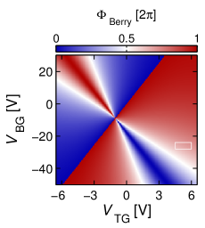
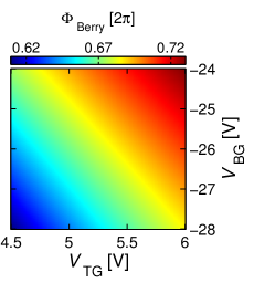
Figure 14(a) shows the predicted Berry phase of the dual-gated region of the device in the range of voltages available. We see that the Berry phase varies from to in this map, and especially involves the value (white area), which is characteristic of SLG. However, since the interference is only visible in a limited range of gate voltage (white square marked in the map), we cannot probe the dramatic change of the Berry phase value. The values taken by the Berry phase in the region of interest are shown in Fig. 14(b). We see that the Berry phase evolves, from to and is not constant. The limited evolution leads to only very small offsets of the oscillations as a function of top gate voltage, such that it is not visible in the experimental data. Further investigations would be required to probe the effect of the Berry phase, ideally with oscillations visible in a broader range of gate voltages.
Moreover, turning a BLG into a SLG-like by manipulating the gap and hence the Berry phase is theoretically possible, as shown in Section III. This would however require a system with three cavities, each being dual-gated. Additionally, the probing regime would have to cover the Berry phase of (which is supposed to be close to the gap). This would constitute one big step beyond the above-presented experiment where only one dual-gated region was designed.
V Conclusion and outlook: experiments based on the broken chirality
We have explored theoretically the chirality of charge carriers both in SLG and BLG. We pointed out experimental realizations of FP interferometers which allow, in the SLG case, to directly probe the key parameter which is the Berry phase. We next focused on single- and bilayer graphene systems in which the inversion symmetry is lifted. Such systems exhibit band gaps in their band structure. Close to the edge of the gap, the pseudospin is found to be fully -polarized, indicating a broken chirality, which is then restored going away from the gap. This is associated with a Berry phase varying from zero to its pristine value ( for SLG or for BLG). Finally, we focused on the breaking of the chirality in BLG. Beyond the tunability of the anti-Klein tunneling, one of the key results is that the physics of BLG can mimic the behavior of SLG as the tunability of the transmission function allows to recover a perfect transmission at normal incidence for a certain energy range, together with a Berry phase of , characteristic of the Klein tunneling in single-layer graphene. We presented an experiment on a dual-gated BLG graphene device where Fabry-Pérot interference were probed, indicating ballistic transport. This allowed to illustrate the chirality breaking in more detail.
Very recently, experimentalists have been able to use the pseudospin degree of freedom both in SLG and in BLG. In 2014, Gorbachev et al. Gorbachev et al. (2014) demonstrated the generation of topological currents in a SLG system with broken inversion symmetry. To do so, they aligned the graphene flake on a hexagonal boron nitride substrate, inducing an imbalance between the A and B atomic sites. Because graphene has two valleys, a broken inversion symmetry results in the creation of topological currents with different signs in each valley. This was confirmed by the observation of a non-local signal, as strong as the applied current and at micron distances from its path. The same was observed in a similar geometry in dual-gated BLG Shimazaki et al. (2015); Sui et al. (2015). This time, dual-gating was responsible for breaking the inversion symmetry. A non-local resistance was measured, surviving up to high temperatures. Such advances in the control of the pseudospin degree of freedom are very appealing for possible applications in quantum computation, which require non-dissipative currents.
Aknowledgements
We thank M. Eich, H. Overweg, and V. Krückl for constructive comments and fruitful discussions. We also acknowledge financial support from the Marie Curie ITNs NANO and QNET, together with the Swiss National Science Foundation via NCCR Quantum Science and Technology, the Graphene Flagship and the Deutsche Forschungsgemeinschaft within SFB 689.
References
- Novoselov et al. (2004) K. S. Novoselov, A. K. Geim, S. Morozov, D. Jiang, Y. Zhang, S. Dubonos, I. Grigorieva, and A. Firsov, Science 306, 666 (2004).
- Wallace (1947) P. R. Wallace, Physical Review 71, 622 (1947).
- Novoselov et al. (2005) K. Novoselov, A. K. Geim, S. Morozov, D. Jiang, M. K. I. Grigorieva, S. Dubonos, and A. Firsov, Nature 438, 197 (2005).
- Zhang et al. (2005) Y. Zhang, Y.-W. Tan, H. L. Stormer, and P. Kim, Nature 438, 201 (2005).
- Katsnelson et al. (2006) M. I. Katsnelson, K. S. Novoselov, and A. K. Geim, Nature Physics 2, 620 (2006).
- Young and Kim (2009) A. F. Young and P. Kim, Nature Physics 5, 222 (2009).
- Klein (1929) O. Klein, Zeitschrift für Physik 53, 157 (1929).
- Novoselov et al. (2006) K. S. Novoselov, E. McCann, S. V. Morozov, V. I. Fal’ko, M. I. Katsnelson, U. Zeitler, D. Jiang, F. Schedin, and A. K. Geim, Nature Physics 2, 177 (2006).
- Slonczewski and Weiss (1958) J. C. Slonczewski and P. R. Weiss, Phys. Rev. 109, 272 (1958).
- DiVincenzo and Mele (1984) D. P. DiVincenzo and E. J. Mele, Phys. Rev. B 29, 1685 (1984).
- Ihn (2010) T. Ihn, Semiconductor Nanostructures: Quantum States and Electronic Transport (OUP Oxford, 2010).
- Bloch (1946) F. Bloch, Phys. Rev. 70, 460 (1946).
- Haldane (1988) F. D. M. Haldane, Phys. Rev. Lett. 61, 2015 (1988).
- Berry (1984) M. V. Berry, Proc. R. Soc. Lond. A 392, 45 (1984).
- Anandan (1992) J. Anandan, Nature 360, 307 (1992).
- Xiao et al. (2010) D. Xiao, M.-C. Chang, and Q. Niu, Rev. Mod. Phys. 82, 1959 (2010).
- Park and Sim (2011) S. Park and H.-S. Sim, Phys. Rev. B 84, 235432 (2011).
- McCann and Koshino (2013) E. McCann and M. Koshino, Reports on Progress in Physics 76, 056503 (2013).
- Tudorovskiy et al. (2012) T. Tudorovskiy, K. J. A. Reijnders, and M. I. Katsnelson, Physica Scripta T146 (2012), 10.1088/0031-8949/2012/T146/014010.
- Liu et al. (2012) M.-H. Liu, J. Bundesmann, and K. Richter, Phys. Rev. B 85, 085406 (2012).
- Sutar et al. (2012) S. Sutar, E. S. Comfort, J. Liu, T. Taniguchi, K. Watanabe, and J. U. Lee, Nano Letters 12, 4460 (2012), pMID: 22873738.
- Rahman et al. (2015) A. Rahman, J. W. Guikema, N. M. Hassan, and N. Marković, Appl. Phys. Lett. 106, 013112 (2015).
- Shytov et al. (2008) A. V. Shytov, M. S. Rudner, and L. S. Levitov, Phys. Rev. Lett. 101, 156804 (2008).
- Varlet et al. (2014a) A. Varlet, M.-H. Liu, V. Krueckl, D. Bischoff, P. Simonet, K. Watanabe, T. Taniguchi, K. Richter, K. Ensslin, and T. Ihn, Phys. Rev. Lett. 113, 116601 (2014a).
- Liu and Richter (2012) M.-H. Liu and K. Richter, Phys. Rev. B 86, 115455 (2012).
- Ramezani Masir et al. (2010) M. Ramezani Masir, P. Vasilopoulos, and F. M. Peeters, Phys. Rev. B 82, 115417 (2010).
- Nam et al. (2011) S.-G. Nam, D.-K. Ki, J. W. Park, Y. Kim, J. S. Kim, and H.-J. Lee, Nanotechnology 22, 415203 (2011).
- Rickhaus et al. (2013) P. Rickhaus, R. Maurand, M.-H. Liu, M. Weiss, K. Richter, and C. Schönenberger, Nature Communications 4 (2013), 10.1038/ncomms3342.
- Grushina et al. (2013) A. L. Grushina, D.-K. Ki, and A. F. Morpurgo, Applied Physics Letters 102, 223102 (2013).
- Masubuchi et al. (2013) S. Masubuchi, S. Morikawa, M. Onuki, K. Iguchi, K. Watanabe, T. Taniguchi, and T. Machida, Japanese Journal of Applied Physics 52, 110105 (2013).
- Rickhaus et al. (2015) P. Rickhaus, P. Makk, M.-H. Liu, E. Tóvári, M. Weiss, R. Maurand, K. Richter, and C. Schönenberger, Nature Communications 6, 6470 (2015).
- Calado et al. (2015) V. E. Calado, S. Goswami, G. Nanda, M. Diez, A. R. Akhmerov, K. Watanabe, T. Taniguchi, T. M. Klapwijk, and L. M. Vandersypen, arXiv preprint arXiv:1501.06817 (2015).
- Shytov et al. (2009) A. Shytov, M. Rudner, N. Gu, M. Katsnelson, and L. Levitov, Solid State Comm. 149, 1087 (2009).
- Maurand et al. (2014) R. Maurand, P. Rickhaus, P. Makk, S. Hess, E. Tóvári, C. Handschin, M. Weiss, and C. Schönenberger, Carbon 79, 486 (2014).
- Decker et al. (2011) R. Decker, Y. Wang, V. W. Brar, W. Regan, H.-Z. Tsai, Q. Wu, W. Gannett, A. Zettl, and M. F. Crommie, Nano Letters 11, 2291 (2011).
- Yankowitz et al. (2012) M. Yankowitz, J. Xue, D. Cormode, J. D. Sanchez-Yamagishi, K. Watanabe, T. Taniguchi, P. Jarillo-Herrero, P. Jacquod, and B. J. LeRoy, Nat Phys 8, 382 (2012).
- Gorbachev et al. (2014) R. V. Gorbachev, J. C. W. Song, G. L. Yu, A. V. Kretinin, F. Withers, Y. Cao, A. Mishchenko, I. V. Grigorieva, K. S. Novoselov, L. S. Levitov, and A. K. Geim, Science 346, 448 (2014).
- Lundeberg and Folk (2014) M. B. Lundeberg and J. A. Folk, Science 346, 422 (2014).
- McCann and Fal’ko (2006) E. McCann and V. I. Fal’ko, Physical Review Letters 96, 086805 (2006).
- McCann (2006) E. McCann, Physical Review B 74, 161403 (2006).
- McCann et al. (2007) E. McCann, D. Abergel, and V. Fal’ko, Solid State Communications 143, 110 (2007).
- Mucha-Kruczyński et al. (2009) M. Mucha-Kruczyński, E. McCann, and V. I. Fal’ko, Solid State Communications 149, 1111 (2009).
- Li et al. (2012) J. Li, I. Martin, M. Büttiker, and A. F. Morpurgo, Physica Scripta 2012, 014021 (2012).
- Gu et al. (2011) N. Gu, M. Rudner, and L. Levitov, Phys. Rev. Lett. 107, 156603 (2011).
- Varlet et al. (2014b) A. Varlet, D. Bischoff, P. Simonet, K. Watanabe, T. Taniguchi, T. Ihn, K. Ensslin, M. Mucha-Kruczyński, and V. Fal’ko, Phys. Rev. Lett. 113, 116602 (2014b).
- Dean et al. (2010) C. R. Dean, A. F. Young, I. Meric, C. Lee, L. Wang, S. Sorgenfrei, K. Watanabe, T. Taniguchi, P. Kim, K. L. Shepard, and J. Hone, Nature Nanotechn. 5, 722 (2010).
- Oostinga et al. (2008) J. B. Oostinga, H. B. Heersche, X. Liu, A. F. Morpurgo, and L. M. K. Vandersypen, Nature Materials 7, 151 (2008).
- Russo et al. (2009) S. Russo, M. F. Craciun, M. Yamamoto, S. Tarucha, and A. F. Morpurgo, New J. Phys. 11 (2009), 10.1088/1367-2630/11/9/095018.
- Weitz et al. (2010) R. T. Weitz, M. T. Allen, B. E. Feldman, J. Martin, and A. Yacoby, Science 330, 812 (2010).
- Taychatanapat and Jarillo-Herrero (2010) T. Taychatanapat and P. Jarillo-Herrero, Phys. Rev. Lett. 105, 166601 (2010).
- Shimazaki et al. (2015) Y. Shimazaki, M. Yamamoto, I. V. Borzenets, K. Watanabe, T. Taniguchi, and S. Tarucha, arXiv preprint arXiv:1501.04776 (2015).
- Sui et al. (2015) M. Sui, G. Chen, L. Ma, W. Shan, D. Tian, K. Watanabe, T. Taniguchi, X. Jin, W. Yao, D. Xiao, et al., arXiv preprint arXiv:1501.04685 (2015).
- McClure (1957) J. W. McClure, Phys. Rev. 108, 612 (1957).