Scanning Kerr microscopy study of current induced switching in Ta/CoFeB/MgO films with perpendicular magnetic anisotropy
Abstract
Ta/CoFeB/MgO trilayers with perpendicular magnetic anisotropy are expected to play a key role in the next generation of current and electric field switched memory and logic devices. In this study we combine scanning Kerr microscopy with electrical transport measurements to gain insight into the underlying mechanisms of current induced switching within such devices. We find switching to be a stochastic, domain wall driven process, the speed of which is strongly dependent on the switching current. Kerr imaging shows domain nucleation at one edge of the device which modelling reveals is likely assisted by the out-of-plane component of the Oersted field. Further domain growth, leading to magnetisation reversal, may still be dominated by spin torques.
pacs:
Valid PACS appear hereI Introduction
The ever growing demand for higher density storage and faster processing speeds has led to great advances in the field of data storage in the last few decadesBandic2008 . The discovery of tunnelling magnetoresistance (TMR) has made the magnetic tunnel junction (MTJ) one of the leading candidates for next generation high density magnetic random access memory (MRAM).
Traditional MTJ memory requires an external magnetic field, generated by a current, to induce switching during the read/write procedure. Recently there has been great interest in switching the memory bit directly by using spin transfer torques (STT) generated by charge currents. Conventional STT switching requires current to be injected directly through a tunnel barrier but recent studies have utilised the torques generated by spin Hall and Rashba effects to switch elements with an in plane current. To date these phenomena have been investigated mostly in layered structures containing HM/FM/Ox sub-units in which the ferromagnetic (FM) layer is sandwiched between a heavy metal (HM) and an oxide (Ox). Spin-transfer torque magnetic random-access memory (STT-MRAM), has been explored as a viable option to replace dynamic random access memory (DRAM) and may provide performance comparable to DRAM main memory with an average 60% reduction in main memory energyKultursay2013 . With main memory energy now accounting for as much as 30% of overall system power Carter2010 ; Hoelzle2009 STT-MRAM has the potential to significantly reduce the operational cost of computing systems.
It has been demonstrated that the Ta/CoFeB/MgO sub-unit could fulfil the three criteria required for high performance MTJs for STT-MRAM, namely high tunnelling magnetoresistance (TMR), low switching current, and high thermal stability for small device dimensions. With TMR ratios of 120% in Ta/MgO/CoFeB/MgO/CoFeB/TaIkeda2010 stacks and 162% in similar stacks with Mo layersAlmasi2015 , along with switching currents of A/cm2 for similar devicesQiu2014 ; Zhang2014 , and good thermal stability for devices with nm diameterIkeda2010 , Ta/CoFeB/MgO is indeed a viable candidate for next generation STT-MRAM.
A deeper understanding of the underlying switching mechanisms is critical for effective device fabrication and has recently been the subject of much debate. Kim et alKim2013 report a strong HM and FM thickness dependence of both the Rashba spin orbit field and the spin Hall torques. Torrejon et alTorrejon2014 also report a strong thickness dependence of their relative contributions to the switching, with spin Hall torque dominating for thicker HM underlayers. The relative contributions made by these effects are also influenced by capping layer thicknessQiu2013 and temperatureQiu2014 . In this study we combine scanning Kerr imaging with electrical transport measurements to gain further insight into the switching process.
II Experimental
II.1 Fabrication Details
We focus only on CoFeB with the composition Co40Fe40B20 in which perpendicular magnetic anisotropy (PMA) was been achieved through thermal annealing. Stacks of Ta(4 nm)/CoFeB(1 nm)/MgO(1.6 nm)/Ta(1 nm) were sequentially deposited on thermally oxidised Si wafers in a high vacuum magnetron sputtering system. Further details of this process can be found in ref. (12). The 1 nm Ta layer was used as a capping layer to prevent atmospheric oxidisation.
The stacks were patterned into Hall bars (20 x 140 m2) (Fig.1.(d)) using photolithography. After stack deposition a second round of photolithography and a Au deposition was used to define contact pads. Au contacts were not critical for switching but allow wire-bonding to facilitate electrical measurements.
The sample was then annealed in vacuum (1 x 10⁻⁶ Torr) at for 1 hour with 2 hours of ramping up and 6 hours of natural cooling under a magnetic field of 0.45 T perpendicular to the plane of the sample. It was shown by several groupsHao2015 ; Worledge2011 ; Avci2014 that the annealing temperature is critical for the formation of robust PMA. As-prepared samples do not support PMA as they have sharp, but disordered, interfaces while at high annealing temperatures (>) diffusion within the interfacial region is detrimental to the PMA.
II.2 Measurement Details
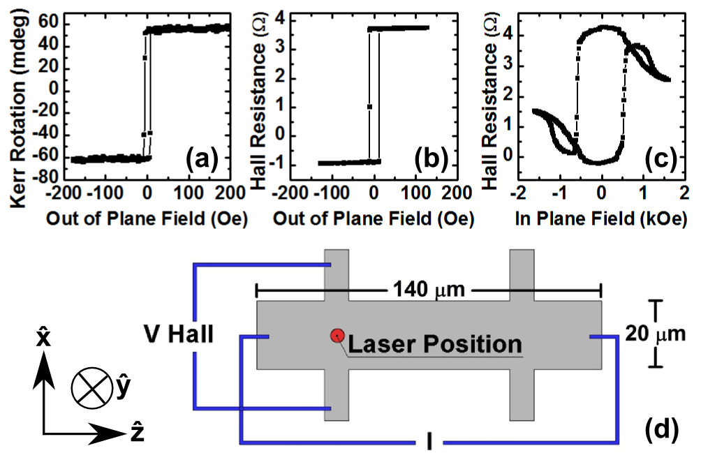
For magnetotransport measurements wire-bonding was used to connect the Hall bar to two 50 coplanar waveguides (CPWs). A current was applied along the direction parallel to the long edge of the Hall bar () and the Hall resistance was measured across the contacts perpendicular to the current () as shown in Fig.1.(d). In this way the magnetization between the contact pads was probed via the anomalous Hall effect (AHE). The Hall bar and CPWs were placed in a scanning Kerr microscope so that the magnetisation within a sub-micron region could be probed via the magneto-optical Kerr effect (MOKE), simultaneously with the Hall resistance measurements. The MOKE measurement was performed by focusing the beam from a 633 nm He-Ne laser onto the sample surface with a 40X objective lens, and recording the optical rotation of the back-reflected beam using a simple optical bridge detector. In each experiment a large in plane field was used to set the initial perpendicular magnetisation direction. The direction of the magnetisation was reproducible due to a slight () tilt of the applied field relative to the plane of the Hall bar. The field was then reduced to remanence ( Oe) along the direction of current flow, as shown in Fig.1.(c). All measurements were performed at room temperature.
III Results and Discussion
Using an out-of-plane () field the saturation Kerr rotation (Fig.1.(a)) and Hall resistance (Fig.1.(b)) were found for each of the bistable out-of-plane magnetisation M states. These results were used to confirm full magnetization reversal had occurred in subsequent current induced switching experiments. The devices showed a particularly low ( 10 Oe) perpendicular coercive field. The Hall resistance for the in-plane field used to set the initial M state is shown in Fig.1.(c).
III.1 Time resolved - time-dependent current
In the magnetotransport measurements shown in Fig.2.(a) the initial magnetisation state (M-) was measured with a small D.C. current mA and was found to correspond to a Hall resistance of . The magnetization was switched towards the opposite bistable state (M+), which corresponds to a Hall resistance of , by current pulses mA with a duration of s. was then applied once more to measure the final magnetisation state. Throughout this process the Kerr rotation (Fig.2.(b)) was continuously monitored at a position mid-way between the Hall contacts shown in Fig.1.(d).
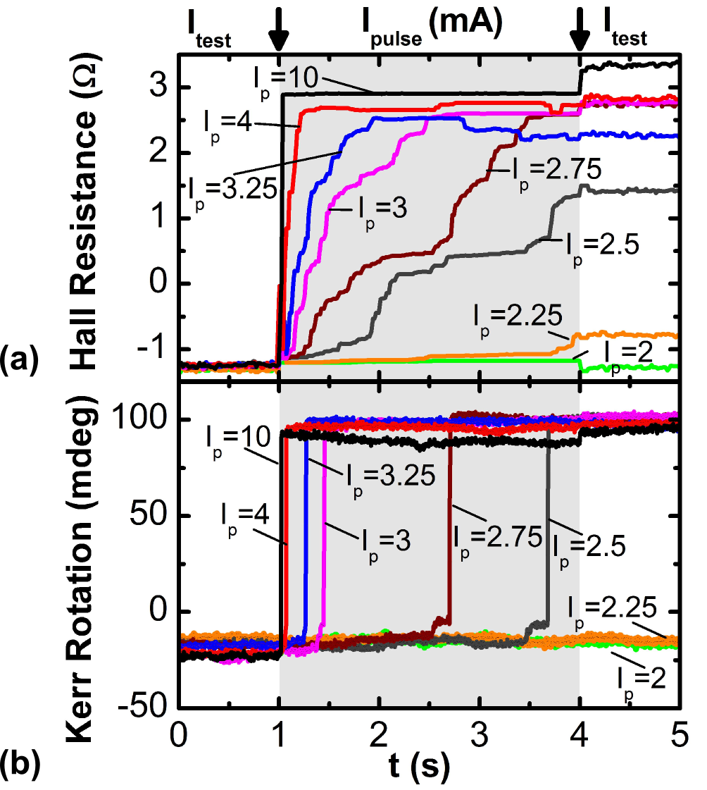
For mA, switching occurred on a timescale < 1 s, faster than the resolution of the measurement technique. By reducing the pulsed current to the range mA switching occurs considerably more slowly allowing the change in Hall resistance to be easily observed within the s pulse duration. Due to the strong PMA, an intermediate Hall resistance value corresponds to a domain state in which the magnetisation points either in to or out of the plane. The intermediate Hall resistance is effectively equivalent to a line integral of all M states between the contact pads. This is confirmed by the Kerr rotation shown in Fig.2.(b) where the local M switches instantaneously between the two states. Switching in Fig.2.(b) coincides with large steps in the Hall resistance, which are most clear for currents in the range mA. This implies that a large area (length equal to a few m) switches simultaneously. Whether the switching is due to a single domain or a collection of smaller domains is difficult to determine as for and mA a small step before full switching can be seen in the Kerr rotation (Fig.2.(b)). This must be due to either the full switching of a small domain, less than the size of the laser spot, or else the laser has been positioned on a domain wall at the upper edge of a larger domain. For the highest currents (seen for mA in Fig.2.(a)), the final Hall resistance is slightly larger than that observed for lower currents. This is likely due to the magnetization of the contact pad regions being more strongly pinned and requiring higher currents to switch than the body of the device. For higher currents (again seen clearly for mA) the Hall resistance shows full switching occurs within the first s but the final Hall resistance measured with is larger than the Hall resistance measured during the pulse. This behaviour may be due to the perpendicular component of the Oersted field (in the direction) opposing reversal on one edge of the device during . This field will be significantly lower during , when full reversal finally occurs. The role of the Oersted field will be discussed further in the final section of this paper. For the lowest currents mA no switching occurs, which allows us to calculate the critical switching current for this device. The switching process is stochastic in nature as shown in Fig.3 so an average of repeated measurements gave mA. Many comparable studies attribute switching purely to the giant spin Hall effect and so calculate critical current densities from only the current in the Ta layer. Based on typical resistivities of cm and cm Hao2015 , of the current flows in the Ta layer. This gives mA and a critical current density of A/cm2. In stochastic systems critical parameter values depend upon both temperature and the characteristic measurement time however it is still worthwhile to compare this critical current density to similar studiesQiu2014 ; Zhang2014 which report critical densities of A/cm2. The critical switching current for this PMA device is comparable to those reported for the better established in plane MTJsIkeda2007 and giant magnetoresistance (GMR) spin-valve sensorsLacour2004 . Our experiment not only demonstrates the strong dependence of the switching speed on but also highlights the need for careful consideration of current sweep rates when extracting . Close to partial switching can occur, which may artificially lower values extracted from swept current experiments in which M is not reset between incremental increased of the current values.
III.2 Time resolved - constant current
During the experiments in which was varied, the Hall resistance trace and the time of switching observed in the Kerr signal were not always the same for repeated switching measurements made with identical . Fig.3 highlights the stochastic nature of this process showing switching processes under nominally identical conditions for mA. The parameters for this experiment were identical to those discussed for Fig.2 but the pulse length was increased to s so that full switching could be obtained within the duration of the pulse at a lower value.
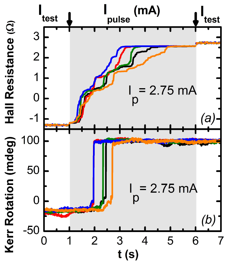
In the transport measurements shown in Fig.3.(a) the Hall resistance is similar in each event for the first s of the pulse. The Hall resistance then diverges between s before reaching the same saturation state in the final s. The divergence coincides with a large step in the Hall resistance which occurs at the same time as the large change in Kerr rotation seen in Fig.3.(b). As the Kerr rotation probes only the center of the device (Fig.1.(d)), it can be inferred that for the first s of the pulse, domains at the edges of the Hall bar switch more easily than the magnetisation at its center, and that switching follows a similar ’path’ in each event (reasons for this are to be discussed and shown in Fig.5). The switching of the central region, observed as a large step in Hall resistance and change in Kerr rotation, occurs later in the pulse and appears more random than the switching of the edge of the device.
III.3 Static imaging during current induced switching
For further insight into the domain configuration during switching, scanning MOKE images were acquired for a series of stable (on the timescale of the imaging experiment) domain configurations during the switching process. Fig.4.(a) shows the Hall resistance values at which the images (b) to (h) were taken. It was not feasible to image a single switching event as the ’mid’ states (with M close to 50/50 in and out of plane) were unstable over the imaging time (several hours). Images were instead taken on either side of this unstable middle region for the two separate partial switching events shown in Fig.4.(a).
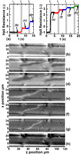
Fig.4.(b) shows M- corresponding to a Hall resistance of . As is applied we observe the formation (c) and growth (d) of large domains of M+. These domains appear to grow from the edge of the Hall bar and remain pinned at more than one site (e.g. z m x m). For the second set of stable states the majority of M lies in the M+ direction. The large reversed domain seen in (e) is in a similar position to the domain seen in (c) and (d) and also appears pinned at the same site. This domain then shrinks in (f) and (g) whilst remaining pinned until a full reversal to M+ is observed in (h).
Reverse domains appear to form first at the edge of the device, as observed in (b) to (d) where the domain forms at the edge (x m), and then grows towards the center. When reversal is close to completion the largest portion of the original domain state appears to be located on the opposite edge of the device, as seen clearly in (e) around x = m. This may again be due to the presence of the Oersted field, with the component of this field () having peak magnitude but opposite polarity at the long edges of the device.
III.4 Modelling the Oersted field
Many studies of similar structures do not discuss the presence of Oersted fields. Some studiesLiu2012b ; Yu2014 do calculate the in-plane component of the Oersted field () and conclude that it does not have any significant effect upon the switching since is about order of magnitude smaller than the effective fields generated by spin-torques (ref (17) calculates 0.3 Oe/mA for a 20 m wide bar) and this field often acts to oppose the spin-torquesLiu2012a .
We demonstrate in the model shown in Fig.5 that whilst is indeed small can become comparable to the 10 Oe coercive field shown in Fig.1 and so may have a significant effect on the switching process, at least in the absence of an external field applied to the structure.
The Hall bar cross section ( m x nm Ta and nm CoFeB) was modelled by filling it with wires of radius as shown in Fig.5.(a). The space in and around the bar was broken into a grid and the field calculated at each point from the Biot-Savart law
A uniform current density was assumed in each layer. The current density in each layer was calculated assuming in the Ta layer and in the CoFeB (as discussed in the previous section), and the current in an individual wire was adjusted to take account of the packing fraction. The current was assumed to flow perpendicular to the cross sectional plane, shown in Fig.5.(a) in the direction. Each layer was assumed to have a thickness equivalent to 5 wire diameters ( nm and nm) in order to optimise computation time. Further increase in the number of wires contained within the layer made negligible difference to the calculated field.
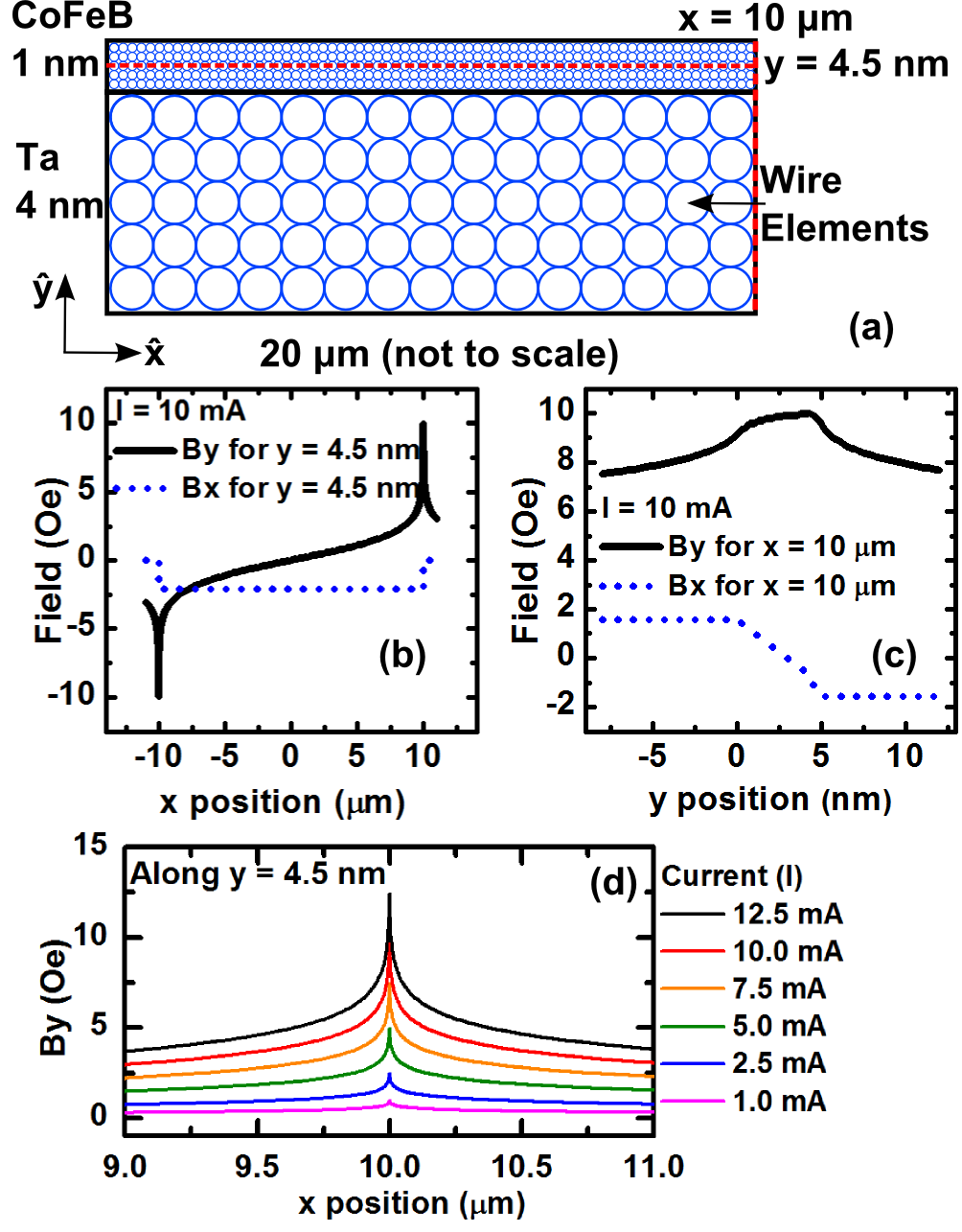
In Fig.5 the direction has again been defined along the width of the Hall bar ( m) while lies perpendicular to the plane. Fig.5.(b) shows and along a line through the center of the CoFeB layer at y nm for mA. The field profile is as expected for a current carrying stripKeatley2008 and is in good agreement with fields calculated in ref.(17). We observe a sharp peak in with height of about Oe close to the edges of the bar. These fields are comparable to the Oe out of plane coercive fields observed for this device in Fig.1. The magnitude of the Oersted field varies little through the thickness of the CoFeB layer as shown at the field peak around (x m), in Fig.5.(c). These results in conjunction with Fig.4 may explain the domain behaviour at the edges of the device. On one edge aids the reversal of domains whilst on the opposite edge it opposes it. This effect may be lessened as and hence are reduced as shown in Fig.5.(d). Even for mA the Oersted field is still about of the coercive field, and so is still likely to influence the switching process.
With recent interest in resolving the contributions of several mechanisms to the switching of similar devices, this result shows that Oersted fields may not always be discounted when interpreting the relative contribution of each switching mechanism, and also that care must be taken when designing devices of this type. A simple method of minimising , so as to explore only the spin-torque contributions to the switching, is therefore to perform a post deposition etch to remove CoFeB at the edges of the Hall bar, leaving only the Ta underlayer. In the majority of recent studies the HM underlayer has been thicker than the FM layer and so carries the majority of current, meaning that perpendicular Oersted fields in the FM would be effectively minimised by this approach. Another approach to studying the spin transfer torque is to apply an in-plane external magnetic field to the structure, so that switching occurs via coherent rotationHao2015 of magnetization rather than by domain nucleation and growth.
IV Summary
Current induced switching in perpendicularly magnetised Ta/CoFeB/MgO layers was studied by simultaneous Kerr microscopy and electrical transport measurements, focusing on currents close to the critical value for switching. For zero applied magnetic field we find the switching to be a stochastic domain wall driven process, the speed of which is strongly dependent upon the value of the applied current. The nucleation of reverse domains appears to begin at one edge of the device, before these domains then grow towards the center of the Hall bar. Modelling the Oersted field through the cross section of the Hall bar reveals that the out of plane component is comparable to the 10 Oe out-of-plane coercive field of the CoFeB, suggesting that the Oersted field may assist the initial domain nucleation on one edge of the Hall bar while opposing reversal on the other edge.
With recent interest in utilising Ta/CoFeB/MgO layers in perpendicular magnetic tunnel junctions this study highlights the need for careful consideration of the Oersted field when analysing potential contributions to the switching process. Minimisation of the Oersted field contribution, to facilitate study of spin-torques, can be achieved by etching the CoFeB layer at the edge of the device, although it may be possible to also utilise these fields to improve switching efficiency in future technologies.
Acknowledgements
The authors wish to thank Tom Loughran, Rob Valkass, Paul Keatley, Wenzhe Chen and Shu-tong Wang for assistance and discussion. This work was supported by the University of Exeter through the award of a scholarship to CJD, and at Brown University by the Nanoelectronics Research Initiative (NRI) through the Institute for Nanoelectronics Discovery and Exploration (INDEX), and by the National Science Foundation through Grant No. DMR-1307056.
References
- [1] Zvonimir Z. Bandic and Randall H. Victora. Advances in Magnetic Data Storage Technologies. Proceedings of the IEEE, 96(11):1749–1753, November 2008.
- [2] Emre Kultursay, Mahmut Kandemir, Anand Sivasubramaniam, and Onur Mutlu. Evaluating STT-RAM as an energy-efficient main memory alternative. In 2013 IEEE International Symposium on Performance Analysis of Systems and Software (ISPASS), pages 256–267. IEEE, April 2013.
- [3] John Carter and Karthick Rajamani. Designing Energy-Efficient Servers and Data Centers. Computer, 43(7):76–78, July 2010.
- [4] Urs Hoelzle and Luiz Andre Barroso. The Datacenter as a Computer: An Introduction to the Design of Warehouse-Scale Machines. May 2009.
- [5] S Ikeda, K Miura, H Yamamoto, K Mizunuma, H D Gan, M Endo, S Kanai, J Hayakawa, F Matsukura, and H Ohno. A perpendicular-anisotropy CoFeB-MgO magnetic tunnel junction. Nature materials, 9(9):721–4, September 2010.
- [6] H. Almasi, D. Reifsnyder Hickey, T. Newhouse-Illige, M. Xu, M. R. Rosales, S. Nahar, J. T. Held, K. A. Mkhoyan, and W. G. Wang. Enhanced tunneling magnetoresistance and perpendicular magnetic anisotropy in Mo/CoFeB/MgO magnetic tunnel junctions. Applied Physics Letters, 106(18):182406, May 2015.
- [7] Xuepeng Qiu, Praveen Deorani, Kulothungasagaran Narayanapillai, Ki-Seung Lee, Kyung-Jin Lee, Hyun-Woo Lee, and Hyunsoo Yang. Angular and temperature dependence of current induced spin-orbit effective fields in Ta/CoFeB/MgO nanowires. Scientific reports, 4:4491, January 2014.
- [8] C. Zhang, M. Yamanouchi, H. Sato, S. Fukami, S. Ikeda, F. Matsukura, and H. Ohno. Magnetization reversal induced by in-plane current in Ta/CoFeB/MgO structures with perpendicular magnetic easy axis. Journal of Applied Physics, 115(17):17C714, May 2014.
- [9] Junyeon Kim, Jaivardhan Sinha, Masamitsu Hayashi, Michihiko Yamanouchi, Shunsuke Fukami, Tetsuhiro Suzuki, Seiji Mitani, and Hideo Ohno. Layer thickness dependence of the current-induced effective field vector in Ta/CoFeB/MgO. Nature materials, 12(3):240–5, March 2013.
- [10] Jacob Torrejon, Felipe Garcia-Sanchez, Tomohiro Taniguchi, Jaivardhan Sinha, Seiji Mitani, Joo-Von Kim, and Masamitsu Hayashi. Current driven asymmetric magnetization switching in perpendicularly magnetized CoFeB/MgO heterostructures. October 2014.
- [11] Xuepeng Qiu, Kulothungasagaran Narayanapillai, Yang Wu, Praveen Deorani, Xinmao Yin, Andrivo Rusydi, Kyung-Jin Lee, Hyun-Woo Lee, and Hyunsoo Yang. A new route to spin-orbit torque engineering via oxygen manipulation. e-print arXiv:1311.3032, November 2013.
- [12] Qiang Hao and Gang Xiao. Giant spin Hall effect and magnetotransport in a Ta/CoFeB/MgO layered structure: A temperature dependence study. Physical Review B, 91(22):224413, June 2015.
- [13] D. C. Worledge, G. Hu, David W. Abraham, J. Z. Sun, P. L. Trouilloud, J. Nowak, S. Brown, M. C. Gaidis, E. J. O’Sullivan, and R. P. Robertazzi. Spin torque switching of perpendicular Ta/CoFeB/MgO-based magnetic tunnel junctions. Applied Physics Letters, 98(2):022501, January 2011.
- [14] Can Onur Avci, Kevin Garello, Corneliu Nistor, Sylvie Godey, Belén Ballesteros, Aitor Mugarza, Alessandro Barla, Manuel Valvidares, Eric Pellegrin, Abhijit Ghosh, Ioan Mihai Miron, Olivier Boulle, Stephane Auffret, Gilles Gaudin, and Pietro Gambardella. Fieldlike and antidamping spin-orbit torques in as-grown and annealed Ta/CoFeB/MgO layers. Physical Review B, 89(21):214419, June 2014.
- [15] Shoji Ikeda, Jun Hayakawa, Young Min Lee, Fumihiro Matsukura, Yuzo Ohno, Takahiro Hanyu, and Hideo Ohno. Magnetic Tunnel Junctions for Spintronic Memories and Beyond. IEEE Transactions on Electron Devices, 54(5):991–1002, May 2007.
- [16] D. Lacour, J. A. Katine, N. Smith, M. J. Carey, and J. R. Childress. Thermal effects on the magnetic-field dependence of spin-transfer-induced magnetization reversal. Applied Physics Letters, 85(20):4681, November 2004.
- [17] Luqiao Liu, O. J. Lee, T. J. Gudmundsen, D. C. Ralph, and R. A. Buhrman. Current-Induced Switching of Perpendicularly Magnetized Magnetic Layers Using Spin Torque from the Spin Hall Effect. Physical Review Letters, 109(9):096602, August 2012.
- [18] Guoqiang Yu, Pramey Upadhyaya, Yabin Fan, Juan G Alzate, Wanjun Jiang, Kin L Wong, So Takei, Scott A Bender, Li-Te Chang, Ying Jiang, Murong Lang, Jianshi Tang, Yong Wang, Yaroslav Tserkovnyak, Pedram Khalili Amiri, and Kang L Wang. Switching of perpendicular magnetization by spin-orbit torques in the absence of external magnetic fields. Nature nanotechnology, 9(7):548–54, July 2014.
- [19] Luqiao Liu, Chi-Feng Pai, Y Li, H W Tseng, D C Ralph, and R A Buhrman. Spin-torque switching with the giant spin Hall effect of tantalum. Science (New York, N.Y.), 336(6081):555–8, May 2012.
- [20] P. S. Keatley, V. V. Kruglyak, A. Neudert, E. A. Galaktionov, R. J. Hicken, J. R. Childress, and J. A. Katine. Time-resolved investigation of magnetization dynamics of arrays of nonellipsoidal nanomagnets with nonuniform ground states. Physical Review B, 78(21):214412, December 2008.