Large-Scale Experimental and Theoretical
Study of Graphene Grain Boundary Structures
Abstract
We have characterized the structure of 176 different single-layer graphene grain boundaries using 1000 experimental HRTEM images using a semi-automated structure processing routine. We introduce a new algorithm for generating grain boundary structures for a class of hexagonal 2D materials and use this algorithm and molecular dynamics to simulate the structure of 79 000 graphene grain boundaries covering 4122 unique orientations distributed over the entire parameter space. The dislocation content and structural properties are extracted from all experimental and simulated boundaries, and various trends are explored. We find excellent agreement between the simulated and experimentally observed grain boundaries. Our analysis demonstrates the power of a statistically significant number of measurements as opposed to a small number of observations in atomic science. All experimental and simulated boundary structures are available online.
pacs:
PACS numbersI Introduction
Single-layer graphene is a promising material for many technological applications, due to its excellent mechanical Lee et al. (2008); Wei et al. (2012); Rasool et al. (2013) and electronic properties Li et al. (2009); Neto et al. (2009). Most graphene deposition methods produce polycrystalline sheets, containing grain boundaries (GBs) Li et al. (2009); Rasool et al. (2010). This polycrystal structure introduces local property deviations at the boundaries that could limit or enable various potential applications. There is also strong scientific interest in graphene GBs due to their one-dimensional nature. Some examples include a bimodal phonon scattering behaviour across graphene GBs Yasaei et al. (2015), anomalous strength characteristics Grantab et al. (2010a); Rasool et al. (2013), strong chemical sensitivity of boundary charge transform Yasaei et al. (2014), a transformation of the GBs from transparency of charge carriers to near-perfect reflection Yazyev and Louie (2010a), amongst others.
A large number of theoretical studies on graphene GB structures have been performed by many researchers Yazyev and Louie (2010a, b); Liu and Yakobson (2010); Malola et al. (2010); Cockayne et al. (2011); Carlsson et al. (2011); Yi et al. (2013); Zhang and Zhao (2013); Tan et al. (2013); Dai et al. (2014); Vancsó et al. (2014); Grantab et al. (2010b); Zhang et al. (2012a); Song et al. (2013); Liu et al. (2012); Hao and Fang (2012); Sha et al. (2014); Zhang et al. (2012b); Kotakoski and Meyer (2012); Van Tuan et al. (2013); Cao and Qu (2013). However the number of corresponding experimental measurements of free-standing graphene GB structure at atomic resolution is much smaller Huang et al. (2011); An et al. (2011); Kim et al. (2011); Kurasch et al. (2012a); Rasool et al. (2013, 2014). These experimental studies have typically considered either a single boundary structure, or a small number of GB structures. Thus, the gap between the number of possible or proposed graphene GB structures and those experimentally observed is very large. This makes testing the various proposed models for graphene GB structure and structure formation very challenging Yazyev and Louie (2010b); Guo et al. (2015).
In this study, we have characterized the structure 176 graphene GB structures from 1067 phase-contrast high resolution transmission electron microscopy (HRTEM) observations of free-standing single-layer graphene samples. We have characterized the atomic structure using a semi-automated processing routine, measuring the local topology and various other physical parameters. We have also used a new algorithm to generate the structure of 79,000 graphene GBs covering the entire orientation parameter space, which were then relaxed using molecular dynamics (MD). We have performed a detailed structural characterization of all experimental and simulated boundaries, extracting structure parameters and dislocation content of all boundaries. The proposed algorithm for generating graphene GB structures is found to be in excellent agreement with the observed structures.
II Methods: Experimental
II.1 Graphene Sample Fabrication and HRTEM Imaging
Graphene samples were grown on polycrystalline copper substrates at 1035∘C by chemical vapor deposition. The substrate was held at 150 mTorr hydrogen for 1.5 hours in a quartz tube furnace, and then 400 mTorr methane was run (5 sccm) over the sample for 15 minutes to grow single-layer graphene. Further details of this method are described in Refs. Li et al. (2009); Rasool et al. (2010, 2013).
All experimental high-resolution transmission electron microscope (HRTEM) images used in this study were recorded on the TEAM 0.5, a monochromated, aberration-corrected FEI Titan-class microscope, operated at 80 kV with a high brightness Schottky field emission gun. Rather than optimizing the imaging conditions, we instead focused on recording images as quickly as possible so as to minimize electron beam damage of the GBs. Often, multiple images of the same boundary were collected sequentially which allowed for both optimization of the imaging conditions and observations of beam-induced modifications of the structure.
II.2 Semi-Automated Experimental GB Analysis
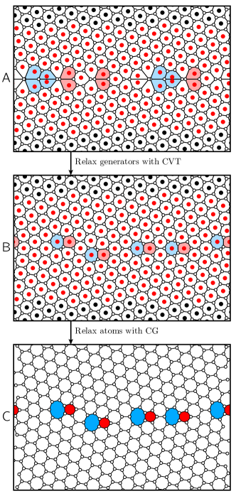
The graphene HRTEM images have a low signal-to-noise ratio due to the low scattering efficiency of single carbon atoms. In order to measure the boundary structure for hundreds of images, we have developed a processing routine with as few user inputs as possible. This routine is shown schematically in Fig. 1. First, a linear background is fitted and removed from the image to minimize the intensity falloff caused by the monochromatic aperture. Next, a nonlinear filter is applied to remove noise (rank filter of local intensity values within a 0.6Å radius, 25 darkest value selected Soille (2002)), shown in Fig. 1B. Peak detection is used to find local minima, and the user inputs the boundary extent, the three locations labeled in Fig. 1C. A subset of the detected peaks given by this user-selected region-of-interest is used to automatically characterize the boundary structure.
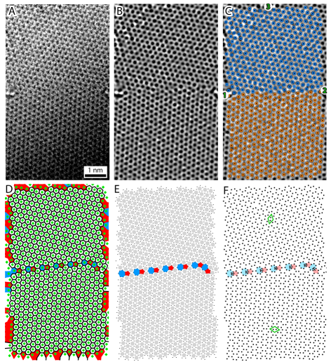
The first step of the boundary characterization is a Voronoi tessellation of the detected local minima, shown in Fig. 1D. The Voronoi cell vertices represent atomic positions. The number of carbon atoms in each ring is given by the number of sides of each cell. Next, the boundary cells are removed and the tessellation is recomputed using a weighted Voronoi algorithm Aurenhammer and Edelsbrunner (1984), with the weights set to keep the mean bond length constant for all cells, shown in Fig. 1E. The final atomic coordinates are plotted in Fig. 1F, with a final optimization performed to enforce a minimum distance constraint of 1.2 Å on all atomic coordinates, to ensure a physically realistic result. The boundary can be traced by connecting all pentagon and heptagon rings, and a best-fit lattice is calculated for the two grains on each side. The dislocations are located by searching for a minimal description of all pentagon-heptagon pairs.
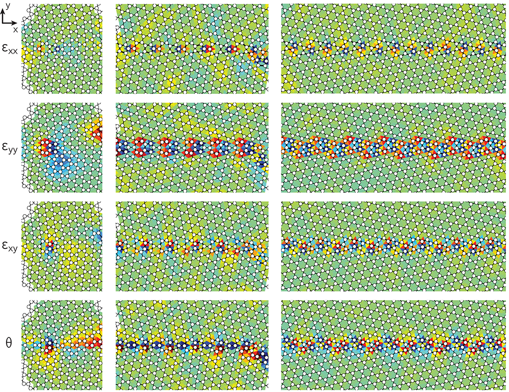
Additionally, the strain of the experimental boundaries was estimated using a geometric method similar to that given in Ref. Mott et al. (1992). Each atom is placed at the center of a triangle defined by its 3 nearest-neighbors, calculated from a Delaunay triangulation of the set of atoms. These triangles are referenced to the appropriate triangle (2 atomic sites per unit cell) formed by the lattice vectors of the best-fit lattices of the two grains. The linear transformation matrix for each triangle is used to calculate local strains (infinitesimal strain is assumed for convenience). Rather than parse the strain into atomic coordinates as in Ref. Mott et al. (1992), we instead calculate the root-mean-square values of the local strains and the local rotation, since we are interested in the “average” distortion of each of the boundaries. Three examples of these strain measurements are given in Fig. 2.
III Methods: Numerical
III.1 Space of Graphene GBs
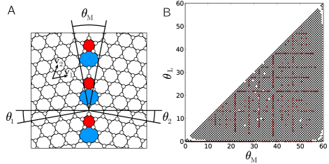
Bulk three-dimensional materials require 5 angles to characterize the macroscopic degrees of freedom of a general GB, while two-dimensional materials require only 2 angles. Thus the parameter space for 2D GBs is far smaller than that of 3D grain boundaries. As shown in Fig. 3 A these two angles are the misorientation angle , defined as the angle between the unit cell vectors of each grain, and the boundary line direction , defined as the angle between the boundary vector and the symmetric tilt boundary vector for a given . Due to the symmetries of the graphene lattice we get and . A third parameter, namely the relatively sliding of the two grains along the GB boundary is also needed for a complete description of the boundary. In our simulations we choose the relative sliding that gives the lowest GB energy, thus effectively eliminating this degree of freedom.
In order to minimize the boundary effects, we simulate GB structures that are periodic along the GB direction. This requirement places strong restrictions on the GB configurations that we can simulate. Consider simulation of the GB corresponding to a point , or equivalently , in the parameter space. The lattice vectors for graphene are , , where is the carbon-carbon bond length, and are unit vectors parallel and perpendicular to the zigzag axis of the graphene sheet, respectively. Thus for given the corresponding grains have periodic repeat distances of () along the GB direction, where are integers such that Saito et al. (1998). For an arbitrary there may exist no suitable integers , or even if such integers exist, can be prohibitively large for MD simulation. Further, in order to simulate a GB, and should either be commensurate, i.e., where are positive integers, in which case the net GB length is given by , or they should be approximately commensurate, i.e., , in which case the simulated GB length is , and each grain has a strain of magnitude . In case of approximately commensurate boundaries, we require that the rational approximation is chosen such that the resulting strain magnitude is less than , so that the resulting elastic distortion is minimal. Due to numerical considerations, we simulated GBs with a maximum length of 2000 Å. If for a given the GB length is greater than 2000 Å, we try to find a nearby GB such that the resulting grain angles are within 0.01∘ of the desired values. Finally, in order to choose the relative sliding between the two grains that leads to minimum GB energy, we search in steps of 1 Å over the entire range Coffman and Sethna (2008), given by
| (1) |
assuming . We simulate all perfectly commensurate GBs with length less than 2000 Å , and grid the space in steps of , resulting in a ‘diagonal gridding’ of the space in steps of . However, for certain configurations near no approximately commensurate boundaries with length less than 2000 Å could be found, and thus no boundaries were simulated at these grid points. Fig. 3B shows for all GBs configurations that we simulated (4122 total). Each point in that figure represents several simulations due to the sampling of the relative sliding . In all we have simulated over 79,000 GB structures for this study.
III.2 Numerical GB Structure Generation Algorithm
Experimental observations of well annealed graphene GBs in the present study, as well as by several previous authors, Huang et al. (2011); An et al. (2011); Kim et al. (2011); Kurasch et al. (2012b, a); Lee et al. (2013); Rasool et al. (2013, 2014) suggests that the orientation change between adjacent grains meeting at a GB is mediated largely by pairs of rings of 5 and 7 carbon atoms. These pentagon-heptagon pairs, also called the 5-7 pairs, are the dislocation cores with the shortest Burgers vectors in graphene, and have a low formation energy Yazyev and Louie (2010b). Thus, it is reasonable to expect that graphene GBs simulated on a computer have atomic structures where the orientation change between the grains is mediated mostly by the experimentally observed pentagon-heptagon pairs. However, it is difficult to meet this requirement in practice. While a few simple GBs composed solely of pentagon-heptagon pairs have been simulated successfully Grantab et al. (2010b); Zhang et al. (2012a); Song et al. (2013); Liu et al. (2012); Hao and Fang (2012), deviations from this motif are evident in the GB and polycrystals used in several recent studies Sha et al. (2014); Zhang et al. (2012b); Kotakoski and Meyer (2012); Van Tuan et al. (2013); Cao and Qu (2013). The reason for this limitation is that so far no computationally efficient method has been proposed to generate well-annealed graphene GBs on a computer. Methods based on grand canonical Monte Carlo simulations, while theoretically sound and simple to implement, take inordinately large amount of computer time in practice. The common method of simply “annealing” a grain boundary by running molecular dynamics at an elevated temperature is also not effective since the typical thermal barriers that need to be overcome for suitable reconstruction are high, and thus the desired annealing does not occur in the limited simulation time. For simple GBs these limitations can be overcome by the inclination-disclination based geometric method Yazyev and Louie (2010b). This geometrical approach is well suited for the study of simple GBs, but becomes unwieldy for tailoring more complex GBs or polycrystals with several different GBs and junctions.
To create physically realistic graphene GBs with dislocation density as close as possible to the geometrically required density, we propose an algorithm based on the centroidal Voronoi tessellation (CVT). Before describing the algorithm in detail, we give an intuitive explanation. A triangular lattice can be associated to the graphene lattice via a Voronoi construction (also known as the Dirichlet or Weigner-Seitz construction, or the dual construction), and vice-versa. For example, in Fig. 4B the graphene lattice (open black circles) forms the vertices of the Voronoi cells of the triangular lattice (dark red circles), and vice-versa. As discussed earlier, it is difficult to anneal a graphene GB by using classical Monte Carlo methods. If however, one could find a method to anneal the associated triangular lattice, then the graphene GB could be easily recovered from the well annealed triangular lattice by applying the Voronoi construction. Notice that annealing the triangular lattice by using Monte Carlo or MD will be almost as difficult as annealing the original graphene lattice with similar techniques. The interesting part of our algorithm uses the CVT to efficiently anneal the triangular lattice, and a well annealed graphene GB is recovered from it via a Voronoi construction.
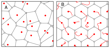
We give a brief introduction to CVTs; details can be found in any number of references including Refs. Du et al. (1999); Liu et al. (2009). Let , be a set of points in a compact connected region . (the generalization to is analogous). The points will be called the generators of the Voronoi tessellation. The Voronoi region corresponding to the generator is defined as the set of all points that are closer (or equidistant) to it than to any other generator, i.e., where is the usual Euclidean norm. We denote the set of the vertices of the Voronoi regions by . Fig. 4A shows an example of a 2D periodic Voronoi tessellation with generators. Clearly, the centroid of the region is in general distinct from its generator . If we demand that the generators be arranged so that the centroids of the resulting regions coincide with their generators, then we get a CVT. A CVT can also be described in terms of a variational problem Liu et al. (2009). It has been noted that the generators of a CVT are local or global minimizers of the following energy function
| (2) |
Fig. 4B shows an example of a 2D-periodic centroidal Voronoi tessellation with generators. Note that the vertices of the Voronoi regions form a graphene-like hexagonal lattice, while the generators form a triangular lattice. In fact, it is a general property of CVTs that they tend to generate a tessellation with regular hexagonal regions of equal size Du et al. (1999); Liu et al. (2009). The tessellation shown in Fig. 4B is obtained by starting from the configuration of generators shown in 4A and moving them according to Lloyd’s algorithm so as to minimize the energy function Du et al. (1999); Liu et al. (2009). The path traced by each generator under the action of this algorithm is shown by the red lines in Fig. 4B. We choose the aspect ratio of the domain such that it is possible to tile it with 16 regular hexagons. The tessellation is 2D-periodic because we implement 2D-periodic boundary conditions in our metric . A perfect tessellation with equal regular hexagons does not always exist, and neither does Lloyd’s algorithm converge to it from every possible initial condition even if it exists. For example, if we take generators, then a perfect tessellation is impossible. In such cases, CVTs try to minimize the deviation from perfect hexagons, and on most occasions find a tessellation containing suitable pentagons-heptagons defects.
The CVT based algorithm for generating graphene GBs is as follows. Given a GB the goal is to decide the positions of carbon atoms so that on each side of the GB the graphene sheet has the desired orientation, while the GB is comprised mostly of pentagon-heptagon dislocations (or undefected hexagons). To achieve this goal, the algorithm first generates a triangular lattice dual to the graphene lattice with suitable orientation on each side of the GB. Fig. 5A shows an example of this construction. At this point, the Voronoi regions (with the triangular lattice points as generators) contain suitably aligned hexagons away from the GB, but near the boundary the structure is not composed of well-aligned pentagon-heptagon pairs, as shown in the figure. The generators (triangular lattice points) close to the grain boundaries are then relaxed by using Lloyd’s algorithm to obtain a CVT while keeping the points that are sufficiently far away from the boundaries fixed. The fixed points are shown by black circles, while the points that are relaxed by Lloyd’s algorithm are shown in red circles in Fig. 5. After the relaxation has converged, we obtain a 2D-periodic Voronoi tessellation for the entire lattice, and obtain a graphene GB by placing a carbon atom at each vertex of the tessellation. Fig. 5B shows the graphene GB corresponding to the grain structure of Fig. 5A obtained after this relaxation. We see that the grain interiors are defect free and have the desired orientations, while the GB is mediated by well-aligned pentagon-heptagon pairs. Finally, the atomic positions can be fine tuned by using the congugate gradients method and an atomistic potential; we use the AIREBO potential in this study Brenner et al. (2002). The graphene GB obtained after this fine tuning is shown in Fig. 5C. This final step only leads to small changes in the atomic positions, and does not entail any larger topological rearrangements of rings and defects. The numerical implementation is efficient, and we are able to obtain a well annealed GBs that are hundreds of nanometers long in a matter of minutes on a laptop.
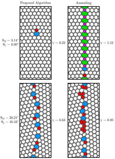
We have compared the GB structures generated with the proposed algorithm with the other widely used methods of generating GBs. One popular technique is to paste together two half crystals of the required orientations and anneal the system by running molecular dynamics at an elevated temperature Sha et al. (2014). We use this technique, where we heat the GB from 10 K to 3000 K, and then cool it back to 10 K in a span on 100 ps. The final configuration is then relaxed by using the conjugate gradient method. During this entire process a 10 Å strip of atoms on the left and right edges of the system are constrained to their ideal crystalline positions. The net width of the system excluding the constrained atoms is 50 Å. Fig. 6 shows the comparison of two GB structures obtained with this method to those obtained by the CVT based method proposed here. The GBs have identical number of atoms, and identical atomic positions away from the boundary. We evaluate the GB energy per-unit length, defined as , where is the net potential energy of the unconstrained atoms, and eV is the ground state energy per atom in graphene according to the AIREBO potential. It is evident that for the examples shown in Fig. 6 proposed method outperforms the method of annealing as it generates GBs with lower energies. We have tested several hundred GBs, and the proposed method always performs better than the method of annealing.
To understand why this boundary generation algorithm outperforms the traditional method of annealing or grand canonical Monte Carlo or simple energy minimization, we note that the energy landscape of the CVT Hamiltonian is in some sense more favorable than that of the conventional atomistic potential based Hamiltonian. While just like the atomistic potentials, the CVT Hamiltonian can have several local minima, it seems that unlike the atomistic potentials, all its local minima represent low energy configurations of the polycrystalline graphene sheet. In a perfect tessellation, each generator contributes two vertices, thus removing or adding a generator is analogous to creating a vacancy pair or an adatom pair. This is a very desirable property, since it ensures that isolated vacancies or adatoms never appear, as these are high energy defects Banhart et al. (2011). All the vacancy pair and adatom pair defects generated by removing and adding generators are shown in the supplemental material and correspond to low energy configurations of vacancy and adatom pairs. Thus, the algorithm is able to produce realistic grain boundaries as well as point defects.
The CVT Hamiltonian is oblivious of all the nuanced and complicated interactions between carbon atoms, as it takes a geometric view of the problem. This is a strength and a weakness of this approach. Its strength is clearly demonstrated in the high quality structures that it can generate at modest numerical cost. Its weakness would be that it is hard, if not impossible, to modify this approach to include, say, the effect of chemical interactions with hydrogen (or another element) on structure of the GB. However, since the structure and properties of pure graphene GBs and similar two-dimensional materials are of such wide interest, we think that the proposed method has broad merit. Finally, it should be noted that the primary role of the CVT algorithm is to relax the triangular lattice. As mentioned before, it is not feasible to simply use a LJ potential (or another pair potential, or hard spheres etc.) to relax this triangular lattice and simplify this algorithm. Thus, the unique properties of the CVT truly offer an advantage over pair potentials and Monte Carlo based methods in this case.
IV Results and Discussion
The full library of our measured experimental GB structures is available at the experimental structures archive. The full library of our simulated GB structures is available at the computed structures archive.
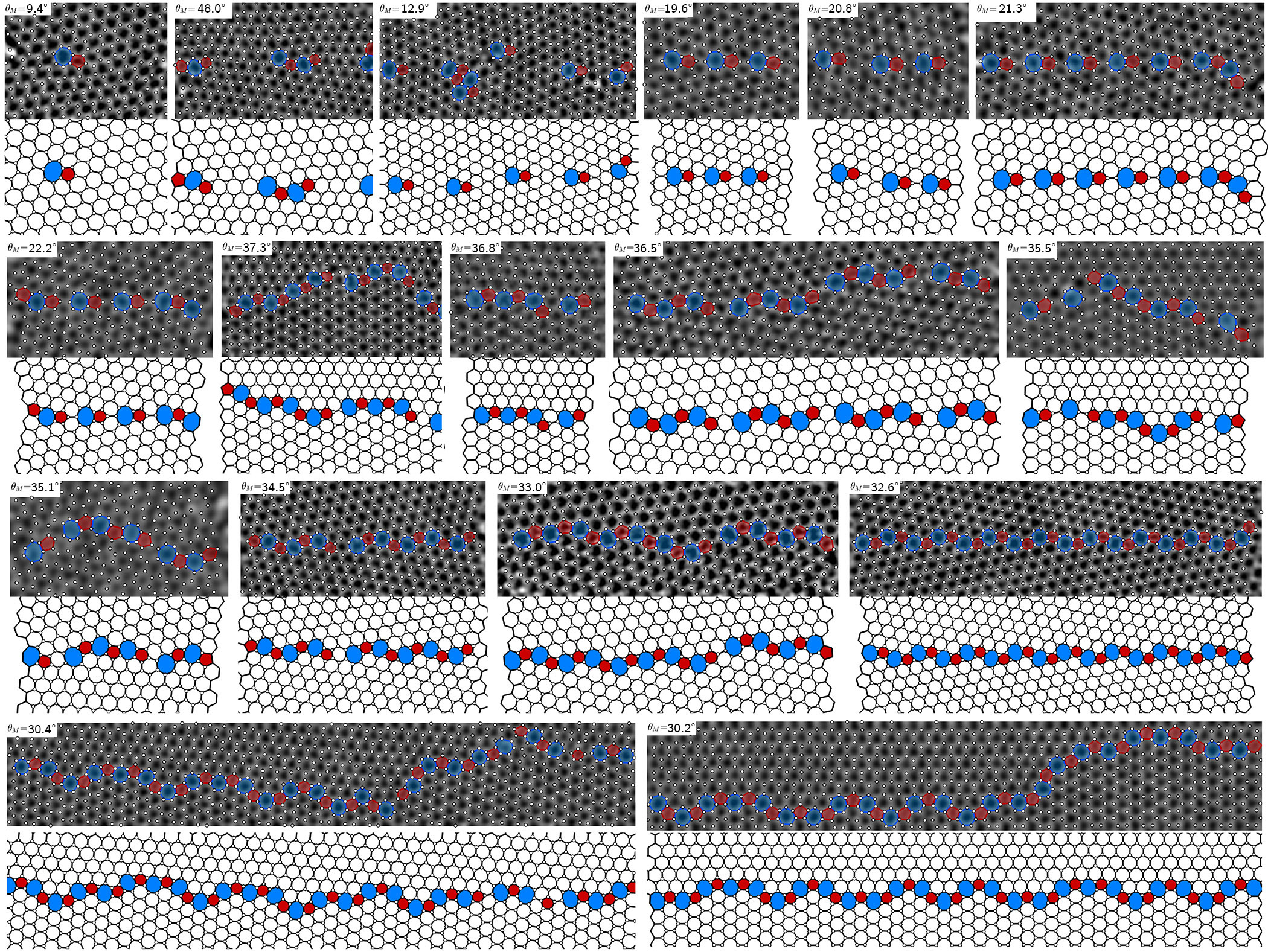
Fig. 7 shows 17 examples of experimentally measured GB structures, ranging from low to high boundary disorientations . These misorientations are calculated from the best-fit lattices of the two grains, with an estimated error of approximately 0.5∘. The low angle boundaries are composed of isolated pentagon-heptagon pairs, while the higher angle boundaries are composed of connected pentagon-heptagon pairs. Each experimental boundary is paired with a matching example taken from the generated boundary library, with either an identical or very similar structure. The close agreement demonstrates the efficacy of our boundary generation algorithm.
IV.1 Simulated Grain Boundary Structures
A small subset of the numerically simulated GB structures are plotted in Fig. 8A. The 5-member pentagon rings are colored in red, while the 7-member heptagon rings are colored in blue. Each pentagon-heptagon pair sharing a C-C bond represents a (1,0) dislocation core with the smallest possible Burgers vector, while a pentagon-heptagon pair connected by a C-C represents a (1,1) dislocation core with the next-smallest Burgers vector Yazyev and Louie (2010b). Separating the pentagon and hepagon by a single 6-member hexagon ring leads to a (2,0) dislocation with a Burgers vector with twice the magnitude of the (1,0) dislocations. Fig. 8B shows the atomic structure of these dislocations graphically.
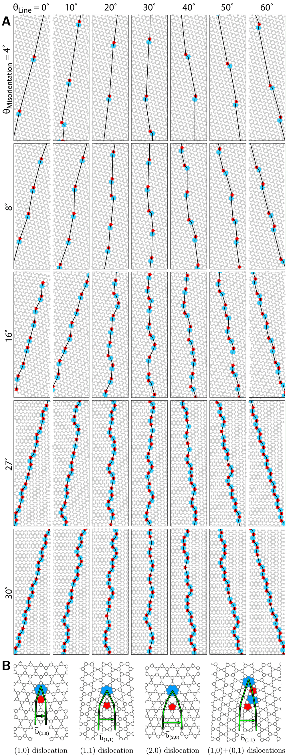
Fig. 8B also shows another commonly observed dislocation structure; pairs of (1,0) and (0,1) dislocations. These dislocation pairs have the same Burgers circuit as the (1,1) dislocation. These dislocation pairs are typically much lower energy than (1,1) dislocations and are commonly observed in the range , and are especially prevalent in for misorientation angles Yazyev and Louie (2010b).
IV.2 Structural Properties of Simulated Boundaries
We have used automated analysis routines to extract the dislocation content and structural properties from all of the lowest-energy simulated boundaries for each value of and . Figs. 9A-F plot the dislocation content of the simulated boundaries. The most common boundary structures by a large margin (over 98%) are the (1,0) and paired (1,0)+(0,1) dislocations. Figs. 9B and C show that the pairing arrangement is much more common for boundaries with , although many pairs are also present for the most asymmetric boundaries (high ).
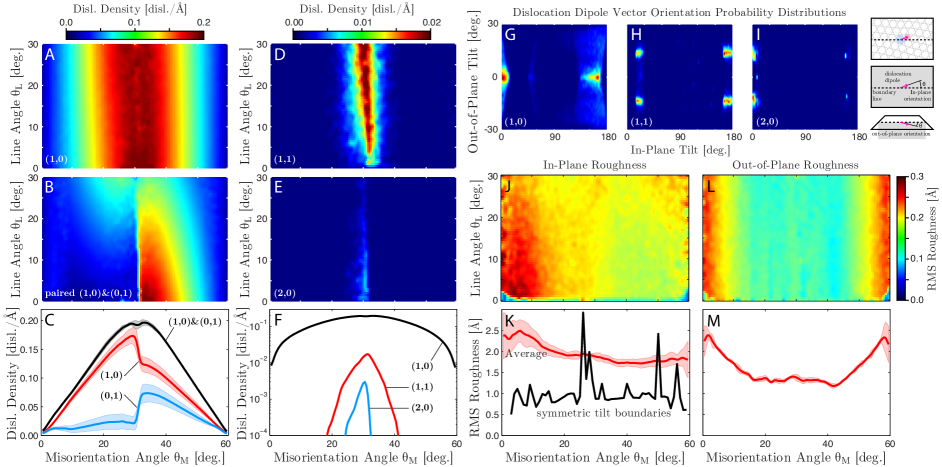
Figs. 9D and E plot the density of (1,1) and (2,0) dislocations, both of which are almost entirely present only in boundaries with high disorientations, . The peak density of (1,1) and (2,0) dislocations is approximately 10 and 60 times lower than the (1,0) dislocation density respectively, shown in Fig. 9F. (1,1) dislocations are slightly more prevalent at higher values, while (2,0) dislocations have higher density at lower values.
We have also analyzed the three-dimensional orientation densities of the dislocation dipole vectors, defined as the vector from the center of each heptagon to its associated pentagon. The 2D probability distributions of all dislocations (equally weighted for each calculated boundary) over in-plane and out-of-plane dipole tilt vectors are plotted in Figs. 9G, H and I for (1,0), (1,1) and (2,0) dislocations respectively. The (1,0) dislocations tend to align along the boundary line, with two large clusters visible in Fig. 9G; the left cluster is formed from the lower boundaries while the cluster to the right contains more high boundaries. These right-side (1,0)-type dislocations tend to be slightly tilted away from the boundary line vector and are often paired with a (0,1)-type dislocation, giving a longer tail towards lower values in this cluster. A third, very dim cluster is visible at approximately in-plane tilt values. All three of these clusters are centered on out-of-plane tilt, with the distributions decreasing quickly at higher and lower out-of-plane tilt values. All three clusters have a range of approximately for the out-of-plane tilt. By contrast, Fig. 9H shows that the (1,1)-type dislocations have a strongly bimodal probability distribution for both in-plane and out-of-plane tilts, occur primarily at in-plane tilts of and and out-of-plane tilts of . The (2,0)-type dislocation orientations are plotted in Fig. 9I, showing maxima at an in-plane tilt of and out-of-plane tilts of .
The roughness of all simulated boundaries was estimated by connecting all boundary pentagons and heptagons sequentially, and measuring the root-mean-square (RMS) displacement of this distorted boundary line, both in-plane and out-of-plane of the graphene sheet. The in-plane RMS roughness is plotted in Fig. 9J as a function of the boundary angles. The mean and standard deviation of the roughness averaged over all values is plotted in Fig. 9K. The in-plane boundary roughness is largest at low values, decreasing from approximately to with increasing . The in-plane roughness of the symmetric tilt boundaries are also plotted in Fig. 9. Most symmetric tilt boundaries have lower roughness than the average of all boundaries, approximately 1Å, except for a small number of boundaries spiking at RMS roughness values of 3Å. The out-of-plane RMS roughness of all boundaries is plotted in Figs. 9L and M. These roughness values are much more uniform that the in-plane roughness; between and the roughness decreases from to 1.3Å. From and the roughness is almost constant at 1.3Å. Finally, between and the roughness increases from to 2.4Å. The symmetric boundaries do not show any deviation in out-of-plane roughness compared to the average values. The boundaries with larger disorientations have higher dislocation densities; this allows their overlapping strain fields to more easily cancel out and therefore lead to lower out-of-plane roughness.
IV.3 Structural Properties of Experimental Boundaries
The physical properties and structure of the experimental boundaries were also characterized with automated routines. These results are shown in Fig. 10. Some examples of symmetric tilt boundaries with structures similar to those plotted in Fig. 7 are depicted in Fig. 10A. The experimental results plotted in the rest of Fig. 10 are 160 boundaries estimated to be unique structures. We took this step to try to minimize double counting of boundary structure datapoints. We observe that most of the boundary structures we measured fall at high disorientation angles, i.e. boundaries close to . This phenomenon is due to topological effects; low angle boundaries have rougher surfaces and long range out-of-plane distortions Liu and Yakobson (2010). This topology in turn attracts carbon contamination due to surface charging, which obscures the boundary. The imaging process is therefore biased towards flatter boundaries, i.e. those closer to .
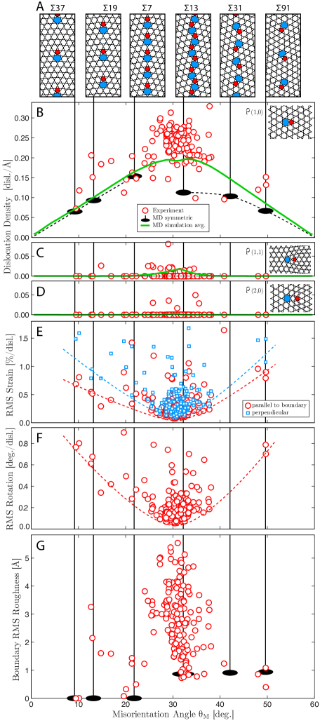
Figs. 10B, C and D shows the measured densities as a function of misorientation angle for (1,0), (1,1), and (2,0) dislocations respectively. These figures also show the (1,0) dislocation densities of the 6 symmetric boundaries plotted in Fig. 10, and the dislocation densities of all three types predicted from the simulated boundary relaxations in Fig. 9F. The experiments are in good agreement with both of these sets of predictions. All of the 6 symmetric boundaries shown in Fig. 10A have a nearby experimental example. However at misorientation angles in the range , in the highest density region of the experimental boundaries, the average predictions of the relaxed and constructed boundaries are much closer to the majority of experimental dislocation densities. The simulated boundaries also predict a small concentration of (1,1)- and (2,0)-type dislocations in the range , both of which are observed in the experimental measurements shown in Figs. 10C and D. The average dislocation concentrations of the experiments are very close to the simulations, with the exception of a single (1,1) dislocation observed in an experiment at .
Because the experimental boundaries are measured as a 2D projection, the out-of-plane distortions cannot be directly measured. However, these distortions are typically accompanied by large deviations in the local projected atomic positions. We have therefore measured the average strains and local rotations of all boundaries, plotting in Figs. 10E and F, normalized by the dislocation density. All of the average strain metrics have approximately the same trend; they decrease as the misorientation increases, and then the strain increases past . This is qualitatively in agreement with the predictions of out-of-plane roughness trends shown in Fig. 9M. The RMS strain perpendicular to the grain boundaries is large than the parallel strain for virtually all boundaries, shown in Fig. 10E. This is because dislocation dipoles are typically aligned along the grain boundaries, which allows the adjacent dislocation strain fields to partially cancel out.
The boundary RMS roughness for all experimental boundaries is plotted in Fig. 10F. Five of the six symmetric boundaries plotted in Fig. 10A predict boundary roughness values that are very close matches to the experiments. The largest concentration of boundaries near the center of the plot reach a minimum roughness at a misorientation value closer to the value of . The entire cluster of values has an average in-plane RMS roughness of approximately 2.5Å, in good agreement with the synthetic boundary prediction of 2Ågiven in Fig. 9K.
IV.4 Matching Experimental and Simulated Structures
The vast majority of experimentally measured GBs and all of the numerically simulated GBs in this study can be constructed by mixing the dislocations structures shown in Fig. 8B. Symmetric boundaries with contain aligned (1,0) dislocations, while non-symmetric boundaries and boundaries with are typically composed of a mixture of (1,0) and (0,1) dislocations Yazyev and Louie (2010b). The ratio of the number of the two most common orientations for (1,0) dislocations could be used to estimate the boundary line angle , but for many of the experimental images the boundary length is too short (not enough observed dislocations) for an accurate measurement of the line angle.
As predicted, the low angle boundaries consist of isolated (1,0) dislocations. At low misorientation angles, all of the (1,0) dislocations have the same orientation, while at high misorientation angles (e.g. ) the structure consists of (1,0) and (0,1) dislocation pairs. Three of the plotted examples in Fig. 7, , , and , have structures very similar to the special boundary Heckl and Binnig (1992); Simonis et al. (2002); Yazyev and Louie (2010b). The boundary is a nearly perfect example of the special boundary Yazyev and Louie (2010b).
The high angle boundaries in Fig. 7 are formed from continuous or near-continuous dislocation groups with alternating 5- and 7-member rings. This structure is expected, since a more equal local density of pentagons and heptagons leads to a lower net disclination content and thus less 3D topological variation, and more stable structures Liu and Yakobson (2010). The longest high angle boundaries in Fig. 7 () show an interesting deviation from the flat boundary structures; they form serpentine structures similar to some literature predictions and observations Huang et al. (2011); Tison et al. (2014); Vancsó et al. (2014) as well as our previous experiments Rasool et al. (2013, 2014). Both of these boundaries exhibit two relatively sharp deviations from a flat boundary line, where the arm-chair and zig-zag graphene edges of the two sides exchange identities. These structures likely originate from capillary fluctuations during the initial growth, but form (relatively) well-defined faceted edges rather than a rougher boundary.
Overall, the boundary generation algorithm therefore accurately predicts structural properties of the experimental boundaries. The primary disagreement is the slightly higher boundary roughness and dislocation density of the high angle boundaries near . The source of this minor disagreement lies in the faceting exhibited by the experimental boundaries, such the bottom two experimental structure plots in Fig.7. Since the simulated boundaries were constrained to follow a single line angle (flat boundaries), they could not fully capture this effect. However, our CVT algorithm could easily be used to simulate such boundaries. This example shows how large-scale experiment and simulations couple together, where the different areas of agreement or disagreement can be used to improve structure models.
V Conclusion
In summary, we have used semi-automated processing routines to characterize the structure of a very large number of experimentally measured single-layer graphene grain boundaries and described their local atomic structure as a function of misorientation angle. We have also introduced a new algorithm for generating realistic graphene grain boundaries that produces structures in excellent agreement with the experimental boundary structures. We have used a combination of our algorithm and molecular dynamics to generate and relax graphene grain boundary structures covering the entire orientation parameter space for single-later graphene boundaries. The structure and physical properties of these simulated boundaries were analyzed as a function of misorientation and boundary line angles. A detailed comparison of the experimental and simulated boundaries demonstrates that our structural models have high predictive power for the experimental structures. In a forthcoming study, we will analyze the energetics of both experimental and simulated grain boundaries. Finally. all experimental and simulated structures are made available on the internet. We hope that this paradigm of computer-assisted analysis of a statistically relevant number of structures and availability of all measured data becomes standard for the study of atomic-resolution structures.
VI Acknowledgements
Work at the Molecular Foundry was supported by the Office of Science, Office of Basic Energy Sciences, of the U.S. Department of Energy under Contract No. DE-AC02-05CH11231. CO thanks Matt Bowers, Ulrich Dahmen and Josh Kacher for useful discussions. AS acknowledges financial support from the Miller Institute for Basic Research in Science, at University of California, Berkeley, in the form of a Miller Research Fellowship, and thanks Robert O. Ritchie for hosting him at the Lawrence Berkeley National Laboratory.
References
- Lee et al. (2008) C. Lee, X. Wei, J. W. Kysar, and J. Hone, Science 321, 385 (2008).
- Wei et al. (2012) Y. Wei, J. Wu, H. Yin, X. Shi, R. Yang, and M. Dresselhaus, Nature materials 11, 759 (2012).
- Rasool et al. (2013) H. I. Rasool, C. Ophus, W. S. Klug, A. Zettl, and J. K. Gimzewski, Nature Communications 4 (2013).
- Li et al. (2009) X. Li, W. Cai, J. An, S. Kim, J. Nah, D. Yang, R. Piner, A. Velamakanni, I. Jung, E. Tutuc, et al., Science 324, 1312 (2009).
- Neto et al. (2009) A. C. Neto, F. Guinea, N. Peres, K. S. Novoselov, and A. K. Geim, Reviews of Modern Physics 81, 109 (2009).
- Rasool et al. (2010) H. I. Rasool, E. B. Song, M. J. Allen, J. K. Wassei, R. B. Kaner, K. L. Wang, B. H. Weiller, and J. K. Gimzewski, Nanoletters 11, 251 (2010).
- Yasaei et al. (2015) P. Yasaei, A. Fathizadeh, R. Hantehzadeh, A. K. Majee, A. El-Ghandour, D. Estrada, C. Foster, Z. Aksamija, F. Khalili-Araghi, and A. Salehi-Khojin, Nanoletters (2015).
- Grantab et al. (2010a) R. Grantab, V. B. Shenoy, and R. S. Ruoff, Science 330, 946 (2010a).
- Yasaei et al. (2014) P. Yasaei, B. Kumar, R. Hantehzadeh, M. Kayyalha, A. Baskin, N. Repnin, C. Wang, R. F. Klie, Y. P. Chen, P. Král, et al., Nature communications 5 (2014).
- Yazyev and Louie (2010a) O. V. Yazyev and S. G. Louie, Nature materials 9, 806 (2010a).
- Yazyev and Louie (2010b) O. V. Yazyev and S. G. Louie, Physical Review B 81, 195420 (2010b).
- Liu and Yakobson (2010) Y. Liu and B. I. Yakobson, Nanoletters 10, 2178 (2010).
- Malola et al. (2010) S. Malola, H. Häkkinen, and P. Koskinen, Physical Review B 81, 165447 (2010).
- Cockayne et al. (2011) E. Cockayne, G. M. Rutter, N. P. Guisinger, J. N. Crain, P. N. First, and J. A. Stroscio, Physical Review B 83, 195425 (2011).
- Carlsson et al. (2011) J. M. Carlsson, L. M. Ghiringhelli, and A. Fasolino, Physical Review B 84, 165423 (2011).
- Yi et al. (2013) L. Yi, Z. Yin, Y. Zhang, and T. Chang, Carbon 51, 373 (2013).
- Zhang and Zhao (2013) J. Zhang and J. Zhao, Carbon 55, 151 (2013).
- Tan et al. (2013) S.-H. Tan, L.-M. Tang, Z.-X. Xie, C.-N. Pan, and K.-Q. Chen, Carbon 65, 181 (2013).
- Dai et al. (2014) Q. Dai, Y. Zhu, and Q. Jiang, Physical Chemistry Chemical Physics 16, 10607 (2014).
- Vancsó et al. (2014) P. Vancsó, G. I. Márk, P. Lambin, A. Mayer, C. Hwang, and L. P. Biró, Applied Surface Science 291, 58 (2014).
- Grantab et al. (2010b) R. Grantab, V. B. Shenoy, and R. S. Ruoff, Science 330, 946 (2010b).
- Zhang et al. (2012a) J. Zhang, J. Zhao, and J. Lu, ACS Nano 6, 2704 (2012a).
- Song et al. (2013) Z. Song, V. I. Artyukhov, B. I. Yakobson, and Z. Xu, Nano Letters 13, 1829 (2013).
- Liu et al. (2012) T.-H. Liu, C.-W. Pao, and C.-C. Chang, Carbon 50, 3465 (2012).
- Hao and Fang (2012) F. Hao and D. Fang, Physics Letters A 376, 1942 (2012).
- Sha et al. (2014) Z. D. Sha, Q. Wan, Q. X. Pei, S. S. Quek, Z. S. Liu, Y. W. Zhang, and V. B. Shenoy, Scientific reports 4 (2014).
- Zhang et al. (2012b) T. Zhang, X. Li, S. Kadkhodaei, and H. Gao, Nano Letters 12, 4605 (2012b).
- Kotakoski and Meyer (2012) J. Kotakoski and J. C. Meyer, Phys. Rev. B 85, 195447 (2012).
- Van Tuan et al. (2013) D. Van Tuan, J. Kotakoski, T. Louvet, F. Ortmann, J. C. Meyer, and S. Roche, Nano Letters 13, 1730 (2013).
- Cao and Qu (2013) A. Cao and J. Qu, Applied Physics Letters 102 (2013).
- Huang et al. (2011) P. Y. Huang, C. S. Ruiz-Vargas, A. M. van der Zande, W. S. Whitney, M. P. Levendorf, J. W. Kevek, S. Garg, J. S. Alden, C. J. Hustedt, Y. Zhu, et al., Nature 469, 389 (2011).
- An et al. (2011) J. An, E. Voelkl, J. W. Suk, X. Li, C. W. Magnuson, L. Fu, P. Tiemeijer, M. Bischoff, B. Freitag, E. Popova, et al., ACS nano 5, 2433 (2011).
- Kim et al. (2011) K. Kim, Z. Lee, W. Regan, C. Kisielowski, M. Crommie, and A. Zettl, ACS nano 5, 2142 (2011).
- Kurasch et al. (2012a) S. Kurasch, J. Kotakoski, O. Lehtinen, V. Skákalová, J. Smet, C. E. Krill III, A. V. Krasheninnikov, and U. Kaiser, Nanoletters 12, 3168 (2012a).
- Rasool et al. (2014) H. I. Rasool, C. Ophus, Z. Zhang, M. F. Crommie, B. I. Yakobson, and A. Zettl, Nanoletters 14, 7057 (2014).
- Guo et al. (2015) W. Guo, B. Wu, Y. Li, L. Wang, J. Chen, B. Chen, Z. Zhang, L. Peng, S. Wang, and Y. Liu, ACS nano (2015).
- Soille (2002) P. Soille, Pattern recognition 35, 527 (2002).
- Aurenhammer and Edelsbrunner (1984) F. Aurenhammer and H. Edelsbrunner, Pattern Recognition 17, 251 (1984).
- Mott et al. (1992) P. H. Mott, A. S. Argon, and U. W. Suter, Journal of Computational Physics 101, 140 (1992).
- Saito et al. (1998) R. Saito, G. Dresselhaus, M. S. Dresselhaus, et al., Physical properties of carbon nanotubes, Vol. 35 (World Scientific, 1998).
- Coffman and Sethna (2008) V. R. Coffman and J. P. Sethna, Physical review B 77, 144111 (2008).
- Kurasch et al. (2012b) S. Kurasch, J. Kotakoski, O. Lehtinen, V. Skákalová, J. Smet, C. E. Krill, A. V. Krasheninnikov, and U. Kaiser, Nano Letters 12, 3168 (2012b).
- Lee et al. (2013) G.-H. Lee, R. C. Cooper, S. J. An, S. Lee, A. van der Zande, N. Petrone, A. G. Hammerberg, C. Lee, B. Crawford, W. Oliver, J. W. Kysar, and J. Hone, Science 340, 1073 (2013).
- Du et al. (1999) Q. Du, V. Faber, and M. Gunzburger, SIAM Review 41, 637 (1999).
- Liu et al. (2009) Y. Liu, W. Wang, B. Lévy, F. Sun, D.-M. Yan, L. Lu, and C. Yang, ACM Trans. Graph. 28, 101:1 (2009).
- Brenner et al. (2002) D. W. Brenner, O. A. Shenderova, J. A. Harrison, S. J. Stuart, B. Ni, and S. B. Sinnott, Journal of Physics: Condensed Matter 14, 783 (2002).
- Banhart et al. (2011) F. Banhart, J. Kotakoski, and A. V. Krasheninnikov, ACS Nano 5, 26 (2011).
- Heckl and Binnig (1992) W. Heckl and G. Binnig, Ultramicroscopy 42, 1073 (1992).
- Simonis et al. (2002) P. Simonis, C. Goffaux, P. Thiry, L. Biro, P. Lambin, and V. Meunier, Surface science 511, 319 (2002).
- Tison et al. (2014) Y. Tison, J. Lagoute, V. Repain, C. Chacon, Y. Girard, F. Joucken, R. Sporken, F. Gargiulo, O. V. Yazyev, and S. Rousset, Nanoletters 14, 6382 (2014).