Confinement of superconducting fluctuations due to emergent electronic inhomogeneities
Résumé
The microscopic nature of an insulating state in the vicinity of a superconducting state, in the presence of disorder, is a hotly debated question. While the simplest scenario proposes that Coulomb interactions destroy the Cooper pairs at the transition, leading to localization of single electrons, an alternate possibility supported by experimental observations suggests that Cooper pairs instead directly localize. The question of the homogeneity, granularity, or possibly glassiness of the material on the verge of this transition is intimately related to this fundamental issue. Here, by combining macroscopic and nano-scale studies of superconducting ultrathin NbN films, we reveal nanoscopic electronic inhomogeneities that emerge when the film thickness is reduced. In addition, while thicker films display a purely two-dimensional behaviour in the superconducting fluctuations, we demonstrate a zero-dimensional regime for the thinner samples precisely on the scale of the inhomogeneities. Such behavior is somehow intermediate between the Fermi and Bose insulator paradigms and calls for further investigation to understand the way Cooper pairs continuously evolve from a bound state of fermionic objects into localized bosonic entities.
Understanding the microscopic processes occurring at the superconductor-insulator transition (SIT) in ultrathin films is important not only for fundamental reasons, but also for applicative purposes [1, 2]. The microstructural properties are known to play a key role and the samples can then be divided into two groups [3]: granular thin films and homogeneously disordered thin films. For the former, the SIT is driven by the competition between the intergrain Josephson coupling, favoring the delocalization of pairs, and the Coulomb charging energy of the grains, which renders charge fluctuations energetically expensive [4]. In the case of nominally homogeneously disordered films however, which are the object of this Article, several scenarios have been proposed. On the one hand, what is often referred to as the "fermionic" scenario proposes that the mechanism that drives the transition is the reduced screening of the Coulomb repulsion with increasing disorder, weakening pairing and reducing the critical temperature [5], as observed in [6]. In this case, the insulating state is composed of localized fermions and, in particular, standard paraconductive fluctuations are expected due to Gaussian-distributed short-lived Cooper pairs. On the other hand, pairs may survive the SIT in a "bosonic" scenario, in which the gap persists above despite the loss of phase coherence. In this framework, the bosonic pairs either localize because disorder-enhanced Coulomb interactions destroy their phase-coherent motion at large scales [7, 8] or disorder itself can blur the pair phase coherence without any relevant role of the Coulomb repulsion [9, 10, 11, 12]. On the experimental side, it has been shown through careful study of Little-Parks oscillations, that either fermionic [13] or bosonic [14][15] transitions may occur. In the latter case, it was also proposed that the superconducting state is characterized by an emergent disordered glassy phase [12] with filamentary superconducting currents [9]. An anomalous distribution of the superconducting order parameter was proposed by theorists [12, 16], and observed experimentally [17, 18]. A numerical approach to uniformly disordered superconductors [19] has also suggested that there is a continuous evolution [20] from the weak disorder limit, were the system has a rather homogeneous fermionic character, to the strong disorder limit, where marked inhomogeneities appear in the superconducting order parameter, with an emergent bosonic nature characterized by a single-particle gap persisting on the insulating side. A great deal of experimental activity has been devoted to the more disordered part of the SIT [17, 21] while the intermediate region where fermionic Cooper pairs begin to evolve into bosonic pairs has not been extensively accessed. The aim of this work is precisely to fill this gap by reporting experiments which shed light on how Cooper pairs evolve with increasing disorder, giving rise to incipient inhomogeneous bosonic features. More specifically, we present here a study on a set of ultrathin NbN films that are nominally homogeneous, but where electronic inhomogeneities and pseudogap emerge as the thickness is reduced, together with experimental indications in favor of fermionic mechanisms. Indeed, while the thickest films ( nm, ) are found to be rather homogeneous [22] with two-dimensional (2D) Aslamazov-Larkin (AL) superconducting fluctuations, the thinnest samples offer a more complex behavior characterized by inhomogeneous superconductivity, indication for a pseudogap above (a seemingly "bosonic" feature), in agreement with the literature [17, 23, 18] and by the establishment of a zero-dimensional (0D) regime of gaussian superconducting fluctuations (a fermion-like hallmark). We show that for films below this threshold film thickness and critical temperature, the superconducting fluctuations measured by transport above behave in agreement with a formal 0D limit of the AL theory of paraconductivity, in a substantial range of reduced temperature . This indicates that these fluctuations are still conventional and seemingly BCS-like, but somehow confined in a "supergrain" over a lengthscale . The superconducting inhomogeneities as evidenced by scanning tunneling spectroscopy at low temperature correspond to electronic domains of typical size precisely of the order of i.e., much larger than any definite structural scale of the system. The paradoxical presence of AL fluctuations together with indications for bosonic features such as the pseudogap, well established in these systems [17, 23, 18], is one of the most intriguing results of this work. We suggest that these two features can indeed be reconciled if the pseudogap in our system has a fluctuational origin [24]. We propose that the pronounced amplitude of the pseudogap observed in the ultrathin films that are the object of our investigation arises from a slowing down in the diffusion of the fluctuating Cooper pairs, which exhibit a tendency to localize on the typical inhomogeneity scale and, at the same time, give rise to the 0D AL behavior.
Results
Our samples consist of ultrathin NbN films grown ex situ on sapphire substrates. Details of the fabrication process may be found in [25]. (See also the Appendix). The different samples studied together with their thickness, critical temperature, and resistance per square at room temperature may be found in Table 1 of the Appendix.
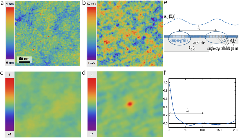
Transmission Electron Microscopy (TEM) measurements of our NbN films (see Fig.5 in the Appendix) were able to show that the films are smooth and well crystallized, and can be viewed as a closely packed assembly of nanocrystallites of different orientations. These contiguous nanocrystals have typical lateral dimensions of about 25 nm. The characteristic film structure is also reflected in topographic scanning tunneling microscopy images, as the one presented in Fig. 1a for a nominally 2.14 nm-thick sample (=3.8 K). The film surface is very flat and the observed nanoscale structures correlate well with the nanocrystals revealed by TEM. At the same time the landscape of the sample also displays smooth inhomogeneities on a larger scale of a few tens of nanometers.
Probing the inhomogeneities with STM and STS — In order to get insight into the superconducting (in)homogeneity of these ultrathin films, we performed scanning tunneling microscopy (STM) and spectroscopy (STS) experiments. Typical results are displayed in Fig. 1. Fig. 1(a) shows a topographic map of the area under study for sample ( K). In Fig. 1(b) we report the extracted superconducting gap map at 300 mK i.e. well inside the superconducting state for the area corresponding to the topographic map of Fig. 1(a). is defined from the spectra as the peak-to-peak energy (see Fig. 6 in the Appendix for the corresponding representative spectra). In agreement with previous measurements in similar systems [17, 21], we observe spatial variations of the gap (see Fig. 1(b)) and of the integrated in-gap conductance (see Appendix). However, we reveal here for the first time that these gap variations are not correlated to the topography of the surface. Indeed, the cross-correlation map between (a) and (b) reveals the absence of correlation [see Fig. 1(c)].
In Fig. 1(d) we report the autocorrelation map of the gap map shown in Fig. 1(b). It allows us to extract both the typical size of domains of constant gap values, hereafter called supergrains, and the typical distance between the centers of such adjacent supergrains. The radial profile extracted from the center of the autocorrelation map is shown in Fig. 1(f), featuring a correlation length of about 100 nm and a typical domain size of about . This is more than ten times larger than the size of the microstructural grains nm (see Fig. 1(e) depicting the relevant lengths scales). Above the global critical temperature these inhomogeneities persist, as well as a gap-like feature called pseudogap. In addition, our measurements reveal that the energy integrated in-gap conductance maps at 300 mK and at 4.2 K, performed on the same area of Fig. 1(a) are correlated (see Fig. 6 in the Appendix). We deduce that at 4.2 K remains roughly the same, whilst the spectroscopic contrast between the regions changes with temperature.
By contrast, similar spectroscopic studies carried out on thicker samples ( nm, ) revealed a much more homogeneous superconducting phase [22]. Therefore, some short-scale inhomogeneity in the superconductive properties emerges for the thinner samples at a scale while the system is structurally homogeneous over the same length scale. This is consistent with predictions from Monte-Carlo simulations [19].
Analysis of the paraconductivity — In order to probe the influence of these nanoscale inhomogeneities on the superconducting thermal fluctuations, we performed transport measurements in the vicinity of and extracted the paraconductance per square , i.e., the excess conductance per square due to superconducting fluctuations in the normal state. Here, is the square conductance measured under zero magnetic field and is the normal state square conductance. The resistance per square is displayed on Fig.2 for the different samples, together with the extrapolated [(a) solid lines] or measured [(b) full symbols] resistance of the normal state. (See the methods Section for details on the determination of the normal state.)
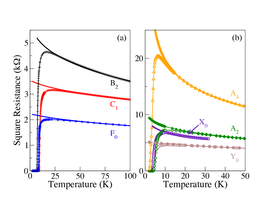
In Fig. 3(a) the variation of with the reduced temperature is shown for samples , , and : the observed critical exponent is consistent with the Aslamasov-Larkin prediction for 2D systems (AL 2D) [26] in the range , as it was reported previously for these films [25]. Remarkably, the extracted experimental AL 2D prefactor matches the theoretical one, without any adjustable parameter. This suggests that the fluctuations in this case are BCS-like, and that Maki-Thomson (MT) fluctuations [27, 28] or density-of-state (DOS) corrections[29, 30, 4] are absent or negligible.
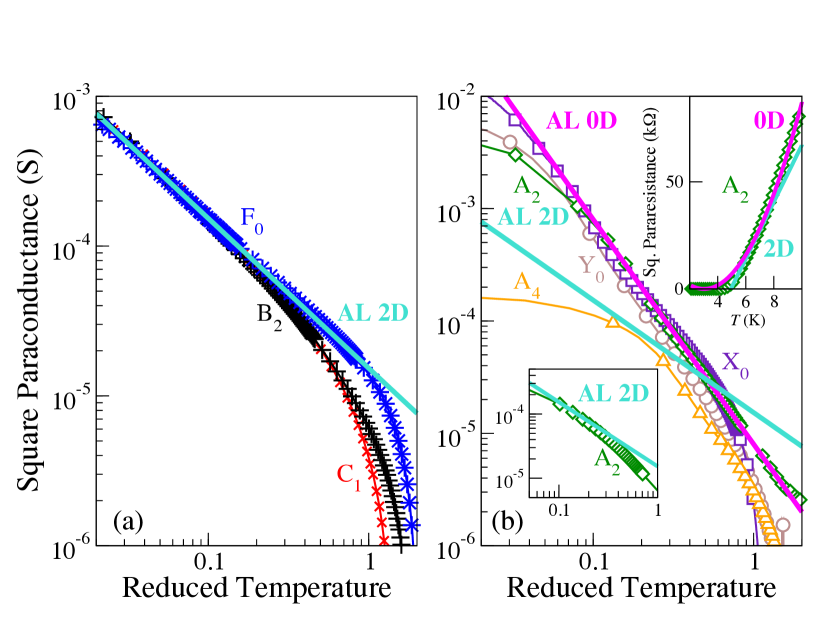
Proceeding in a similar way, we extracted the paraconductivity of the thinner samples , (aged ), and (shown as open symbols in Fig. 3(b). The AL 2D prediction is also displayed in the same Figure (purple solid line). The experimental paraconductance is found to deviate strongly from the AL 2D behavior over a significant temperature range, even when using as a free parameter, and to exhibit over a substantial range of reduced temperature a very specific law, , corresponding to 0D fluctuations, previously observed in granular materials [31, 32, 33, 34]. An empirical fitting function, for and is plotted for comparison (maroon solid line). Similar behaviors, i.e., for , and for , were found to hold for the other samples. The paraconductance data, e.g., for sample also suggests a 0D-2D crossover [see also the lower inset in Fig. 3(b)] as previously observed in [35] and discussed in [32]. We point out that the fluctuational critical temperature may differ in the two regimes, so that the crossover is more evident when the pararesistivity is plotted as a function of , without making any choice for , rather than , which depends on [see the upper inset in Fig. 3(b)].
Concerning the absence of MT terms, we stress out that, with pair breaking arising only from electron-electron interactions, MT paraconductance is less singular than the AL term in 2D [36], and even less so for 0D AL. On the other hand, the presence of a sizable pseudogap suggests that DOS corrections should be present. DOS corrections, however, lead to a decrease of the paraconductance. In our case, instead, the paraconductance in the pseudogap regime is found to be even more singular with dependence that can not be explained by DOS contribution. This clearly indicates that DOS corrections, although expected, are immaterial in this case.
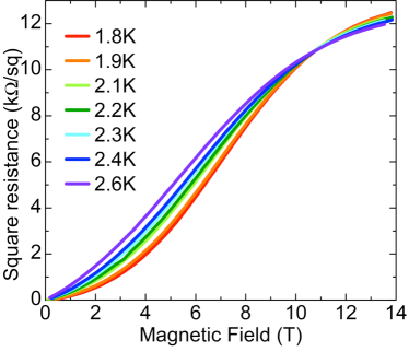
Study of the magnetic field driven transition — The above study near was complemented by the analysis of the transport properties of the thinnest samples at the transition to the normal state driven by magnetic field, well below . We found that the curves cross at a specific point (see also Fig. 8 in the Appendix for further details). Following Ref. 37, we analyzed the curves in the vicinity of this point and evidenced a scaling behavior of the type with the critical exponent (See the data in Fig. 4(a) for sample ). The occurrence of such scaling behavior, where is the only relevant scale, marks the existence of a quantum critical point (QCP) at zero temperature and for . Consequently, the exponent can be expressed as , where is the exponent that rules the variation of the spatial correlation length and is the dynamical critical exponent .
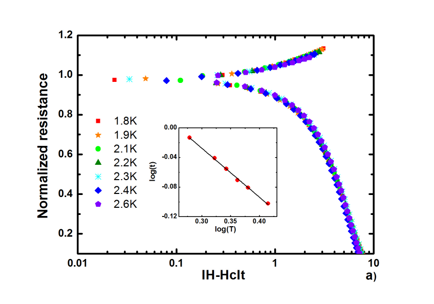
In order to extract the values of and from , similar measurements were performed at a fixed temperature, 1.9 K, for different values of the electric field, i.e., of the bias voltage across the sample [see the data for sample in Fig. 4(b)]. Here again, the curves exhibit a common crossing point corresponding to the QCP (see Fig. 9 in the Appendix). The scaling analysis in the vicinity of this point, with a scaling function of the form , yielded . Following the analysis in Refs. 37, 38, 39, we express as . The two independent determinations of and allow us to establish and . The latter is precisely the result expected, e.g., in systems with (weakly screened) long-range Coulomb interactions, while the former is consistent with a 3D classical XY model or 2D quantum XY model (with z=1). A similar analysis, performed on sample under high pulsed magnetic field allowed to evidence a plateau between 1.5K and 8K for and to extract a product of critical exponents .
Discussion
As we report in the Appendix, the coherence length exponent that leads to the observation of an anomalous power law , is consistent with a formal calculation of AL fluctuations in a 0D system. is converted into the measured paraconductance per square by means of a suitable length scale , which represents the size of the 0D fluctuating domains, in the plane parallel the film, yielding . Deducing for a value of 5.5 0.5 nm from the value of at the QCP, in agreement with extrapolated values in [25], it is possible to extract from the paraconductivity data. One finds, e.g., nm for samples ( K) and ( K), nm for sample ( K), and nm for sample . This length is in good quantitative agreement with the typical domain size extracted from STS data at 300 mK and at 4.2 K for sample ( K). This means that the length and not the real grain size sets the scale for the 0D fluctuating domains, until becomes larger than . Further theoretical investigation is necessary to understand the physical meaning of the presence of these 0D domains, that behave like smooth "supergrains". The observed behavior could actually be interpreted in terms of slower diffusion of the Cooper pairs thus increasing their lifetime on length scales smaller than . By contrast, a standard diffusive behavior is recovered at longer times and larger distances giving way to standard 2D behavior eventually ruling the transition (see the Appendix for more details).
To our knowledge, the only previous evidence in the literature of a 0D fluctuations regime in transport is for nominally granular or filamentary systems [31, 33, 34]. The novelty lies here in the observation of such behavior in a compound where the inhomogeneity arises in a “mild” way: The films are far from granularity because the 0D behavior does not occur on the small scale of the crystallites, but rather on the larger typical scale , comparable to the correlation length inferred from STS. The emergent (as opposed to the structural) character of the 0D regions is also suggested by the lack of any correlation [see Fig. 1(c)] between the inhomogeneous domains observed with STS [Fig. 1(b)] and the large-scale structural disorder observed in the topography of the crystallite ensemble [Fig. 1(a)].
For the superconducting transition to be probed in transport, the 0D fluctuations regime has to finally evolve to higher-dimensional behavior. Close enough to a crossover to 2D behavior must (and does) occur, when the superconducting coherence length becomes larger than and enables to couple different 0D domains, following a scenario analogous to the Lawrence-Doniach description for lamellar materials [40, 32]. As a matter of fact, the 0D-2D crossover is visible for sample ( nm), as well as for the sample ( nm). Please see the insets of Fig. 3. However, we propose here a different physical explanation for this crossover. We start with an expression of the AL paraconductivity in dimensions (see details in the Appendix):
| (1) |
with a suitable "density of states" (weighted with current vertices) . Setting , the standard AL result is found for , corresponding to diffusion of fluctuating Cooper pairs in two dimensions. However, if
| (2) |
corresponding to a slowing-down of the diffusion of fluctuating Cooper pairs above a threshold , a 0D behavior
| (3) |
is found for . A comparison with the formal extrapolation of AL fluctuations to yields . For , the standard 2D AL paraconductivity is recovered.
Finally, at even lower temperature (below the 2D AL transition temperature), the system might be governed by percolation physics or, alternately, by Berezinski-Kosterlitz-Thouless behavior. This behavior, if any, should occur on a very restricted range of temperature, because our measurements always display the paraconductivity of standard gaussian fluctuations. If the bosonic scenario was applicable to our films, the transition should be ruled by dephasing of the pairs and paraconductivity should mirror the characteristics of the vortex fluctuations in the BKT transition [41]. So, at first sight, our findings seem at odds with the existence of a pseudogap on the normal side of the transition as is well established in the literature and can be seen in the conductance maps and spectra in the supplementary material, and which is usually ascribed to the strong localization of Cooper pairs [23, 18]. Our work suggests a different explanation. The diffusion slowing down of the fluctuating Cooper pair in the "supergrains" increases their lifetime. This might occur either because they locally find a more suitable environment, like, e.g., a locally higher , or, conversely, because they display an increased tendency to localize for those wavevectors corresponding to the largest inhomogeneities. This second possibility seems more likely because our fits suggest that the 0D critical temperature (i.e. the “local” critical temperature) is slightly lower than the 2D large-scale . The incipient localization and diffusion slowing down of the Cooper pairs seems to have a sizable effect on depressing the density of state at the Fermi level, thus suggesting the possibility of a substantial fluctuational pseudogap [24] [29].
The magnetic-field driven transition at low temperature can be interpreted as magnetic field-induced dephasing of the 0D supergrains thereby accounting for the critical exponents of an XY model in 2+1 dimensions, the additional "1" coming from the dynamical critical index . The value is pertinent, e.g., to systems with (weakly screened) long-range Coulomb interactions [42]. It is also consistent with numerical calculations based on a Boson-Hubbard model [43]. Similar values for were observed in Bi [39] or NbSi [44] amorphous thin films, whereas a large number of studies of the SIT point towards a different universality class with [45, 38, 46, 47], a critical exponent consistent with classical percolation. Our findings are therefore in agreement with a picture of phase fluctuating 0D supergrains coupled à la Josephson, for the magnetically driven transition.
The question arises of the origin of the electronic inhomogeneities. Indeed, while the structural small scale inhomogeneity associated to the structural grains (25 nm) appears to be irrelevant, we deal with three larger scales over distances of tens of nanometers ( nm): a) the electronic inhomogeneity of the pseudogap seen by STS [Fig. 1(b)]; b) the scale of the 0D AL behavior seen in transport, and c) the topographic smooth landscape [Fig. 1(a)]. Although the scale b) is obtained from transport and cannot be easily connected to a spatial structure, it is quite tempting to associate the electronic scales of pseudogap and 0D transport to the scale on which Cooper pairs tend to localize (before they eventually condense on the infinite scale of the 2D transition). On the other hand, the fact that there is no correlation between the topographical map and the superconducting gap map proves that the structure is not responsible for the gap inhomogeneities in a trivial way. i.e. it is not some local parameter variation (for instance thickness or stoichiometry) that induces a locally-correlated variation of the superconducting properties. This does not mean that disorder or structural inhomogeneities are irrelevant. They are most probably relevant, but in a complex manner such as, for instance, disorder is relevant for localization but localization length is not simply the distance between impurities.
In any case the main result of our work is that a 0D physics is found to spontaneously emerge in transport measurements on the same length scales as the length scale for the superconducting inhomogeneities, much larger than the structural crystallites, indicating that this structural complexity has an electronic counterpart producing anomalous diffusion of the Cooper pairs.
Conclusion
The emergence of (glassy) inhomogeneous superconducting phases out of homogeneously disordered films has been proposed both theoretically [12, 16, 19] and measured experimentally [18, 22, 21]. Our STS measurements have evidenced electronic inhomogeneities with typical correlation length ( nm) and typical domain size in the superconducting state below and in the superconducting fluctuations above in NbN ultrathin films. These inhomogeneities, which are much larger than the structural grains of the film made of nanometer-sized nanocrystals, correspond to simultaneous spatial variations of the energy of the superconducting gap and of the energy-integrated in-gap conductance, and are found to become dominating for the thinner samples, where they strongly affect the superconductive thermal fluctuations. Specifically, we have shown that, for films with nominal thickness nm or , these inhomogeneities are associated with specific exponents in the dependence of the gaussian superconducting fluctuations with reduced temperature. These exponents are consistent with AL fluctuations confined into 0D supergrains of size . On the other hand, at low temperature, the analysis of the magnetic field driven transition is consistent with a 2D quantum XY model, which is also evocative of 0D supergrains coupled à la Josephson. In this regime, the Cooper pairs are tightly bound and the transition is ruled by supergrain dephasing, in contrast to the transition at finite temperature where AL amplitude fluctuations are instead observed.
We propose that, above , diffusion slowing down of the Cooper pairs in the supergrains increases their lifetime and leads to a depression in the density of states at the Fermi level, yielding a fluctuational pseudogap. The origin of these inhomogeneities as well as of this anomalous diffusion process is still to be investigated. In any case, this work appeals for a new theoretical microscopic description for this peculiar state of matter, with interplay of localization and pairing, intermediate between the Fermi and the Bose insulators paradigms.
Methods
Scanning tunneling spectroscopy The electronic inhomogeneities in the superconducting state were probed by using scanning tunneling spectroscopy (STS) at 300 mK or 4.2 K and establishing full STS grids of typically 256256 resolution over a 300300 nm2 area. The tunneling conductance spectra were obtained by numerical derivation of the data. The conductance maps shown in Fig. 6 of the Appendix were obtained by integrating in energy the individual conductance spectra in an energy range of meV. The radial profile shown in Fig. 1(f), extracted from the autocorrelation map [Fig. 1(d)] of the gap map [Fig. 1(b)], is the circular average of all profiles passing through the center of the autocorrelation map. The measurements were performed with a Pt/Ir tip.
Transport measurements Transport measurements were carried out by means of a standard four-probe technique in a 14 T Quantum Design PPMS (Physical Properties Measurement System). Resistance data was extracted using either a dc current or an ac current at 17 Hz. Four-probe contacts were made by directly bonding Al wires to the NbN films. Six different samples were experimentally analyzed corresponding to different thicknesses: 2.10 nm (), 2.14 nm (), 2.16 nm (, or , after aging), 2.33 nm (), 2.5 nm () and 2.9 nm (). The resistivity was measured as a function of temperature with various magnetic field ranging from 0 T to 14 T and for sample with various applied currents in the vicinity of the QCP.
The critical temperature was determined by using the extrapolation to zero resistance of the tangent at the inflection point of the resistance versus temperature curve. See the values in Table 1 of the Appendix.
High magnetic field measurements were performed at LNCMI (Toulouse) on sample , using pulsed fields up to 55 T. The ac resistance was measured using four probe technique at a frequency of 50 kHz. This was used to perform scaling analysis on sample at the vicinity of the QCP.
In order to determine the paraconductance contribution, one needs to extract the normal state conductance. For samples , and , that were close enough to the insulating transition, so that the normal state was recovered under a perpendicular 14 T magnetic field, we identified with . For the thicker samples , and , the normal state was not recovered under 14 T and we extrapolated the normal state from the high-temperature data (typically between 80K ad 150K) using the same fitting law that worked for the 14 T resistance of the thinner samples, but with different parameters, namely , with . (For , that was measured in situ inside the STM cryostat, a similar extrapolation was used for the normal state.) This extrapolation may induce an error on the absolute amplitude of , but not on the exponent governing the temperature dependence of the divergent term in at , since no divergence at is present in the normal state conductance nor in its fitting law.
I Acknowledgments
This work has been supported by a SESAME grant from Region Ile-de-France. Collaboration with Università di Roma La Sapienza was supported by CNRS through a PICS program (S2S) and by a Joliot grant from ESPCI ParisTech. The work at INSP was supported by the Emergence-UPMC program. We acknowledge the support of the LNCMI-CNRS, member of the European Magnetic Field Laboratory (EMFL).
APPENDIX
II Sample fabrication and characterisation
The NbN films were grown at Karlsruhe Institute of Micro and Nanoelectronic Systems, on the optically polished side of sapphire substrates by means of dc reactive magnetron sputtering of a pure Nb target in an gas mixture as described in Ref. [25]. The deposition process was optimized in order to provide the highest transition temperature.
The thickness was evaluated during the deposition of NbN at the Karlsruhe Institute of Micro and Nanoelectronic Systems, by time of exposure of the substrate and measurement of the deposition rate. Figure 5 shows a high-resolution transmission electron microscopy image of a 2.33 nm-thick NbN film. The atomic rows of the sapphire substrate and of the NbN layers are clearly visible. The NbN film consists of nanocrystals of typical size of approximately 2-5 nm, linked together by crystalline boundaries.
Both the chemical analysis performed across the film and the atomic force microscopy (AFM) measurements indicated that an oxide layer (presumably ) is present on top of the NbN films. This layer appears within a few minutes after exposing the film to air for the first time. The thickness of the oxide layer on newly prepared films varies in the range 0.5 to 1 nm. Further oxidation proceeds much slower. The transition temperature of samples with K was actually found to decrease with time and thermal cycling. Simultaneously, the normal-state resistance was found to increase. This fact was used experimentally to tune the superconductor/insulator transition in sample which corresponds to aged . We were able to establish that the top oxide layer is insulating and not conducting. The dependency of the STM tunneling current versus tip-sample distance shows an exponential decay whose exponent is directly linked to the effective work function of the sample. For a metallic sample, it is typically around 4eV. When an ultrathin (ie few atomic monolayers thick) insulating barrier on top of a metal is present, the effective work function is lowered (see [48]), typically by a factor of two at least. We have observed that the dependency of the tunneling current shows such a reduced work function, thus supporting the existence of an insulating oxide layer. Therefore the existence of a top metallic layer such as NbO for instance seems unlikely in our case. The effect of this oxide layer on the superconducting properties of ultra thin NbN films is discussed in more details in [22].
III Scanning tunneling spectroscopy (STS) data
We present in Fig.6a) and b) the representative tunneling spectra measured at 300 mK and 4.2 K on the area of interest shown in Fig. 1a of the main text. The blue spectra are measured on the lower gap areas (blue areas) of the gap map presented in Fig. 1b of the main text, while red spectra are measured on larger gap areas of Fig. 1b.
It is seen that a spatially varying pseudogap is measured at 4.2 K, having the characteristic energy scale of the superconducting gap measured at low temperature. Figs. 6c) and d) present conductance maps integrated in the energy range of the low-temperature superconducting gaps, at 300 mK (c) and at 4.2 K (d). It is clear from this figure that both superconducting correlations and superconducting inhomogeneities persist above . In addition, our analysis shows that these two conductance maps c) and d) measured over the same topographic area are strongly correlated. This result can be seen in Fig. 6e) where the cross-correlation map between 6c) and 6d) is plotted. This proves that the inhomogeneities in the energy gap value below and in the pseudogap features above are strongly spatially correlated. Furthermore, the radial profile shown in Fig. 6f), extracted from a circular average of the cross-correlation map e), allows us to infer that the characteristic correlation length of these inhomogeneities at 4.2 K is comparable to the one seen at 300 mK, of size about 100 nm. We have also performed STS measurements on sample at higher temperature so well in the 0D regime (around 7K) which show similar results as the one presented in Fig. 6b) and Fig. 6d) at 4.2K. The only difference between the 7K and 4.2K data is that the spectroscopic features related to the pseudogap are smaller in amplitude at 7K. But the regions where the pseudogap is still present (corresponding to the supergrains) have the same characteristic size and spacing as at 300mK or at 4.2K.
IV Analysis of the paraconductivity: Fitting parameters for the normal state resistance
For samples , and , that were close enough to the insulating transition, so that the normal state was recovered under a perpendicular 14 T magnetic field, we identified with . The resistance of sample was measured in situ inside the STM cryostat up to 30 K, therefore the measure under 14T magnetic field could not be performed, and we extrapolated the normal state. For the thicker samples, , and , superconductivity could not be completely suppressed by a magnetic field of T. In such cases, the normal-state resistance was fitted by an expression that worked well for the thinner samples under 14 T,
| (4) |
with . We determined the parameters fitting the high-temperature resistance, typically in the range 80150 K (except for the sample , for which the range was forcedly smaller, 1030 K). The fitting parameters are found in Tab. 2.
| sample name | |||||
|---|---|---|---|---|---|
| 2.90 | 9.0 | 1390 | 8.6 | - | |
| 2.50 | 9.4 | 2370 | 9.5 | - | |
| 2.33 | 7.1 | 2450 | 7.1 | - | |
| 2.16 | 4.5 | 3150 | 4.9 | 4.4 | |
| (aged ) | 2.16 | 2.4 | 4570 | 3.0 | 2.9 |
| 2.14 | 3.8 | 3800 | 3.9 | 3.6 | |
| 2.10 | 4.3 | 2350 | 4.9 | 4.3 |
| sample name | |||
|---|---|---|---|
| 9299 | 1038 | 1.370 | |
| 5804 | 275.3 | 10.53 | |
| 3529 | 32.32 | 6.094 | |
| 2212 | 4.512 | 4.381 |
V Analysis of the paraconductivity: possible observation of a 0d-2d crossover
In Fig. 7 we plot the pararesistance as a function of temperature (and not reduced temperature ) for sample . Such plot (similar the right inset of Fig. 3b in the Article for sample ) allows to visualize both the 0D AL (quadratic) regime and the 2D (linear) regime closer to . Since the two regimes are characterized by different “fluctuational” critical temperatures, they cannot be both visualized with a single choice of in the reduced temperature . Such 0D-2D crossover was indeed observed in all thinner samples , , and .
VI Study of the quantum critical region
In Fig. 8 are displayed the isothermal resistance versus magnetic field curves for different temperatures. The curves for temperatures between 1.8 K and 2.6 K exhibit a common crossing point, at T and k, corresponding to the quantum critical point. For these measurements, the current and voltage values across the sample were very low and the curves were found to be insensitive to amplitude variations of the current bias.
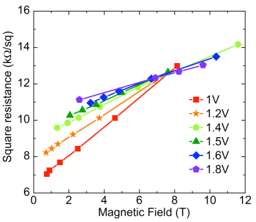
In Fig. 9 are displayed the isopotential resistance versus magnetic field curves for different values of the voltage applied across the sample, corresponding to different values of the electric field. The measurements were performed at 1.9 K. As for the isothermal curves, the isopotential curves are found to cross in a single point. These curves were then used for scaling analysis as described in the Article.
VII Theoretical analysis of paraconductivity
VII.1 Zero dimensional Aslamazov-Larkin (AL) fluctuations
To discuss AL paraconductivity, we assume overall isotropy (at least in the average) and start from the expression [26, 49]
| (5) |
that reproduces the standard AL result in dimensions with being the relaxation rate for each mode . is the coherence length and , being the critical temperature seen by the fluctuating Cooper pairs (which may differ from the actual critical temperature, in the presence of crossover phenomena). The above formula is rather general [50], although the expression of may change depending on the microscopic theory, and the expression , with a dimensionless prefactor not necessarily equal to one, might be used. However, for definiteness, we adopt henceforth the standard definition of .
Since only depends on , the angular integration factors out and one obtains
| (6) |
where is the surface of the unitary sphere in dimensions and is the Euler gamma function. Exploiting the expression of one obtains
| (7) |
When , inherits the singularity of , so that , and
| (8) |
i.e., there exists a well defined limit of the AL paraconductivity as , that scales with , and qualitatively agrees with the behavior observed in the thinnest NbN films. This result is converted into the measured conductance per square, dividing it by the square of a suitable length scale , related with the size of the fluctuating (nano)domains,
| (9) |
However, although the supergrains may behave as quantum dots, closer to the system is two-dimensional, the supergrains are coupled, and the paraconductive fluctuations must cross over to . The formal limit does not allow for a description of this crossover and the identification of the relevant length scales. A crucial remark of Ref. [49] is that the AL theory can be cast in an even more general form, introducing a suitable weighted density of states,
| (10) |
which allows to write the paraconductivity in the form
| (11) |
The standard AL result is recovered with
| (12) |
yielding
| (13) |
We argue that the observed 0D-2D crossover stems from a different form of , that results from the supergrains (endowed with an internal structure) being connected in a 2D network. In the following we thus set . The standard 2D AL result is found for , corresponding to diffusion of fluctuating Cooper pairs in two dimensions. If instead , for , and , for , which describes a slowing-down of the diffusion of fluctuating Cooper pairs above a threshold (e.g., corresponding to trapping of the fluctuations within the supergrains), the paraconductivity is
| (14) |
which recovers the 2D behavior for , while for
| (15) |
mimicking the 0D behavior at higher temperature. A comparison with the formal extrapolation of AL fluctuations for yields . As a matter of fact, the 0D-2D crossover is clearly visible for sample ( nm) for which a much greater number of points was taken in the vicinity of the transition, as well as for the sample ( nm), but also for and . Eventually, at temperatures below the 2D AL regime, the system may be governed by percolation physics or, alternatively, by Berezinski-Kosterlitz-Thouless behavior.
A rough estimate gives , where is the temperature dependent correlation length that diverges at the transition. Then, the 0D-2D crossover takes place at a temperature such that . A comparison with the formal 0D limit of the AL theory allows us to identify , hence the size of the supergrains .
Références
- [1] Gol’tsman G.N., Okunev O., Chulkova G., Lipatov A., Semenov A., Smirnov K., et al. Picosecond superconducting single-photon optical detector. Applied Physics Letters, 79, 705 (2001).
- [2] Hofherr M., Rall D., Ilin K., Siegel M., Semenov A., Hübers H.W., et al. Intrinsic detection efficiency of superconducting nanowire single-photon detectors with different thicknesses. Journal of Applied Physics, 108, 014507 (2010).
- [3] Goldman A.M. and Marković N. Superconductor-Insulator Transitions in the Two-Dimensional Limit. Physics Today, 51, 39 (1998).
- [4] Beloborodov I., Lopatin A., Vinokur V., and Efetov K. Granular electronic systems. Reviews of Modern Physics, 79, 469-518 (2007).
- [5] Finkel’Shtein A.M. Superconductivity-transition temperature in amorphous films. Pisma v Zhurnal Eksperimentalnoi i Teoreticheskoi Fiziki, 45, 37-40, (1987).
- [6] Valles J.M., Jr, Dynes R.C., and Garno J.R. Electron tunneling determination of the order-parameter amplitude at the superconductor-insulator transition in 2D. Physical Review Letters, 69, 3567-3570 (1992).
- [7] Fisher M.P.A, Grinstein G., and Girvin S.M. Presence of quantum diffusion in two dimensions: Universal resistance at the superconductor-insulator transition. Physical Review Letters, 64, 587-590, (1990).
- [8] Fisher M.P.A. Quantum phase transitions in disordered two-dimensional superconductors. Physical Review Letters, 65, 923-926(1990).
- [9] Seibold G., Benfatto L., Castellani C., and Lorenzana J. Superfluid Density and Phase Relaxation in Superconductors with Strong Disorder. Physical Review Letters, 108, 207004 (2012).
- [10] M Feigel’man, L Ioffe, V Kravtsov, and E Yuzbashyan. Eigenfunction Fractality and Pseudogap State near the Superconductor-Insulator Transition. Physical Review Letters, 98, 027001(2007).
- [11] Feigel’man M.V., Ioffe L.B., Kravtsov V.E., and Cuevas E. Annals of Physics. YAPHY, 325,1390-1478 ( 2010).
- [12] L B Ioffe and Marc Mézard. Disorder-Driven Quantum Phase Transitions in Superconductors and Magnets. Physical Review Letters, 105, 037001 (2010).
- [13] Hollen S.M., Fernandes G.E., Xu J.M., and Vallès J.M. Collapse of the Cooper pair phase coherence length at a superconductor-to-insulator transition. Physical Review B, 87,054512(2013).
- [14] Stewart M.D., Yin A., Xu J.M., and Valles J.M. Superconducting pair correlations in an amorphous insulating nanohoneycomb film. Science, 318, 1273-1275 (2007).
- [15] Kopnov G., Cohen O., Ovadia M., Lee K.H., Wong C.C., and Shahar D. Little-Parks Oscillations in an Insulator. Physical Review Letters, 109, 167002 (2012).
- [16] Lemarié G., Kamlapure A., Bucheli D., Benfatto L., Lorenzana J., Seibold G., et al. Universal scaling of the order-parameter distribution in strongly disordered superconductors. Physical Review B, 87, 184509 ( 2013).
- [17] Sacépé B., Chapelier C., Baturina T.I., Vinokur V.I. , Baklanov M.R., and Sanquer M. Disorder-Induced Inhomogeneities of the Superconducting State Close to the Superconductor-Insulator Transition. Physical Review Letters, 101, 157006 (2008).
- [18] Sacépé B., Dubouchet T., Chapelier C., Sanquer M., Ovadia M., Shahar D., et al. Localization of preformed Cooper pairs in disordered superconductors. Nature Physics, 7, 239-244 (2011).
- [19] Bouadim K., Loh Y.L., Randeria M. and Trivedi N. Single- and two-particle energy gaps across the disorder-driven superconductor–insulator transition. Nature Physics, 7, 884-889 (2011).
- [20] Trivedi N., Loh Y.L., Bouadim K., and Randeria M. Emergent granularity and pseudogap near the superconductor-insulator transition. Journal of Physics: Conference Series, 376, 012001 ( 2012).
- [21] Kamlapure A., Das T., Ganguli S.C., Parmar J.B., Bhattacharyya S., and Raychaudhuri P. Emergence of nanoscale inhomogeneity in the superconducting state of a homogeneously disordered conventional superconductor. Scientific Reports, 3 , 2979 (2013).
- [22] Noat Y., Cherkez V., Brun C, Cren T., Carbillet C., Debontridder F., et al. Unconventional superconductivity in ultrathin superconducting NbN films studied by scanning tunneling spectroscopy. Physical Review B, 88, 014503 (2013).
- [23] Sacépé B., Chapelier C., Baturina T.I., Vinokur V.I. , Baklanov M.R., and Sanquer M. Pseudogap in a thin film of a conventional superconductor. Nature Communications, 1,140 (2010).
- [24] Abrahams E., Redi M., and Woo J. Effect of Fluctuations on Electronic Properties above the Superconducting Transition. Physical Review B, 1, 208-213 (1970).
- [25] Semenov A., Günther B., Böttger U., Hübers H.W., Bartolf H., Engel A., et al. Optical and transport properties of ultrathin NbN films and nanostructures. Physical Review B, 80, 054510 (2009).
- [26] Aslamasov L.G. and Larkin A.I. The influence of fluctuation pairing of electrons on the conductivity of normal metal. Physics Letters A, 26, 238-239(1968).
- [27] Maki K. Critical fluctuation of the order parameter in a superconductor. I. Progress of Theoretical Physics, 40, 193-200 (1968).
- [28] Thompson R.S. Microwave, flux flow, and fluctuation resistance of dirty type-II superconductors. Physical Review B, 1, 327(1970).
- [29] Beloborodov I.S. and Efetov K.B. Negative Magnetoresistance of Granular Metals in a Strong Magnetic Field. Physical Review Letters, 82, 3332-3335 (1999).
- [30] Beloborodov I.S., Efetov K.B., and Larkin A.I. Magnetoresistance of granular superconducting metals in a strong magnetic field. Physical Review B, 61, 9145-9161 (2000).
- [31] Kirtley J., Imry Y., and Hansma P.K. Fluctuation-Induced Conductivity Above the Critical Temperature in Small-Particle Arrays. Journal of Low Temperature Physics, 17, 247 (1974).
- [32] Deutscher G. , Imry Y., and Gunther L. PhysRevB.10).4598. Physical Review B, 10, 4598 (1974).
- [33] Civiak R.I., Elbaum C., Nichols L.F., Kao H.I., and Labes M.M. Fluctuation-Induced Conductivity and Dimensionality in Polysulfur Nitride. Physical Review B, 14, 5413-5421 (1976).
- [34] Wolf S. and Lowrey W.H. Zero Dimensionality and Josephson Coupling in Granular Niobium Nitride. Physical Review Letters, 39, 1038-1041 (1977).
- [35] Belevtsev B.I. and Komnik Y.F. Superconducting fluctuations above Tc in quench-condensed hydrogen-doped indium films: transition from two- to zero-dimensional. Fis. Nisk. Temp., 9, 581(1983).
- [36] Reizer M.Y. Fluctuation conductivity above the superconducting transition: Regularization of the Maki-Thompson term. Physical Review B, 45,12949 (1992).
- [37] Sondhi S.L. , Girvin S.M., Carini J.P., and Shahar D. Continuous quantum phase transitions. Reviews of Modern Physics, 69, 1-19(2012).
- [38] Yazdani A. and Kapitulnik A. Superconducting-insulating transition in two-dimensional a-MoGe thin films. Physical Review Letters, 74, 3037-3040 (1995).
- [39] Marković N., Christiansen C., Mack A.M., Huber W.H., and Goldman A.M. Superconductor-insulator transition in two dimensions. Physical Review B, 60, 4320 (1999).
- [40] Lawrence W.E. and Doniach S. Theory of layer structure superconductors. Proc. 12th Int. Conf. on Low Temp. Phys., 361 (1971).
- [41] Halperin B.I. and Nelson D.R. Resistive Transition in Superconducting Films. Journal of Low Temperature Physics, 36, 599-616 (1979).
- [42] Herbut I. Quantum Critical Points with the Coulomb Interaction and the Dynamical Exponent: When and Why z=1. Physical Review Letters, 87,137004 (2001).
- [43] Kisker J. and Rieger H. Bose-glass and Mott-insulator phase in the disordered boson Hubbard model. Physical Review B, 55, R11981 (1997).
- [44] Aubin H., Marrache-Kikuchi C., Pourret A., Behnia K., Bergé L., Dumoulin L., et al. Magnetic-field-induced quantum superconductor-insulator transition in . Physical Review B, 73, 094521 (2006).
- [45] Hebard A.F. and Paalanen M.A. Magnetic-field-tuned superconductor-insulator transition in two-dimensional films. Physical Review Letters, 65, 927-930 (1990).
- [46] Kapitulnik A., Mason N., Kivelson S., and Chakravarty S. Effects of dissipation on quantum phase transitions. Physical Review B, 63, 125322 (2001).
- [47] Steiner M. and Kapitulnik A. Superconductivity in the insulating phase above the field-tuned superconductor–insulator transition in disordered indium oxide films. Physica C: Superconductivity, 422, 16-26 (2005).
- [48] Hans-Christoph Ploigt, Christophe Brun, Marina Pivetta, François Patthey, and Wolf-Dieter Schneider Local work function changes determined by field emission resonances : NaCl?Ag(100). Phys. Rev. B, 76, 195404 (2007).
- [49] S Caprara, M Grilli, B Leridon, and J Lesueur. Extended paraconductivity regime in underdoped cuprates. Physical Review B, 72 104509 (2005).
- [50] S Caprara, M Grilli, B Leridon, and J Vanacken. Paraconductivity in layered cuprates behaves as if due to pairing of nearly free quasiparticles. Physical Review B, 79, 024506 (2009).
VIII Author contribution
The samples were made by KI. The TEM experiments were performed by DD and LL. The transport measurements were proposed
by BL and carried out by CC. The high magnetic field measurement were proposed by BL and carried out by CC, WT and BV.
The STS measurement were proposed by DR, TC and CB and carried out by CC, CB, TC, FD and DR. The analysis of the
transport data was done by CC, BL, SC and MG and of tunneling data by CC, TC and CB. The 0D AL paraconductivity
was proposed by BL and calculated by SC and MG. The paper was written by BL, SC, MG and CB. All authors discussed
the results and commented on the manuscript.