Edge states, spin transport and impurity-induced local density of states in spin-orbit coupled graphene
Abstract
We study graphene which has both spin-orbit coupling (SOC), taken to be of the Kane-Mele form, and a Zeeman field induced due to proximity to a ferromagnetic material. We show that a zigzag interface of graphene having SOC with its pristine counterpart hosts robust chiral edge modes in spite of the gapless nature of the pristine graphene; such modes do not occur for armchair interfaces. Next we study the change in the local density of states (LDOS) due to the presence of an impurity in graphene with SOC and Zeeman field, and demonstrate that the Fourier transform of the LDOS close to the Dirac points can act as a measure of the strength of the spin-orbit coupling; in addition, for a specific distribution of impurity atoms, the LDOS is controlled by a destructive interference effect of graphene electrons which is a direct consequence of their Dirac nature. Finally, we study transport across junctions which separates spin-orbit coupled graphene with Kane-Mele and Rashba terms from pristine graphene both in the presence and absence of a Zeeman field. We demonstrate that such junctions are generally spin active, namely, they can rotate the spin so that an incident electron which is spin polarized along some direction has a finite probability of being transmitted with the opposite spin. This leads to a finite, electrically controllable, spin current in such graphene junctions. We discuss possible experiments which can probe our theoretical predictions.
pacs:
73.20.-r, 73.40.-c, 73.63.-bI Introduction
The last several years have witnessed a tremendous amount of research on graphene, both theoretical and experimental been08 ; neto09 ; rev3 ; rev4 ; rev5 . Graphene is a two-dimensional hexagonal lattice of carbon atoms in which the electrons hop between nearest neighbors. At half-filling, the spectrum is gapless at two points (called and ) in the Brillouin zone, and the energy-momentum dispersion around both those points has the Dirac form , where is the Fermi velocity. The Dirac nature of the electrons gives rise to many interesting properties of this material, such as Klein tunneling through a barrier katsnelson06 , novel effects of crossed electric and magnetic fields lukose07 , qualitatively different transport characteristics of superconducting graphene junctions beenakker1 ; bhattacharjee06 ; beenakker2 ; maiti07 , possibility of multichannel Kondo physics ksen3 ; kond1 ; kond2 ; kond3 ; kond4 , interesting power laws in the local density of states (LDOS) induced by an impurity cheianov06 ; mariani07 ; bena08 ; bena09 , and atomic collapse in the presence of charged impurities levitov07 .
Recent years have also seen extensive research on topological systems hasan ; qi . These systems have a bulk spectrum which is gapped; however, the topological properties of the bulk states ensure, via bulk-boundary correspondence, that the boundary (namely, the edge for a two-dimensional system like graphene) has gapless states. The number of species of gapless states is given by a topological invariant which can be calculated from the bulk spectrum. While pristine graphene is gapless in the bulk and is therefore not topological, it can be made to undergo a transition to a topological phase with a non-zero Chern number by adding an appropriate conserving spin-orbit coupling (SOC) kane05 . Experimentally a SOC may be induced in graphene in various ways, such as by placing it in proximity to a three-dimensional topological insulator such as kou13 ; zhang14 or by functionalizing it with methyl zollner15 . Two models of SOC have been discussed in the literature: Kane-Mele kane05 and Rashba dutreix14 . The Kane-Mele type opens a gap and makes the system topological while the Rashba type does not open a gap and therefore does not make it topological; consequently, in this work, we shall deal mostly with the former type of SOC. In addition, it is also interesting to consider the effects of an effective magnetic field with a Zeeman coupling to the spin of the electron. Such a coupling can arise if a ferromagnetic material is placed in proximity to the graphene haugen08 ; yang13 ; song15 ; the magnetization of the ferromagnetic material will have only a Zeeman coupling to the electron spin (no orbital coupling) provided that the direction of the magnetization lies in the plane of the graphene. To the best of our knowledge, edge states, impurity effects, and spin transport in systems constituting spin-orbit and Zeeman coupled graphene have not been studied in detail earlier.
In this work, we shall study the nature of edge states, the effects of magnetic and non-magnetic impurities, and spin transport in junctions involving spin-orbit coupled graphene both in the presence and absence of a Zeeman coupling term. The pristine graphene, in our work, will be modeled by a tight-binding lattice Hamiltonian with nearest neighbor hopping on a hexagonal lattice neto09
| (1) |
where the sum over goes over the nearest neighbors, the hopping amplitude , the nearest neighbor spacing is , and denotes the spin component in, say, the direction. (We will set and unless mentioned otherwise). The hexagonal lattice has unit cells which consist of two sites; we denote the upper and lower sites, belonging to sublattices and , as and respectively. We introduce the Pauli matrices with denoting sites on the and sublattices respectively. The midpoint of a unit cell labeled as is located at , where take integer values. The spanning vectors of the lattice are and . The reciprocal lattice vectors can be chosen to be and . As is well-known, such a model leads to an energy dispersion where
The two bands touch each other at two inequivalent points; these are the well-known and with wave vectors . Around these points, the effective low-energy continuum theory of graphene electrons takes the form of a -dimensional Dirac Hamiltonian with
| (3) |
where is the Fermi velocity, at respectively (these are called valleys), and denote eight-component electron annihilation operators with the components corresponding to sublattice (), valley (), and spin () degrees of freedom. Equation (3) is the Dirac Hamiltonian and the dispersion is given by , with a four-fold degeneracy due to the valley and spin degrees of freedom.
The presence of the SOC, taken to be of the Kane-Mele type, and the Zeeman term arising out of proximity to a magnetic strip will be modeled at a lattice level by
| (4) | |||||
| (5) |
where denotes the strength of the SOC, the sum over goes over next-nearest neighbors, if the electron makes a left (right) turn to go from site to through their common nearest neighbor, and we have taken the vector , which measures the strength of the effective Zeeman field, to include factors like the coupling to the magnetization of a proximate ferromagnetic material and the Bohr magneton. It is easy to see that Eqs. (4) and (5) along with Eq. (1), lead to the continuum Hamiltonian near the Dirac points
| (6) |
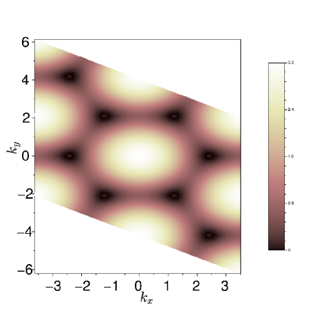
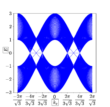
where . The energy-momentum dispersion following from Eqs. (1), (4), and (5) is shown in Fig. 1. In what follows, we shall use Eqs. (1), (4), and (5) for all numerical and analytical computations done at the lattice level and use Eq. (6) for analyzing the continuum Dirac theory for the system.
The main results that we obtain from such an analysis are the following. First, we study the edge states between pristine graphene (Eq. (1)) and graphene with SOC (Eq. (4)) and demonstrate the existence of robust chiral edge modes provided that they are separated by a zigzag edge. No such modes exist for an armchair edge. This result is in sharp contrast to the edge modes between graphene with SOC and vacuum studied earlier kane05 ; lado15 where such modes exist both for armchair and zigzag edges. We also show via an exact analytical solution that the robustness of these edge states, in spite of the presence of the gapless pristine graphene, is due to the fact that the characteristic decay length of these modes vanishes in the limit (or ) ; this behavior is in contrast to the usual divergence of the decay length edge modes with vanishing gap in the bulk. Second, we study spin-orbit coupled graphene in the presence of both single and distributed impurity (impurities) in the weak coupling limit using a -matrix formalism. We compute the energy resolved LDOS and use it to show that the width of the peaks in the Fourier transform of the LDOS provide a direct signature of the magnitude of the SOC. We also study a specific set of distributed impurities and show that the corresponding LDOS reveals a destructive interference effect which provides a direct signature of the Dirac nature of graphene electrons. Finally, we study the effect of magnetic impurities on the LDOS and show that they result in a much weaker change in LDOS as compared to charged impurities. Third, we study junctions of graphene with SOC in the form of both Kane-Mele (Eq. (4)) and a Rashba term given by , both in the presence and absence of , with pristine graphene. We show that such junctions are necessarily spin active in the sense that electrons of a definite spin approaching a junction may reflect from it with a different direction of the spin. We also demonstrate that this property of graphene junctions may be used to generate finite, electrically controllable, spin currents and thus can provide a starting step towards applications of such junctions in spintronics. We note that, to the best of our knowledge, the presence of robust edge states, the use of LDOS in the presence of impurities to estimate the strength of the SOC, and the spin active nature of graphene junctions leading to finite, electrically controllable, spin currents in spin-orbit coupled graphene junctions have not been discussed in the literature. We also note that some aspects of Kane-Mele SOC, edge states and spin transport have been studied recently in buckled honeycomb systems such as silicene, germanene and stanene rachel14 ; liu11 ; we expect our analysis demonstrating spin active junctions and leading to electrically controllable spin currents to hold for these materials as well (with minor modifications to take into account the gapped Dirac spectrum of these materials).
The plan of the paper is as follows. In Sec. II, we discuss the physics of the edge states in graphene. This is followed by a discussion of the LDOS due to the presence of an impurity (impurities) in spin-orbit coupled graphene in Sec. III. Next, we discuss the spin active nature of graphene junctions in Sec. IV and compute the spin current in several possible junction geometries. Finally, we discuss possible experiments, summarize our main results, and conclude in Sec. V.
II Edge states at junction of two regions
In this section, we study localized states at the edge between pristine graphene and graphene with SOC described by Eq. (4) and demonstrate the presence of exponentially localized chiral edge states which propagate as plane wave along the edge. We will first consider a zigzag edge.
It is known that a zigzag edge which lies between pristine graphene and vacuum hosts edge states for a finite range of the momentum along the edge nakada96 ; kohmoto07 ; these are not protected by any topological symmetry since pristine graphene is gapless in the bulk. On the other hand, a zigzag edge lying between graphene with SOC and vacuum is known to have edge states which lie in the bulk gap kane05 ; these states are topologically protected since graphene with SOC of the Kane-Mele type has a non-zero Chern number for each component of the spin. (A detailed discussion of edge states in graphene can be found in Ref. lado15, ).
A system consisting of pristine graphene separated from graphene with SOC by a zigzag edge is gapless on one side. Hence if there are states on the edge, they are not expected to be topologically protected. However we will see below that for a given momentum along the edge, these states lie in the gap of the bulk states, which means they have the same momentum in both pristine graphene and graphene with SOC. Hence these edge states cannot mix with the bulk states under perturbations which conserve the momentum.
We are interested in studying states which are localized along an infinitely long zigzag edge which runs along the direction. The momentum along the edge is therefore a good quantum number. (We have absorbed the lattice spacing in the definition of ; hence is dimensionless). We will denote the wave functions as and , where the coordinate increases vertically in the direction and the coordinate increases horizontally in the direction. We assume that the wave function is a plane wave in the direction so that or depending on whether is odd or even, and or depending on whether is even or odd; this is shown in Fig. 2. We then obtain the equations (with )
| (7) |
where we have taken into account the spin of the electron . Eqs. (7) imply that we effectively have a one-dimensional system in which the site label goes from to for a finite system with sites (i.e., unit cells). Eqs. (7) will give the energy as a function of the momentum .
Eqs. (7) remain invariant under the following sets of transformations.
(i) , , and .
(ii) , and .
(iii) , , , and .
Using the above transformations and combinations of them we can understand all the symmetries of the spectra shown in Figs. 3 (a-d) below. [The transformations in (i) have a simple interpretation. The solutions of Eqs. (7) must remain invariant if the momentum is changed from to , where is one of the reciprocal lattice vectors given in Sec. I. Since the component of both the is equal to , we see that Eqs. (7) must remain the same under ].
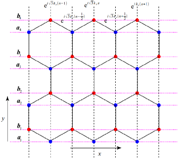
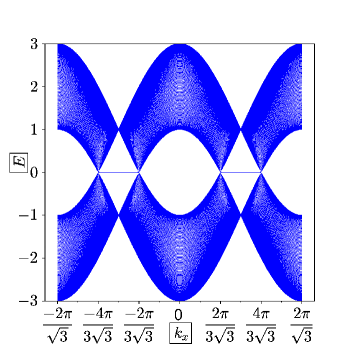
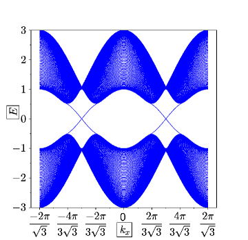
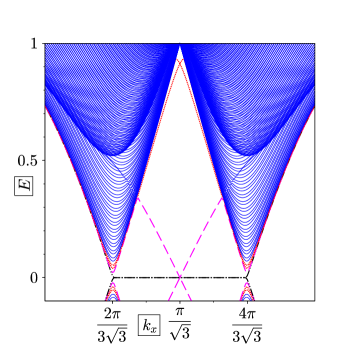
We have numerically solved Eqs. (7) for a system in which the upper half has SOC while the lower half does not; more precisely, there is a SOC between sites and (and between and ) only if are both larger than zero and . The dividing line between pristine graphene and graphene with SOC is therefore given by the zigzag edge consisting of the sites and where goes from to . The results are presented in Figs. 3 (c-d) taking . For comparison, we show in Fig. 3 (a) the spectrum for pristine graphene; apart from the gapless bulk states which are shaded blue (they almost form a continuum since the bulk momentum takes a large number of almost continuous values if is large), we see edge states which lie at exactly zero energy between the values of and and between and . Similarly, Fig. 3 (b) shows the spectrum for graphene with SOC, taking . The bulk spectrum is now gapped at the Dirac points; the gap is given by . We notice four edge states which go between the lower and upper bands, crossing zero energy at (see Fig. 1 in Ref. kane05, ). If we now look at the spectrum shown in Fig. 3 (c) for a system with a zigzag edge lying between pristine graphene and graphene with SOC, we see that all the states present in Figs. 3 (a-b) are also present here; in addition, an extra set of edge states appear which lie very close to and . These are shown more clearly in Fig. 3 (d) which is a zoomed in view of the region around .
We have analytically studied these edge states lying between pristine graphene and graphene with SOC. We find that they take a particularly simple form if ; in this case, Eqs. (7) reduce to
| (8) |
These equations admit a solution
| (9) |
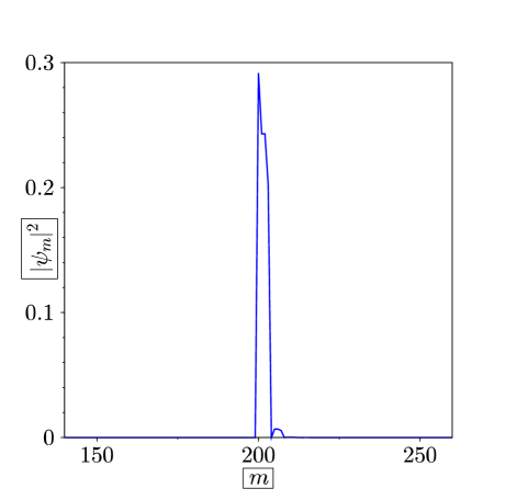
where denotes the largest integer less than or equal to , and for . (In the limit , the wave function remains non-zero only on the four sites , , , and ). Thus the energy lies within the bulk gap on the side of graphene with SOC and the wave function decays exponentially on the side of graphene with SOC and is exactly zero on the pristine graphene side; this is shown in Fig. 4 for . For small , Eq. (9) shows that the wave function decays as at a site which is unit cells away from the junction inside the region of graphene with SOC; this implies that the decay length is proportional to , where we have restored all the dimensionful parameters. Thus the decay length goes to zero as . Note that this behavior is in complete contrast with those of conventional edge states where the decay length diverges as the bulk energy gap vanishes. This indicates that while conventional edge states delocalize and merge with the continuum bulk states in the limit of vanishing gap, edge states at the boundary of graphene with SOC and pristine graphene become completely localized at the zigzag edge separating the two regimes. Away from the special values of , it is difficult to obtain analytical solutions for the edge states. However, we find numerically that for small , the edge states exist only in a small range of values of close to . The decay length of these states grows as approaches the ends of its allowed range beyond which the edge states merge with the continuum of bulk states.
It may seem surprising that such localized edge states exists even if when the system has pristine graphene everywhere. This behavior becomes obvious from Eq. (8) which admits solutions with and for any value of in this limit. Further, the presence of a state along a zigzag edge for any value of suggests an unusually large number of states, increasing linearly with , at ; this is consistent with the Van Hove singularity in the density of states of pristine graphene at those two energies neto09 .
Finally, we have numerically studied the fate of the edge states for an armchair edge. We have found that states do not appear at an armchair edge lying between pristine graphene and graphene with SOC.
We note that while graphene with SOC of the Kane-Mele type is a topological system with a bulk gap, pristine graphene is gapless in the bulk and is not a topological system. Due to the gapless nature of pristine graphene, an edge shared between it and graphene with SOC is different from an edge between topologically trivial and non-trivial insulators. In particular, the former need not host localized edge states since any low-energy states may be delocalized since bulk pristine graphene is gapless. Thus one does not need to have gapless localized states on such a boundary; however, our work shows that a zigzag edge between graphene with SOC and pristine graphene has such states while an armchair edge does not. We note that these edge states do not have topological protection in contrast to their counterparts at edges separating topologically trivial and non-trivial insulators.
It is interesting to compare our results on edge states between graphene with SOC and pristine graphene to the edge states which appear between (i) graphene with SOC and vacuum, and (ii) between pristine graphene and vacuum. These two cases have been studied extensively in the literature. It is known that edge states appear at both zigzag and armchair edges between graphene with SOC and vacuum kane05 ; sengupta06 ; jiang11 . This is because graphene with SOC is a topological system; hence states appear on any edge (zigzag or armchair) between this system and the vacuum, and all these edge states are topologically protected. On the other hand, pristine graphene is a gapless and non-topological system; hence its edges with any other system may or may not host any states. It turns out that a zigzag edge between pristine graphene and vacuum has edge states, but an armchair edge between pristine graphene and vacuum does not host any states nakada96 ; kohmoto07 ; lado15 .
We observe that Fig. 3 shows states at a zigzag edge for all the three cases discussed above. Figure 3 (a) shows edge states between pristine graphene and vacuum; these are dispersionless and lie exactly at zero energy. Figure 3 (b) shows edge states between graphene with SOC and pristine graphene; these have a dispersion and go through zero energy at two particular momenta. Finally, the top part of Fig. 3 (d) shows edge states between graphene with SOC and pristine graphene; these appear only in a small range of momentum and have a dispersion which lies close to that of the bulk states.
III Effect of localized impurity
In this section, we will study the effect that an impurity placed somewhere in graphene has on the LDOS as a function of the position and energy . By the LDOS we will mean the sum of the densities on the and sites at the unit cell labeled ; we will also sum over the electron spin. For pristine graphene this problem was studied in Refs. cheianov06, ; mariani07, ; bena08, ; bena09, ; our aim is to go beyond those papers by studying additional characteristics in LDOS due to the presence of the SO term and/or Zeeman field. In what follows, we shall carry out an analysis of the LDOS in the weak impurity potential regime where perturbation theory holds.
To compute the LDOS in this regime, we can use the standard -matrix formalism developed for pristine graphene in Refs. bena08, and bena09, . In the absence of any impurities, the density of states is given by
| (10) |
where the Green’s function is a matrix in sublattice and spin space, and is an infinitesimal positive number. Note that the LDOS in Eq. (10) is independent of as a consequence of the translation symmetry of the system in the absence of impurities. In the presence of impurities, the total Hamiltonian is given by and the LDOS is given by
| (11) |
We now consider an impurity of strength which is placed at the site of a unit cell located at with a potential given by
| (12) |
Within the -matrix formalism and to first order in perturbation theory, the change in the LDOS due to the impurity is given by
| (13) | |||||
We define the two-point real space Green’s function for graphene without impurities as
One can then write the change in the LDOS as
| (15) |
While one can numerically compute using Eqs. (LABEL:twopointg) and (15), the results seem to depend sensitively on the values of the momentum spacing and that one chooses.
In order to avoid such cutoff dependences, we have directly computed by numerically calculating with and without the impurity and then taking the difference. The calculations are carried out as follows. We consider a lattice in which the integers go from to some integer ; hence the lattice has unit cells and sites. We impose periodic boundary conditions. (There are two reasons for choosing such a boundary condition. First, it ensures that momentum is a good quantum number in the absence of an impurity. Second, we will study below the Fourier transform of the change in the local density of states produced by the impurity; this requires periodic boundary conditions in order to define a momentum). Corresponding to and , we define two momenta and each of which goes from to in steps of just as we expect for orthogonal Cartesian coordinates. In terms of the quantities and , the phase of plane waves is given by . We now go to the non-orthogonal position and momentum vectors of the hexagonal lattice by observing that the real space position on the lattice and the momentum will satisfy provided that and . Given the ranges of of stated above, we see that in the limit , the Brillouin zone will be a rhombus with corners at , , , and ; the area of the rhombus is .
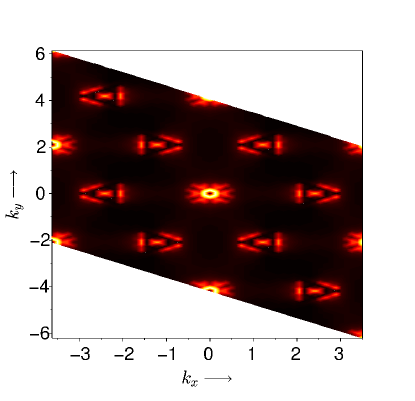
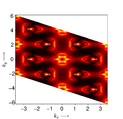

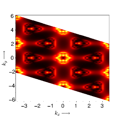
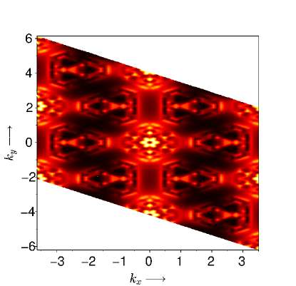

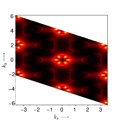
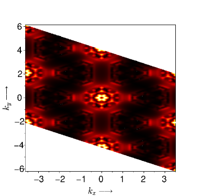

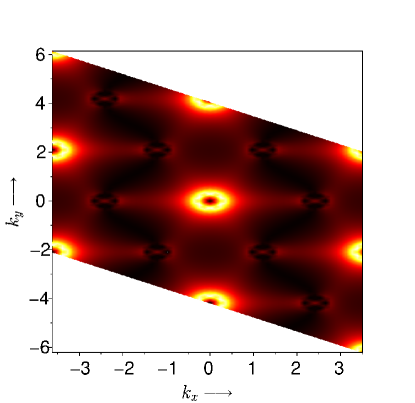
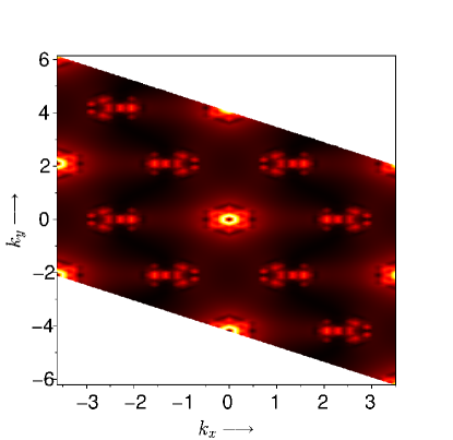

Since we are only interested in the change in the LDOS to first order in the impurity strength , we will take to be a small number and calculate . We first consider pristine graphene (i.e., in the absence of SO coupling and Zeeman field) when an impurity of strength is placed at the site of the unit cell centered at . The absolute value of the Fourier transform of is shown in Fig. 5 for different values of , with a lattice (i.e., ). Since the energy spectrum is found to have an exact or nearly exact six-fold degeneracy at most energies, we will calculate the LDOS by summing over the contributions from the six states with energy closest to the desired value of . Figure 5 shows that we get large and sharp peaks at the Dirac points, namely, the six points forming a hexagon around the center. [The six points are given by times , and , and times , and which are respectively equal to and up to reciprocal lattice vectors]. The peaks broaden as we move away from zero energy. (We note that the normalization of the LDOS calculated in this way is arbitrary to the extent that we have done the calculations for a particular system size and have not normalized the results to take that into account). We also note that the Fourier transform of is always zero at since that is just the difference in the number of states at that energy with and without the impurity, and we have chosen in such a way that the impurity does not change that number.
In Fig. 6, we show the absolute value of the Fourier transform of when an impurity of strength is placed at the site of the unit cell centered at , when there is a SOC of strength and a Zeeman field . Comparing Figs. 5 and 6, we find that the SOC and Zeeman field broaden the peaks at the Dirac points. This is expected since the SOC and Zeeman field open a gap and broaden the Dirac points in the dispersion shown in Fig. 1. Thus we find that the breadth of the LDOS peaks at the Dirac point is a measure of the strength of the SOC and/or Zeeman field in graphene.
Next, we study a distribution of non-interacting impurities instead of a single fixed impurity studied earlier. More specifically, we place impurities of strength on each of the six sites around a graphene hexagon, so that the integrated impurity strength is as before. We compute the absolute value of the Fourier transform of , as shown in Fig. 7, for and a Zeeman field . Comparing Figs. 6 and 7, we see that there no peaks at the Dirac points when the SOC is present. Further, the maximum value of the Fourier transform is now much smaller than in the case when the impurity is present only on a single site. These observations can be understood as follows. The Fourier transform of the two-point Green’s function in Eq. (LABEL:twopointg) is particularly large at the Dirac momenta and . Equation (15) shows that is composed of two such Green’s functions. Hence the Fourier transform of will be peaked at the difference of and , namely, at and (since ), provided that the Fourier transform of does not vanish at and . This is true if there is an impurity at a single site. However, if there are impurities of equal strengths at the six sites around a hexagon, the Fourier transform of this, given by , vanishes at and due to destructive interference between contribution from each point. Hence the Fourier transform of is negligible at and bena08 ; bena09 . Such a cancellation is unique for Dirac electrons in graphene and has been pointed out in the context of LDOS bena08 and STM spectra saha10 of a single impurity placed at the hexagon center in graphene; our work here points out that such a cancellation is qualitatively important for understanding the structure of LDOS for distributed impurities in graphene.
Finally, we study the LDOS in the presence of a magnetic impurity at a single site of graphene with SOC. Such an impurity provides a direct coupling to electron spin at that site. More specifically, we assume that the impurity is on the site of a unit cell located at and couples with strength to the -component of the spin:
| (16) |
For and a SOC of strength , the Fourier transform of the change in the LDOS is shown in Fig. 8 for two values of the energy . Comparing Figs. 6 and 8, we find that the scale of the change in the LDOS is much smaller for a magnetic impurity compared to a non-magnetic impurity of the same strength, namely, versus . This can be partly understood as follows. Since and anticommute, a unitary transformation of the Hamiltonian by leaves the SOC parameter unchanged but flips the impurity parameter . Since the LDOS must be invariant under this unitary transformation, it must be an even function of . To lowest order, therefore, the change in the LDOS must be of order for a magnetic impurity, while it is of order for a non-magnetic impurity. For , we therefore expect the change in the LDOS to be about 10 times smaller for a magnetic impurity. Thus we find that a magnetic impurity will have a smaller effect on LDOS compared to its non-magnetic counterpart.
IV Spin active graphene junctions
In this section we will study the differential conductance for either a junction of graphene with SOC and pristine graphene or two regions of pristine graphene which are separated from each other by finite width strips of various kinds, such as graphene with SOC or in an external Zeeman field. In Sec. IV.1, we carry out an analytical calculation for the differential conductance from a continuum theory. This will be followed by Sec. IV.2, where we will numerically calculate for finite-sized systems using a lattice model. A comparison between the results obtained by these two approaches is given in Sec. IV.3.
IV.1 Analytical calculation using continuum models

In this section, we analyze transport in graphene junctions with SOC. The geometry for such junctions which will be studied in this section is shown in Fig. 9. We begin with an analysis of the geometry in Fig. 9 (a) which represents a junction of pristine graphene and a part of graphene which has both Kane-Mele and Rashba SOC terms.
To analyze transport across such a junction, we first consider the system shown in Fig. 9 (a); the junction lies at . In region II where , the Hamiltonian is given by
| (17) | |||||
where the momentum is a conserved quantity having the same value everywhere. In the presence of the Rashba term, the energy-momentum dispersion is given by a quartic equation for ,
| (18) |
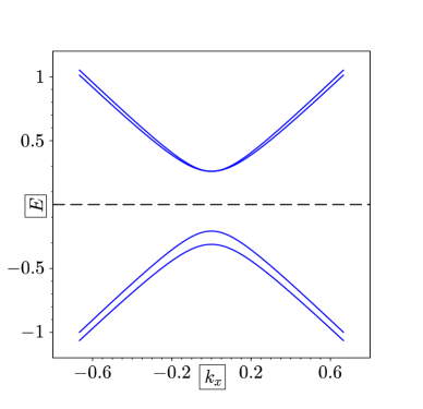
The solution of Eq. (18) leads to a gapped energy spectrum with four energy bands as shown in Fig. 10 for representative values , , , and . We observe that the spectrum is not symmetric about .
Given some values of and (which remain the same in the regions of pristine graphene and the strip region with SOC), the momentum in the strip can take four values given by
| (19) |
where the sign outside the square root is independent of the sign inside. We thus have four possible values of the momentum . Depending on the different parameters some of these values may be imaginary. If they are imaginary we will consider only the exponentially decaying solutions, while if they are real, we will choose the signs so that the group velocity is positive so that the electrons are moving right, i.e., towards . In any case, only two out of the four possible values of are physically allowed in region II; let us denote these two values by .
In what follows, we further use the fact that is a good quantum number. We will therefore only study the case . The case gives similar results since it is related to by the unitary transformation . The operator is not a good quantum number. However, we observe that . Since this transformation flips both and , it is enough to study the case of an incident electron with and all values of .
In region I of Fig. 9 (a), the Hamiltonian is given by Eq. (17) with . In this region, is also a good quantum number. The wave functions for right and left moving spin-up () and spin-down () electrons with momentum (where ) and energy are given by
| (24) | |||||
| (29) |
where . We now consider a spin-up electron which is incident on the junction with momentum and energy , where is the chemical potential or voltage applied in region I measured with respect to the Dirac point and is the Fermi energy. The reflected wave function can then be written as , where and are functions of and . Note that represents the amplitude for an incident spin-up electron to be reflected from the junction as a spin-down electron. It is therefore a direct measure of the spin active nature of the junction. Such a reflection process which converts a spin-up electron to a spin-down electron constitutes an analog in spin space of Andreev reflection from a superconductor in which an incident electron is converted to a reflected hole. The total wave function in region I can thus be written as
| (30) |
In region II, the presence of the Rashba term implies that is not a good quantum number. Consequently, the transmitted wave function will have amplitudes in both and sectors. For transmitted electrons with energy and momentum or , the wave functions can be found by solving the equation , where . Note that can be real or imaginary. A straightforward calculation yields
| (35) | |||||
| (36) | |||||
| (37) |
where is a normalization constant which ensures that . (The value of is not required in the expressions presented below). The transmitted wave function in region II is thus given by .
To find , and , we impose continuity of the wave function at the junction: . This leads to the following conditions on the various amplitudes:
| (38) |
The solution to these equations yields
| (39) | |||||
| (40) | |||||
Note that a non-zero value of is a consequence of the presence of two solutions, with , for a fixed energy and transverse momentum ; these two solutions merge when and the junction ceases to be spin active in this limit. We observe that for all values of if ; this shows that the specific voltage at which the spin-flip transport takes place can be controlled by the gap originating from the Kane-Mele term. ( also vanishes if the incident electron comes in at a glancing angle, namely, if so that ). For the incident electron, the range of values of goes from to , where , since we want to be equal to with real values of . Integrating over this range of , we find that the total incoming spin-up current and the reflected spin-down current are given by
| (41) |
We show plots of as a function of the applied voltage for a fixed in Fig. 11 (a), and as a function of for a fixed in Fig. 11 (b). These clearly demonstrate the spin active nature of the junction. We see that for a fixed , indeed vanishes at , but it eventually increases with . This demonstrates that the spin current can be electrically controlled.
Next, we analyze the geometry shown in Fig. 9 (b). In this geometry, pristine graphene resides in regions I and III, and graphene with Kane-Mele and Rashba SOC forms an interface region II of width which lies between those two regions. To analyze the transport in this system, we note that in regions I and III, is a good quantum number. In region I, the wave function is given by Eq. (30). Similarly, in region III, the transmitted wave function is given by
| (42) |
where denotes the probability for a spin- electron to be transmitted when the incident electron has .
In region II, the electron wave function is a linear superposition of electrons with momenta . The wave function of an electron with momentum is given by Eq. (36), while that for an electron with momentum is given by
| (47) | |||||
| (48) |
where is a normalization constant which ensures . Using Eqs. (36) and (48), the wave function in region II can be written as
| (49) |
The amplitudes , , , and can be found by matching the wave functions at and . This yields
| (50) | |||||
Using these we can compute the reflection and transmission probabilities and respectively, where can be or . Similarly, if the electron incident from region I had , we would have the reflection and transmission probabilities and . These must satisfy the unitarity relations
| (52) |
In what follows, we shall compute the tunneling conductance by solving Eqs. (50-LABEL:bcond3). and compute the transmission probabilities between two pristine graphene regions (region I and III) across a strip of graphene (region II) with a width , for and . In Figs. 12 (a) and (b), we show the transmission probabilities and versus for two values of the energy . Our plots clearly demonstrates a finite spin conversion as indicated by the dashed blue lines in Figs. 12(a) and (b). Given the transmission probabilities, the differential conductances can be calculated as follows. For a momentum , the current in the direction is given by . Let the chemical potentials in regions I and III in Fig. 9 (b) be and , so that the voltage bias between the two regions is given by . In the zero bias limit in which and , the differential conductance for an incident electron with spin being transmitted with spin ( can be or ) is given by
| (53) |
where is the width of the system in the direction (we assume that ). Integrating the -function over in Eq. (53) gives a denominator equal to which precisely cancels the appearing in the numerator of that equation. We thus obtain
| (54) |
where .
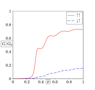
Instead of plotting versus , it is convenient to plot the ratio , where is the conductance when there is perfect transmission, i.e., . From Eq. (54) we find that in one particular valley. We then have the expressions
| (55) |
Fig. 12 (c) shows plots of and versus .
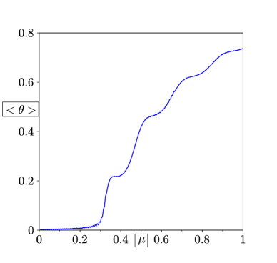
Another interesting quantity to consider is the rotation of the electron spin produced by region II. For each value of and , we know that a spin-up electron incident from region I converts to a linear superposition of spin-up and spin-down on being transmitted to region III, with amplitudes and respectively. In spin space, the linear superposition describes an electron whose spin polarization points at an angle with respect to the axis, where . We can therefore define an average rotation angle produced by region II as
| (56) |
where we have weighted the angle of rotation by the transmission probability . In Fig. 13 we show the average rotation angle as a function of for transmission across a strip of graphene with the same parameters as in Fig. 12. Fig. 13 clearly shows a finite spin rotation which increases as a function of in the zero-bias limit; this demonstrates the potential of these junctions as generators of electrically controllable spin current.
Before ending this section, we note that the calculations of this section serve as a proof of principle that a finite electrically controllable spin current may be generated in graphene junctions with finite SO coupling. There are many ways to enhance the magnitude of this current, which in our chosen parameter regime, appears to be rather small. For example, one can increase the bias voltage and/or the thickness of region II which will increase both and . Further, there may be other, more suitable geometries for larger spin current generation. In the next sub-section, we shall carry out numerical calculation from a lattice Hamiltonian which will address some of these issues and verify the approximate continuum calculation of the present section.
IV.2 Numerical calculation using lattice models
In this section, we provide a numerical analysis of the transport across the various junctions starting from a lattice model. The advantages of a lattice calculation over a continuum calculation are that a lattice calculation is straightforward to implement numerically (for instance, one does not have to impose any matching conditions on the wave functions), and one can easily study the effects of potentials or spin-orbit couplings which have arbitrary spatial profiles.
We will follow a procedure similar to the study of conductance across junctions of graphene and other materials sengupta06 ; bhattacharjee06 . We will assume that the strip is infinitely long in the direction, so that the momentum of an electron incident from one of the regions of pristine graphene is a good quantum number everywhere in the system. The incident energy is also a good quantum number. However, will vary from one region to another depending on the presence of SOC and a Zeeman field.
We will calculate the conductance numerically using a lattice model similar to the one shown in Fig. 2. We consider an electron incident from the pristine graphene at the bottom of that figure and we calculate the probabilities of reflection (back to the bottom) and transmission (to the pristine graphene at the top). An incident spin-up electron can get either transmitted or reflected as spin-up or spin-down; we will denote the corresponding probabilities by , , , and , respectively. Similarly an incident spin-down electron will have transmission and reflection probabilities given by , , , and .
The calculation is done as follows. Given the values of the momentum and energy (which we will henceforth assume to be positive), the dispersion for pristine graphene given in Eq. (I) uniquely fixes a momentum lying in the range . (It may happen that there is no real solution for ; this would imply that such a value of is not allowed for the given momentum . In that case we will set the transmission probabilities equal to zero). Then the incident and transmitted waves will have momentum while the reflected wave will have momentum . We now consider a single transmitted wave, with unit amplitude and equal to either or , which is located at the top of Fig. 2, and we find which superposition of the four possible incident and reflected waves at the bottom would give rise to such a transmitted wave (we have to allow for four possible waves in general since they could be either incident or reflected and they could have ). This superposition can be found by using Eqs. (7) to set up a matrix problem where the four reflection and incident amplitudes as well as the values of and inside the region with SOC or Zeeman field appear on the left side of an equation and the single transmitted wave at the top (with unit amplitude) appears as a source term on the right of the equation; the reflection and incident amplitudes are then found by doing a matrix inversion. Having found these amplitudes for the two cases where the transmitted wave has equal to and , we then invert these relations and find the reflection and transmission amplitudes when a wave is incident with unit amplitude . The modulus squared of the amplitudes give the reflection and transmitted probabilities as usual. Finally we check if the unitarity relations in Eq. (52) are satisfied.
Given the transmission probabilities, the differential conductances can be calculated as described in Sec. IV.1. We again arrive at Eqs. (53) and (54), except that the range of integration of in the lattice model is given by . However only those values of will contribute for which can be equal to with real values of . Once again, we will plot the ratio , where is the conductance when . Given a chemical potential lying between 0 and 1, we can show using Eq. (I) that
If is small, varies linearly with , namely, where is the Fermi velocity. This expression is exactly twice of what we expect for two species (due to the valleys) of massless Dirac electrons in the continuum. The additional factor of two is because we have considered the full range of from to ; this double counts the contribution from each of the two valleys since the transmission is invariant under . The double counting is not present in the ratio .
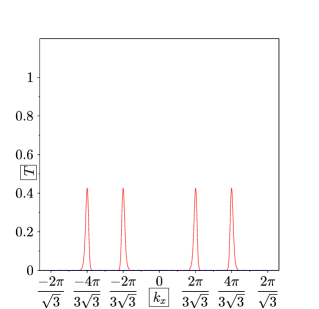
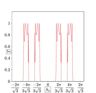
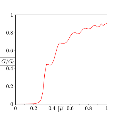
We now present our numerical results for a number of different cases. We first consider a strip of graphene with a width of 15 unit cells and a SOC of strength ; there is pristine graphene on both sides of the strip. (We take the Zeeman field to be zero). We will study the transmission probabilities as a function of the incident energy and the momentum . Since the SOC does not couple spin-up and spin-down electrons, we will have . Further, using the symmetries discussed after Eqs. (7), we can show that
| (58) |
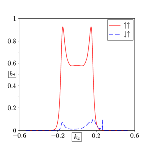
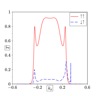
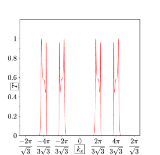
The second equation in (58) implies that it is sufficient to study . In Fig. 14, we show the transmission probability as a function of for three values of the energy, and . In each of the figures we see that there are regions of where is exactly zero or close to zero. These regions occur for two reasons. First, we have already seen that in pristine graphene, for a given value of , all possible values of are not allowed; for a disallowed value of , we set . Second, in graphene with a SOC of strength , the minimum value of energy occurs at the four values and and that minimum energy is given by . In Fig. 14 (a), the energy is only a little bit more than . Hence for all values of except the regions around the four special momenta, the energy of the incident electron lies inside the gap of graphene with SOC, and the wave function will decay exponentially inside that part of graphene. is therefore very small for all values of except near those four momenta.
In Fig. 14 we see some transmission resonances, namely, for certain values of and , we find that is close to 1. We can understand this as follows. If the energy does not lie in the gap of region of graphene with SOC, i.e., if the momentum in that region is real, then we expect a transmission resonance if is an integer multiple of . This is because such a condition implies that the wave function in the region with SOC will satisfy , where the sign depends on whether is an even or odd multiple of . Hence the wave function will match at and between pristine graphene and graphene with SOC, with the reflection amplitude being equal to zero at and the transmission amplitude being equal to at ; we will therefore get .
In Fig. 15, we show as a function of . We see that is very small for . As is increased to 1, also approaches 1 although some oscillations are visible. The locations of the maxima can be qualitatively understood as follows. We saw in the previous paragraph that there are transmission resonances if , where . Since Fig. 14 shows that the resonances are most prominent close to the Dirac points and , let us ignore the contributions from values of away from the Dirac points and approximate the dispersion inside graphene with SOC by ; this holds if is not too large. We therefore expect to show maxima when
| (59) |
The smallest values of give which are approximately the locations of the first three maxima in Fig. 15.
The system discussed above, with only a SOC present, enjoys an additional symmetry, namely,
| (60) |
In fact, even the transmission amplitudes are equal, . This can be shown as follows. We first note that for a particular value of equal to either or , Eqs. (7) have a symmetry resembling time reversal in which all numbers are complex conjugated. (This does not change the value of which simply appears as a parameter in those equations. This symmetry is therefore a bit different from the usual time reversal symmetry in which both and change sign). For a particular value of equal to or , this implies that the scattering matrix which relates the incoming waves at the top and bottom of the system to the outgoing waves must be symmetric, in addition to being unitary. (This can be proved as follows. If and denote the incoming amplitudes at the top and bottom, with plane wave factors and , and and denote the outgoing amplitudes at the top and bottom, with plane wave factors and , they must be related as . Complex conjugating this relation transforms to and vice versa. Time reversal symmetry then implies that we must have . This implies that , namely, is symmetric. Hence the transmission amplitude from the top to the bottom must be equal to the transmission amplitude from the bottom to the top. Next, we use the fact that the Hamiltonian in Eq. (6) (but without a magnetic field ) is symmetric under the parity transformation , , namely,
| (61) |
The transformation in Eq. (61) interchanges the and sublattices and also flips the component of the spin. This symmetry implies that the transmission amplitude from the top to the bottom for an electron with spin must be equal to the transmission amplitude from the bottom to the top for an electron with spin . Combining these two symmetries, we see that the transmission from the bottom to the top must be the same for .
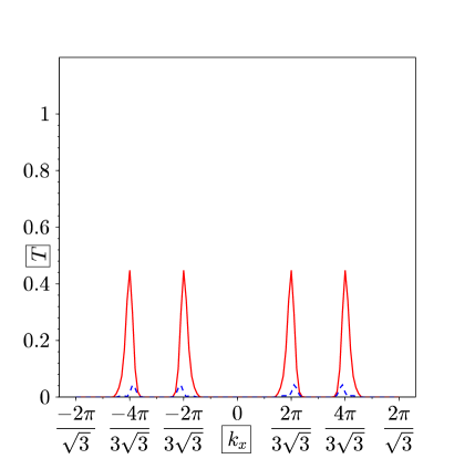
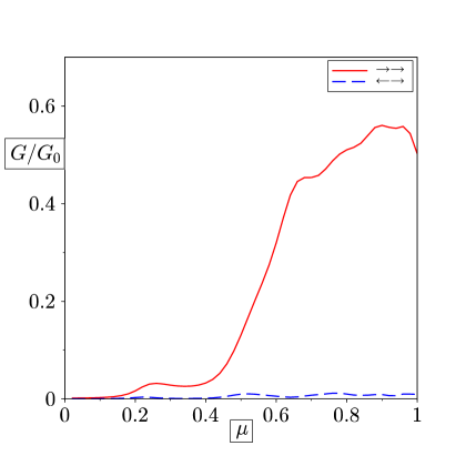
If the parity symmetry is broken, by applying a potential which depends on the coordinate in a way which is not invariant under reflection about the center of the region with SOC ( can be independent of both the spin and the sublattice index), we expect that the transmission amplitudes and will no longer be equal. Taking linear combinations of the incident electron so as to be quantized along, say, the direction, we find that the transmission amplitudes for a electron to be transmitted as a and electron are given by and respectively. (In fact these expressions hold for any component of the spin which is perpendicular to the axis, not just ). The latter will not be zero in general which implies that the component of the electron can flip when it transmits across a region with SOC and a parity-breaking potential. We demonstrate this effect in Figs. 16 and 17 for transmission across a strip of graphene with a width of 15 unit cells with a SOC of strength ; in addition, the bottom seven unit cells have a potential and the top eight unit cells have . Fig. 16 shows the probabilities for an incident electron with energy and to be transmitted into an electron with ; the transmission probabilities and are shown as functions of . (Here denote ). We see that there is a non-zero (though small) probability of conversion from to . Figure 17 shows plots of and versus for the same system. (The spin conversion effect discussed here is related to spin filter and spin valve effects which have been discussed in other papers, for instance, Refs. haugen08, ; yang13, ; song15, ).
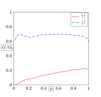
Next we consider a strip of graphene with a width of 15 unit cells and a Zeeman field in the direction with . (We take the SOC strength to be zero). To study this problem, we generalize Eqs. (7) to include a Zeeman field which couples spins and ; now , , , and will all be non-zero in general. We can then derive some symmetries similar to the ones discussed after Eqs. (7); using these we find that
| (62) |
where we define if and similarly for in the second equation. It is therefore enough to study and . (If , we also have the symmetry ).
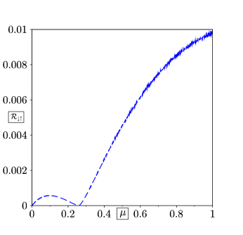
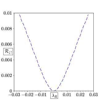
In Fig. 18, we show and as functions of . We see that is much larger than in the entire range of . This happens for this particular value of and can be qualitatively understood as follows. If electrons with (rather than ) were incident, they would be transmitted with unit magnitude but with a phase difference. If the electrons have energy , the dispersion inside graphene with a Zeeman field would be given by , if is not too large. (For simplicity, we are assuming that is equal to one of the Dirac points or ). Here denote the values of the component of the momentum for . The phase difference between the electrons with is given by . For and , the phase difference is which is close to . Hence electrons with are perfectly transmitted but with almost opposite signs. Hence incident electrons with , which is given by the linear combination will be transmitted almost as the linear combination which is the same as . We thus see an almost perfect conversion of spin from to . Note that this approximate argument is independent of the energy which explains why is much larger than for all in Fig. 18.
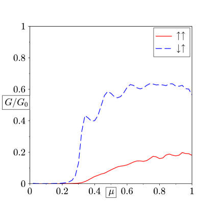
Finally we consider a strip of graphene with a width of 15 unit cells and a SOC of strength , followed immediately by another strip with the same width of 15 unit cells where there is a Zeeman field but no SOC; there is pristine graphene on both sides of the two strips. We consider an incident electron which first strikes the region with SOC and we study the transmission after it leaves the region with a Zeeman field. Once again , , , and will all be non-zero in general, and the symmetries in Eqs. (62) will hold. In Fig. 19, we show and as functions of .
IV.3 Discussion of spin active junctions
To summarize and compare the results presented in Secs. IV.1 and IV.2, we have discussed two kinds of junctions which are spin active, i.e., they can rotate the direction of spin of an electron which is incident on the junction. The first example, discussed in Sec. IV.1, is a region of graphene which has a combination of Kane-Mele and Rashba SOC. The Rashba SOC does not conserve the spin; hence it is not unexpected that it can give rise to a spin active junction of spin-orbit coupled and pristine graphene. We have used a continuum theory (valid near the and points) to analytically calculate the reflection probability from a junction of spin-orbit coupled and pristine graphene and the transmission probability and differential conductance (obtained by integrating the transmission over all incident momenta) through a strip of spin-orbit coupled graphene. To quantify the spin active nature, we have studied the amount of spin rotation as a function of the applied voltage and the strength of the Rashba SOC. In the second example, discussed in Sec. IV.2, we studied the effect of a strip of graphene with Kane-Mele SOC, a Zeeman field (in a direction perpendicular to the SOC so that the two terms do not commute), and a potential which is not parity symmetric. Since the calculation cannot be analytically done for a general non-parity symmetric potential, we have used the tight-binding model to numerically calculate the transmission probability and difference conductance across such junctions. Once again we find that the junction is generally spin active.
Comparing the results for the different junctions, we see that a Zeeman field which is perpendicular to the Kane-Mele SOC and a Rashba SOC are most effective in producing spin active junctions. A non-parity symmetric potential along with a Kane-Mele SOC is relatively less effective.
V Discussion
In this work, we have studied edge states, effects of impurities, and spin active junctions in spin-orbit coupled graphene along with the presence/absence of a Zeeman term which originates from proximity of the graphene sheet to a suitably chosen ferromagnetic film. The SOC, which may arise due to proximity of graphene to topological insulator films, has been taken to be of either Kane-Mele or Rashba form.
Our study concentrates on three properties of such graphene systems. First, we have shown that a junction between graphene with the Kane-Mele type of SOC and pristine gapless graphene (with no SOC) supports robust chiral edge states provided that the edge separating the two regions is of the zigzag type; no such states exist for the armchair edges. We have also shown that these edge states are robust in spite of the presence of gapless pristine graphene on one side of the junction; this robustness arises due to the fact that the decay length of these states vanishes for . We have pointed out that such behavior is in complete contrast to the behavior of conventional edge modes where the decay length diverges in the limit of vanishing gap.
Second, we have studied the change in the LDOS originating from either a single or a specific distribution of impurity atoms in spin-orbit coupled graphene. We have shown that for a single impurity the Fourier transform of the LDOS displays peaks near the Dirac points with a finite width; the width of these peaks is a direct measure of the strength of the induced spin-orbit interaction. We have also shown that for a specific distribution of impurity atoms (distributed at the corners of a graphene hexagon), the Fourier transform of LDOS exhibits an absence of peaks near the Dirac points. Such an absence can be traced back to the destructive interference of the contribution to the LDOS from each of the impurity sites and is a direct signature of the Dirac nature of graphene electrons. Such an effect has been discussed earlier in the context of LDOS bena08 and STM spectra of single impurity placed at the center of a hexagon in graphene saha10 ; however, its manifestation has not been pointed out for a distribution of impurities to the best of our knowledge.
Although we have only discussed the effects of a single impurity or a small number of impurities in this paper, our results can also be used to understand what would happen if there was a finite density of impurities which are far from each other, so that the scattering from the different impurities is incoherent. The Fourier transform of the change in the LDOS would then be given by the Fourier transform of the LDOS for a single impurity multiplied by the density of impurities. Hence the Fourier transform of the LDOS of a finite density of impurities will share the features of the Fourier transform of the LDOS of a single impurity such as the peaks at the Dirac points. The Fourier transform of the LDOS for a finite density of impurities can be measured by a light scattering experiment.
Third, we have studied junctions of spin-orbit coupled graphene (with both Kane-Mele and Rashba terms) and pristine graphene. We have shown that such junctions are generally spin active and that they may be used to generate electrically controllable spin currents in graphene. We have demonstrated this in a variety of junctions with analytic computations using low-energy effective Dirac-like Hamiltonians and with numerical calculations based on microscopic lattice models. We have also discussed several ways of enhancing the spin current and pointed out the role of Zeeman coupling terms and parity-symmetry breaking potential terms in this context.
The experimental verification of our work would involve preparation of graphene samples with strong SOC. Since the intrinsic SOC in graphene is extremely weak, this needs to be done using a proximate material with strong SOC; the hybrid samples of topological insulators atop a graphene sheet which have already been experimentally studied are ideal for this purpose. The LDOS for impurities in such samples can be measured using an STM; the Fourier transform of the LDOS can then be computed schouteden . The prediction of our present work is that the width of the peak of the Fourier transform of this LDOS would be a direct measure of the strength of the induced SOC. To form junctions of spin-orbit coupled graphene with its pristine counterpart, we need to deposit the topological insulator over a part of the graphene sample leaving the rest of the sample in its pristine form. We predict that if such a junction has a zigzag edge separating the spin-orbit coupled and pristine graphene, there would be additional chiral edge states whose density of states could be measured by STM; no such edge states would exist if an armchair edge separates the two regions. Finally, for spin active junctions we suggest measurement of the spin current via standard tunneling conductance measurements where the injection and detection of current is done with spin-polarized leads of opposite polarities. This will serve as a direct measure of .
To conclude, we have studied edge states, effects of impurities, and spin active junctions in graphene which has spin-orbit coupling. Our results points out the presence of robust chiral edge states in graphene junctions separating spin-orbit coupled graphene from its pristine counterpart with novel properties of their decay length, shows that the local density of states originating from impurities in spin-orbit coupled graphene near the Dirac points can serve as a measure of the strength of the induced spin-orbit coupling for graphene, and demonstrates that junctions of spin-orbit coupled and pristine graphene are spin active and may be used to generate electrically controllable neutral spin currents. We have proposed realistic experiments which may test our theory.
Acknowledgements.
We thank Arindam Ghosh, Kimberly Hsieh and Abhiram Soori for discussions. D.S. thanks DST, India for support under Grant No. SR/S2/JCB-44/2010.References
- (1)
- (2) C. W. J. Beenakker, Rev. Mod. Phys. 80, 1337 (2008).
- (3) A. H. Castro Neto, F. Guinea, N. M. R. Peres, K. S. Novoselov, and A. K. Geim, Rev. Mod. Phys. 81, 109 (2009).
- (4) S. Das Sarma, S. Adam, E. H. Hwang, and E. Rossi, Rev. Mod. Phys. 83, 407 (2011).
- (5) M. O. Goerbig, Rev. Mod. Phys. 83, 1193 (2011).
- (6) D. N. Basov, M. M. Fogler, A. Lanzara, F. Wang, and Y. Zhang, Rev. Mod. Phys. 86, 959 (2014).
- (7) M. I. Katsnelson, K. S. Novoselov, and A. K. Geim, Nature Phys. 2, 620 (2006).
- (8) V. Lukose, R. Shankar, and G. Baskaran, Phys. Rev. Lett. 98, 116802 (2007).
- (9) C. W. J. Beenakker, Phys. Rev. Lett. 97, 067007 (2006).
- (10) S. Bhattacharjee and K. Sengupta, Phys. Rev. Lett. 97, 217001 (2006); S. Bhattacharjee, M. Maiti, and K. Sengupta, Phys. Rev. B 76, 184514 (2007).
- (11) M. Titov and C. W. J. Beenakker, Phys. Rev. B 74, 041401(R) (2006).
- (12) M. Maiti and K. Sengupta, Phys. Rev. B 76, 054513 (2007).
- (13) K. Sengupta and G. Baskaran, Phys. Rev. B 77, 045417 (2008).
- (14) M. Hentschel and F. Guinea, Phys. Rev. B 76, 115407 (2007).
- (15) T. O. Wehling, A. V. Balatsky, M. I. Katsnelson, A. I. Lichtenstein, and A. Rosch, Phys. Rev. B 81, 115427 (2010).
- (16) J.-H. Chen, L. Li, W. G. Cullen, E. D. Williams, and M. S. Fuhrer, Nature Phys. 7, 535 (2011).
- (17) B. Uchoa, T. G. Rappoport, and A. H. Castro Neto, Phys. Rev. Lett. 106, 016801 (2011).
- (18) V. V. Cheianov and V. I. Fal’ko, Phys. Rev. Lett. 97, 226801 (2006).
- (19) E. Mariani, L. I. Glazman, A. Kamenev, and F. von Oppen, Phys. Rev. B 76, 165402 (2007).
- (20) C. Bena, Phys. Rev. Lett. 100, 076601 (2008).
- (21) C. Bena, Phys. Rev. B 79, 125427 (2009).
- (22) A. V. Shytov, M. I. Katsnelson, and L. S. Levitov, Phys. Rev. Lett. 99, 246802 (2007).
- (23) M. Z. Hasan and C. L. Kane, Rev. Mod. Phys. 82, 3045 (2010).
- (24) X.-L. Qi and S.-C. Zhang, Rev. Mod. Phys. 83, 1057 (2011).
- (25) C. L. Kane and E. J. Mele, Phys. Rev. Lett. 95, 226801 (2005).
- (26) L. Kou, B. Yan, F. Hu, S.-C. Wu, T. O. Wehling, C. Felser, C. Chen, and T. Frauenheim, Nano Letters 13, 6251 (2013).
- (27) J. Zhang, C. Triola, and E. Rossi, Phys. Rev. Lett. 112, 096802 (2014).
- (28) K. Zollner, T. Frank, S. Irmer, M. Gmitra, D. Kochan, and J. Fabian, arXiv:1507.02820.
- (29) C. Dutreix, M. Guigou, D. Chevallier, and C. Bena, Eur. Phys. J. B 87, 296 (2014).
- (30) H. Haugen, D. Huertas-Hernando, and A. Brataas, Phys. Rev. B 77, 115406 (2008).
- (31) H. X. Yang, A. Hallal, D. Terrade, X. Waintal, S. Roche, and M. Chshiev, Phys. Rev. Lett. 110, 046603 (2013).
- (32) Y. Song and G. Dai, App. Phys. Lett. 106, 223104 (2015).
- (33) S. Rachel and M. Ezawa, Phys. Rev. B 89, 195303 (2014).
- (34) C.-C. Liu, H. Jiang, and Y. Yao, Phys. Rev. B 84, 195430 (2011).
- (35) K. Nakada, M. Fujita, G. Dresselhaus, and M. S. Dresselhaus, Phys. Rev. B 54, 17954 (1996).
- (36) M. Kohmoto and Y. Hasegawa, Phys. Rev. B 76, 205402 (2007).
- (37) J. L. Lado, N. Garcia-Martinez, and J. Fernandez-Rossier, Synth. Met. 210, 56 (2015).
- (38) K. Sengupta, R. Roy, and M. Maiti, Phys. Rev. B 74, 094505 (2006).
- (39) Y. Jiang, F. Lu, F. Zhai, T. Low, and J. Hu, Phys. Rev. B 84, 205324 (2011).
- (40) K. Saha, I. Paul, and K. Sengupta, Phys. Rev. B 81, 165446 (2010).
- (41) K. Schouteden, P. Lievens, and C. Van Haesendonck, Phys. Rev. B 79, 195409 (2009).