Design principles for shift current photovoltaics
Abstract
While the basic principles of conventional solar cells are well understood, little attention has gone toward maximizing the efficiency of photovoltaic devices based on shift currents. By analyzing effective models, here we outline simple design principles for the optimization of shift currents for frequencies near the band gap. Our method allows us to express the band edge shift current in terms of a few model parameters and to show it depends explicitly on wavefunctions in addition to standard band structure. We use our approach to identify two classes of shift current photovoltaics, ferroelectric polymer films and single-layer orthorhombic monochalcogenides such as GeS, which display the largest band edge responsivities reported so far. Moreover, exploring the parameter space of the tight binding models that describe them we find photoresponsivities that can exceed 100 mA W-1. Our results illustrate the great potential of shift current photovoltaics to compete with conventional solar cells.
Introduction - Cost-effective, high-performing solar cell technology is an essential piece of a sustainable energy strategy. Exploring approaches to photo-current generation beyond conventional solar cells based on pn junctions is worthwhile given that their performance is in practice constrained by the Shockley-Queisser limitShockley and Queisser (1961). One of the most promising alternative sources of photocurrent is the bulk photovoltaic effect (BPVE) or ‘shift current’ effect, a non-linear optical response that yields net photocurrent in materials with net polarization Kraut and von Baltz (1979); Belinicher and Sturman (1980); von Baltz and Kraut (1981); Presting and Von Baltz (1982); Sturman and Sturman (1992); Aversa and Sipe (1995); Kristoffel et al. (1982); Sipe and Shkrebtii (2000); Král et al. (2000): Contrary to conventional pn junctions, the BPVE is able to generate an above band-gap photovoltage Ji et al. (2010), potentially allowing the performance of BPVE-based photovoltaics to surpass conventional ones. However, closed-circuit currents generated via the BPVE reported in the literature have typically been small compared to those generated in pn junction photovoltaicsZheng et al. (2015); Young and Rappe (2012); Brehm et al. (2014). Recent interest in the BPVE also stems from the proposal that it may be at work in a promising class of materials for photovoltaics known as hybrid perovskites Zheng et al. (2015), an extremely active field of research Hodes (2013); Egger et al. (2015); McGehee (2014); Antonietta Loi and Hummelen (2013); Even et al. (2013); Stroppa et al. (2014); Zhang et al. (2015a); Saba et al. (2014); Leguy et al. (2015); Motta et al. (2015); Filip et al. (2014); Saidaminov et al. (2015); Eames et al. (2015); Heo et al. (2013).
The fundamental requirement for a material to produce a current via the BPVE is that it breaks inversion symmetry, allowing an asymmetric photoexcitation of carriers. But despite considerable case-by-case study of the BPVE, the necessary ingredients to optimize a BPVE-based solar cell are not sufficiently well understood. As with conventional solar cells, band gaps in the visible (1.1-3.1 eV) Young et al. (2012); Brehm et al. (2014) and large electronic densities of states Young and Rappe (2012); Wang et al. (2015) are always beneficial. In addition, to produce a solar cell that responds to unpolarized sunlight, a highly anisotropic material must be used, since otherwise there is no preferred direction for the current to flow. But beyond these natural requirements, our only guiding knowledge is that the shift current depends explicitly on the nature of the electronic wavefunctions Wang and Rappe (2015); Wang et al. (2015) and that it is not correlated with the material polarization in any obvious way Brehm et al. (2014) despite the fact that both shift currents and polarization originate from inversion symmetry breaking.
In the current situation, a more generic understanding of what makes the BPVE strong is highly desirable. When tackling complex material science problems, stripping off all complications and optimizing the simplest model that captures the relevant physics often proves the best strategy, as shown for example in thermoelectricity studies Mahan and Sofo (1996); DiSalvo (1999); Murphy et al. (2008). In this work, we present simple design principles for BPVE optimization based on the study of an effective model for the band edges. With this model, the band edge shift current is given by the product of the joint density of states (JDOS) and a matrix element, both given by simple expressions in terms of a few model parameters. The simplicity of the model allows us to derive the main principle that band edges with semi-Dirac type of Hamiltonians are the best starting point to obtain large band edge prefactors. In addition, by relating the effective model parameters to realistic tight-binding models, we can predict that several materials with the required band structure have larger shift currents than any reported so far.
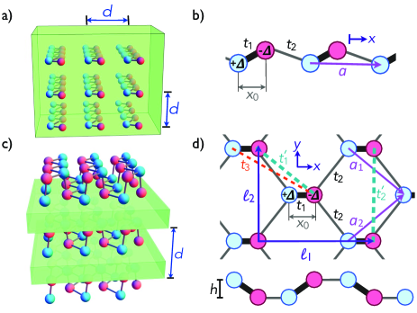
Results - In our search for materials we should look for large JDOS in systems where the band edge is closely aligned with the peak of the solar spectrum, around 1.5 eV. Since the band edge always induces a Van Hove singularity in the density of states, the requirement of a large peak in the photoresponse can be naturally better satisfied by low-dimensional materials, which generically present stronger singularities Van Hove (1953). Materials of one and two dimensions are therefore the focus of this work. Among one-dimensional materials, ferroelectric polymers are suitable candidates for shift-current photovoltaics: they strongly break inversion symmetry, some have suitable band gaps for photovoltaics applicationsNalwa (1995); Lovinger (1983); Gontia et al. (1999); Rice and Mele (1982), and they can be produced in macroscopically oriented samples. For these reasons, we consider solar cells consisting of such polymer films, shown in Fig. 1(a). Two-dimensional materials Geim and Grigorieva (2013) also have great potential for photovoltaics, as shown by demonstration of a pn-junction photovoltaic effect in dichalcogenide heterostructures Britnell et al. (2013); Yu et al. (2013); Bernardi et al. (2013), and in few-layer black phosphorus Buscema et al. (2014). However, these well known 2D semiconductors have vanishing shift currents because of either inversion or rotation symmetry. Group IV monochalcogenides have emerged in the past years as a new familiy of inversion-breaking, anisotropic 2D materials with fascinating properties Singh and Hennig (2014); Gomes and Carvalho (2015); Antunez et al. (2011); Li et al. (2016); Rodin et al. (2016), and interest is growing as thin films of all four members of the family, GeSLi et al. (2012); Ulaganathan et al. (2016); Vaughn II et al. (2010); Ramasamy et al. (2016), GeSeVaughn II et al. (2010); Ramasamy et al. (2016), SnSBrent et al. (2015); Xia et al. (2016) and SnSeLi et al. (2013); Zhang et al. (2015b); Zhao et al. (2015), have now been isolated experimentally. In this work, we show that GeS is ideally suited to realize high values of the BPVE. Their GeS structure is shown in Fig.1(c).
To understand how to optimize the photoresponse, we first discuss how the shift current can be computed for a tight binding model, and then we proceed to apply this formalism to describe a generic band edge and the response of particular materials.
Shift current - In this work we consider the shift current contribution to the BPVE and we shall use both terms interchangeably (note the BPVE can have other contributions as wellSturman and Sturman (1992)). With electric field at frequency and linearly-polarized in the direction, the shift current is a DC response of the form Sturman and Sturman (1992)
| (1) |
Defining an intensity for each polarization, , we define the photoresponsivity as the current density generated per incident intensity , which gives . Note that in conventional solar cells the current is also linear with intensity. For a D-dimensional system, takes the form Aversa and Sipe (1995); Sipe and Shkrebtii (2000)
| (2) |
where , with the speed of light, the vacuum permittivity, and accounts for the spin degeneracy. In what follows we set . Summation of indices is explicitly indicated using the summation symbol. The sum is over all Bloch bands, with the energy difference between bands and and the difference of Fermi occupations, which we take at zero temperature. The integrand is
| (3) |
where are the inter-band matrix elements of the position operator (or inter-band Berry connections), defined as for and zero otherwise, where is the eigenstate of band . A semicolon denotes a generalized derivative , where is the diagonal Berry connection for band .
.
Generic two band model - With the aim of describing the shift current response of the band edge of a semiconductor, next we consider the shift current of a generic two band model. The Fourier transform of the real space Hamiltonian is performed with the choice of phases , where is a localized orbital and is the position of site in the unit cell. This choice is made in order to naturally incorporate the action of the position operator, see Refs. Bena and Montambaux (2009); Dobardić et al. (2015); Fruchart et al. (2014). The Hamiltonian matrix takes the form
| (4) |
where is the identity matrix, are the Pauli matrices and and are generic functions of momenta (the momentum label is omitted to simplify notation). The conduction and valence bands are given by , , respectively and . Note that this basis choice implies that the Hamiltonian matrix elements are not periodic in the Brillouin Zone, with a reciprocal lattice vector.
To compute the shift current, the direct use of Eq. 3 requires the evaluation of derivatives of Bloch functions, which can be difficult to compute numerically. Previous works von Baltz and Kraut (1981); Aversa and Sipe (1995); Sipe and Shkrebtii (2000) have addressed this problem with the use of identities that replace wavefunction derivatives with sums over all states of matrix elements of Hamiltonian derivatives. These identities are known as sum rules and rely on the fact that momentum and velocity operators are proportional in the plane wave basis , which is not true in the tight binding formalism. In this work we derived a generalized sum rule appropriate for tight binding models (see Methods section), from which the integrand Eq. 3 can be evaluated for any two-band model in terms of the Hamiltonian derivatives only. The result is
| (5) |
where the compact derivative notation and is used. Eq. 5 is one of the main results of this work. Several general principles to maximize the band edge shift current can be derived from this expression. A straightforward one is that, since this expression does not depend on , particle-hole asymetry does not influence the shift current at all. Therefore is set to zero from now on. The additional term that appears only for tight binding models in this more general sum rule is , which is absent in previous formulations. For a direct band gap, this term dominates the response exactly at the band edge, since to lowest order in the first term always has constant contribution, while the second one is at least linear in for any model due to the energy derivative . For this term to be finite, the three Pauli matrices in the Hamiltonian must have constant, linear, and quadratic coefficients, in any order. Satisfying this low-energy constraint can be taken as another general principle in the search for materials with large shift current.
More explicit guidelines can be obtained by considering an explicit low-energy model with a direct band gap at a time reversal invariant momentum. Expanding the Hamiltonian around it we get
| (6) |
Time reversal symmetry prevents quadratic terms in , and we have taken the linear term to be in the direction without loss of generality. Note this type of linear term requires the breaking of any rotation symmetry with . The band gap of this model is . Evaluating 5 we get
| (7) | ||||
| (8) |
while . Also note that in order to have a non-zero shift current quadratic terms in or are required. In 2D, the fact that is in general non-zero means that the current need not be in the direction of the electric field polarization.
The shift current close to the band edge can now be obtained by substituting Eqs. 7-8 into Eq. 2, which gives
| (9) |
where is the JDOS. Eq. 9 provides an analytical formula for close to the band edge for a very general class of models. This simple expression allows one to disentangle the contributions of the shift current integrand and the JDOS and hence to optimize them independently.
To maximize the response we therefore require band structures where the JDOS has a strong singularity. It is well known that in the 1D case, the generic JDOS diverges as a square root, . 1D systems such as polymers or nanowires or systems in the quasi 1D limit will in general have a large response. In 2D, the band edge JDOS has a finite jump of , where are the average effective masses for valence and conduction bands. A singular thus occurs in 2D when the inverse effective mass vanishes. In the effective model in Eq. 6, this happens when , which realizes what we may call a gapped semi-Dirac dispersion Banerjee et al. (2009), since the coefficients of and are linear and quadratic in momentum, respectively. In such a case we have (full expressions for may be found in the Methods section).
For materials with large JDOS, the current can be further enhanced by appropriately tuning the parameters in Eqs. 7-8. This is most easily discussed if these parameters can be related to microscopic lattice models. In the next section, we discuss tight-binding models for simple materials that realize the described types of band structures.
Material realizations and lattice models - As a realization of the 1D case, we consider ferroelectric polymers that break inversion symmetry such as polyvinylidene fluoride or disubstituted polyacetileneSu et al. (1979); Rice and Mele (1982); Gontia et al. (1999). This system is described by the tight-binding model schematically shown in Fig. 1(b), defined in terms of two types of hoppings, and , alternating on-site potentials , and orbital centers at and . With our choice of basis functions, the Hamiltonian is specified by and , where is the lattice constant and the distance between closest neighbors is Su et al. (1979) . For estimates of the tight binding parameters, we consider the example of disubstituted polyacetilene that was experimentally realized in Ref. Gontia et al., 1999, with a band gap of 2.5 eV. For regular polyacetilene, where , the hopping parameters and band gap have been estimated as Su et al. (1979) eV, eV, eV. Assuming the same hopping for the disubstituted version, we use eV to match the observed band gap. Note that the dispersion does not depend on .
Using Eq. 2 and Eq. 5 we can now compute the shift current for this 1D model. Expanding about the low energy momentum and performing a constant rotation of the Pauli matrices, we obtain an effective model as Eq. 6 with parameters and , , .
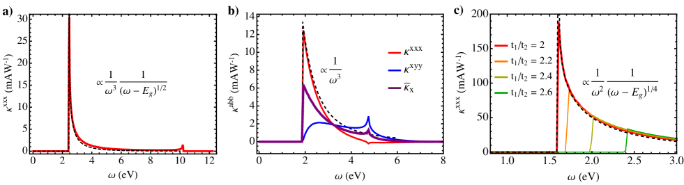
To be able to compare the responsivity of these materials to that of a 3D system, we consider a stack of polymers as depicted in Fig. 1(a), separated by a distance which we take to be equal to the lattice constant of the polymer . The photoresponsivity is then . The typical photoresponsivity spectrum of this model with this convention is shown in Fig. 2(a).
For the 2D case, we require a layered material that breaks both inversion and rotational symmetries. The most popular of the recently isolated 2D semiconductors break either inversion (BN, MoS2) or rotational symmetries (black phosphorus Xia et al. (2014), Re Liu et al. (2015)), but not both. An inversion symmetry breaking version of the strongly anisotropic black phosphorus, a group V element, can be obtained combining elements of the IV and VI groups. These group IV monochalcogenides, such as GeS, are predicted to be stable in the monolayer form with the orthorhombic structure of black phosphorus Singh and Hennig (2014); Gomes and Carvalho (2015).
These materials can be described with a tight binding model similar to the one used for black phosphorusRudenko and Katsnelson (2014); Rudenko et al. (2015); Ezawa (2014). While the GeS unit cell contains two Ge-S pairs at different heights, a unit cell with a single Ge-S pair can be used when the physics to be probed is insensitive to the heights of the atoms (see Methods for a detailed explanation). The two band Hamiltonian is specified by , where and , and . and are the lattice vectors. See Fig. 1(d) for the definition of the hopping integrals. Again note the dispersion is independent of . The specific values of the tight-binding parameters for GeS have been obtained by fitting an ab-initio calculation as described in the Methods section, where the coefficients of the low energy model near the band edge are also shown. Note in this lattice structure there is a mirror symmetry , which is represented as the identity, and restricts . (This is so because both conduction and valence bands are even under the symmetry, as it also happens in black phosphorus. This is also the result of our ab-initio calculation.) This symmetry still allows a linear term of the form , crucial for the semi-Dirac type of band structure. In this model, the semi-Dirac limit is realized when Montambaux et al. (2009).
We consider a stack of monolayers separated by , as shown in Fig. 1(c). In this case, we consider an inert spacer layer between the GeS layers to avoid the restoration of inversion symmetry that would occur if we were to stack GeS into its natural bulk form. The 3D photoresponsivity of this model, given by , is computed using Eqs. 2 and 5. To make contact with the 1D case we consider a stacking distance and . The results are shown in Fig. 2(b). We see that both and are in general finite, and the polarization average is also finite due to the strong anisotropy.
The response of the monochalcogenides is large because they are close in parameter space to the gapped semi-Dirac Hamiltonian. This is best illustrated by considering the evolution of a fictitious system where the hoppings are tuned (with for simplicity) to the semi-Dirac case , where the divergence of the response is clearly appreciated. This evolution is shown in Fig. 2(c).
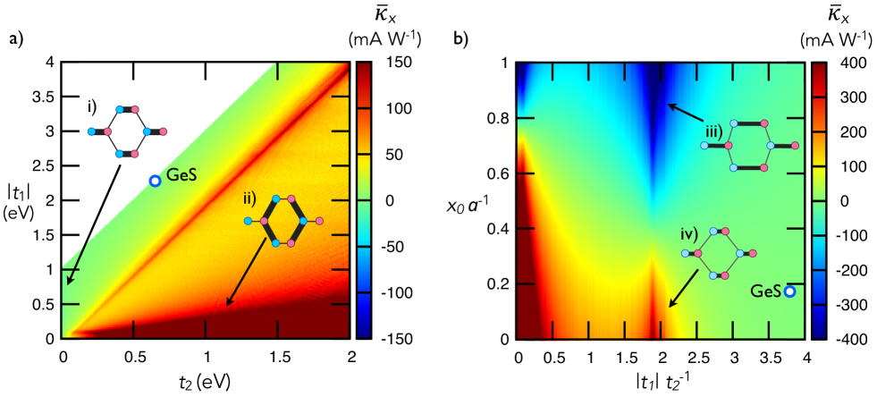
Further optimization - After describing the representative tight-binding models with large JDOS, we may now address a more systematic analysis of the photoresponsivity. First, we consider exploring the phase diagram of the monochalcogenides by sweeping in parameter space while the band gap is fixed at 1.89 eV by choosing appropriately and for simplicity. Fig. 3(a) shows the polarization averaged photoresponsivity, , for the parameters and . This phase diagram summarizes nicely the most physically relevant regimes where the shift current is large due to a divergent JDOS, namely the 1D dimensional limit where , and the semi-Dirac regime where . In this phase diagram, the point corresponding to and of GeS is shown as a white circle with blue outline.
Next we illustrate a very important feature of the behavior of the shift current integrand. Eqs. 7-8 depend generically on the hoppings and lattice parameters. The energy does not depend on the parameter , but the wavefunctions do. In Fig. 3(b), we show the peak photoresponsivity as a function of and . A large response is observed in the semi-Dirac limit . However, a very strong dependence on and even a sign change is also observed. The dependence on dramatically illustrates the fact that the shift current depends not only on the band structure, but also on the wavefunctions. This can be seen explicitly in the fact that the effective mass is independent of , but the combination appearing in the shift current integrand is not. In particular vanishes for , which means that regardless of the JDOS, the band edge response can actually be zero. This behavior is characteristic of Berry connections, which depend explicitly on the positions of the sites in the unit cell.
Discussion - In this work, we have shown how an effective model for the band edge enables a clean separation of the two factors that contribute to a large shift current: the standard JDOS and the shift current matrix element. This model also allows us to readily identify materials with semi-Dirac-like Hamiltonians as those where both factors can be made large. Several other general conclusions can be drawn from the form of the effective shift current integrand in Eqs. 7-8. First, since the factor becomes at the band edge, materials with smaller gaps are expected to have larger shift currents. A second conclusion is that while looking for materials with large JDOS is a good guiding principle, the shift current integrand depends on other microscopic details that can change the response dramatically. Within our simple model, the shift current can be maximized by bringing the two sites of the unit cell closer together, which is a requirement that the monochalcogenides satisfy well. Materials that may perform even better than GeS may be searched for exploring different chemical compositions, alloying, or by strain engineering.
Our results were made possible by the derivation of a new sum rule appropriate for tight-binding models. With this sum rule, our work can be easily extended to tight-binding models with more than two bands, or systems where the minimum direct gap is not at a time-reversal invariant momentum. We expect that the formalism developed here will provide the necessary link to combine ab-initio methods with effective models, allowing for more in-depth, systematic study of shift current photovoltaics.
Our results should be compared to known ferroelectric materials that have been recently studied. In the visible range of frequencies, eV, we find peak values of 0.1 mAW-1 in BiFeO3 Young et al. (2012), 1 mAW-1 in hybrid perovskites Zheng et al. (2015) and a maximum 10 mAW-1 in BaTiO3Young and Rappe (2012) or NaAsSe2 Brehm et al. (2014). The realistic materials that we propose present larger responsivities, with the additional advantage that the peak is by construction at the band edge. Moreover, as Fig. Fig. 2(c) and Fig. 3(b) show, peak responses on the order of several hundreds of mAW-1 could be achieved with materials closer to the semi-Dirac regime. To compare with conventional photovoltaic mechanisms, the total current per intensity of a crystalline Si solar cell exposed to sunlight is about 400 mAW-1 Pagliaro et al. (2008).
Given these numbers, our work is a sign that shift current photovoltaics capable of surpassing conventional solar cells may be close at hand, and a push to investigate their full potential using methods discussed in this work – along with established techniques – is warranted. We believe that the simple principles derived in our work will serve as a guide for both theory and experiment in the development and optimization of the next generation of shift current photovoltaics.
Methods
Shift current - To make contact with previous work, we note the shift current integrand in Eq. 3 is sometimes expressed in terms of the phase of the inter-band matrix element as where
| (10) |
is known as the shift vector. The response to a natural light source such as sunlight, which is unpolarized, is obtained by averaging over polarization. Taking we have
| (11) |
Sum rule - The expression for the shift current presented in the main text can be obtained by the use of a sum rule for the quantity , which is obtained from the identity
| (12) |
Evaluating both sides explicitly for , the identity can be expressed as
| (13) | ||||
where are the velocity matrix elements, , and . In the evaluation, we used
| (14) | |||||
| (15) | |||||
| (16) | |||||
The first equality follows from if , while the last two follow from . Note this sum rule contains the extra term compared to Ref. Sipe and Shkrebtii (2000), where and which has no off diagonal component. Quite importantly, the term in tight binding models is the one responsible for all band edge contributions. Also note that it has been argued before that for a two band model von Baltz and Kraut (1981), which is actually only true if .
Two band model - For the case of two bands, , the use of the sum rule for the shift current integrand in Eq. 3 leads to the simplified expression
| (17) |
To evaluate this expression we compute the wave functions of
| (18) |
with , , and . The required matrix elements are
| (19) | ||||
| (20) |
where the off diagonal matrix element is
| (21) |
and the diagonal velocity matrix elements are computed from Eq. 15. The imaginary part in Eq. 17 can be taken using and this leads to Eq. 5 in the main text.
Joint density of states - To compute the JDOS, we first start with the 1D case. Close to the band edge, we expand the energies of conduction and valence bands as , so that where the total effective mass is given by
| (22) |
and solve for . Rescaling we get
| (23) |
where we get the expected 1D singularity. For the generic 2D case, again we expand , where is still given by Eq. 22 and
| (24) |
We consider the case when , , so that the minimum does lie at . By rescaling and we get in polar coordinates
| (25) |
which is the expected constant result. Finally, the semi-Dirac case occurs in 2D when , which in the absence of second neighbor hopping occurs exactly at . In this case, we keep the complete expression for . In polar coordinates we have
| (26) |
We now rescale , instead, solve for
and get
| (27) |
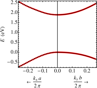
Ab-initio calculation and tight binding fit for GeS - Due to the lack of tight binding models for monochalcogenide materials Singh and Hennig (2014); Gomes and Carvalho (2015), we have derived the tight binding parameters by fitting the electronic structure of GeS ab-initio. We used the PBE Perdew et al. (1996) approximation to the exchange correlation functional, ultrasoft pseudopotentials, Garrity et al. (2014) Quantum-ESPRESSO Giannozzi et al. (2009) and Wannier90 Mostofi et al. (2008) computer packages. The cutoff for electron wavefunction is set to 40 Ry and cutoff for electron density to 200 Ry. Internal coordinates and in-plane lattice constants were fully relaxed. Vacuum region between repeating images of GeS monolayers is 17 . Wannier functions were constructed from a 12x12 regular k-mesh grid. The maximally localized Wannier functions were constructed in a standard way by projecting into hydrogenic s-like and p-like orbitals on both Ge and S atoms along with two s-like orbitals in the vacuum region that are needed to represent the vacuum states. The frozen window for the disentanglement procedure spans up to 6.2 eV above the Fermi level. The crystal structure of GeS is orthorombic with space group Pnma (No. 62) and lattice vectors and , with and and contains two Ge and two S atoms. The structure can be seen as two GeS zigzag chains separated by a height of . The ab-initio results for the conduction and valence bands near the point are shown in Fig. 4 and have mostly character.
This system can be effectively described with a two site tight binding model. This can be done because the lattice structure has glide symmetries with mirror reflection and translations and , with and . When the out of plane positions of the atoms are not relevant for the problem of interest, one can define a smaller two site unit cell where the glides play the role of lattice vectors (as it is done in black phosphorus Ezawa (2014)). The Ge and S sites in this effective tight binding model are located at and , with .This is the tight binding model employed in the main text. The parameters of this model are obtained from the ab-initio calculation as follows.
Since our aim is to model faithfully only the low energy bands around the Gamma point, it will suffice to consider a single orbital per site in the tight binding model. The minimal model parameters are the on-site potential difference between Ge and S orbitals and the three nearest neighbors hoppings , with , which are all between Ge and S atoms. In addition, to reproduce the small particle-hole asymmetry of the gap, we also consider two further neighbor hoppings and which connect Ge-Ge or S-S pairs (we assume the same values for both species to simplify).
The tight binding Hamiltonian takes the form with coefficients
| (28) | ||||
| (29) | ||||
| (30) |
where, as defined in the text, . Our tight binding fit is intended to reproduce faithfully the bands and wavefunctions close to the band edge, where the effective low energy model applies. This model is given by
| (31) |
where a constant term is omitted as it can be absorbed in the chemical potential. The effective model parameters are related to the tight binding parameters as
| (32) | ||||
| (33) | ||||
| (34) | ||||
| (35) | ||||
| (36) | ||||
| (37) |
The key to obtain a reliable tight binding parametrization is that, since the shift current depends sensitively on the actual wavefunctions, the tight binding model should be fitted to wavefunction dependent quantities in addition to the band energies. The simplest gauge invariant quantity that depends on wavefunction phases is the bracket of two covariant derivatives
| (38) |
with , with the Berry connection. The real and imaginary parts of this tensor are known as the Berry curvature and the quantum metric. A fit that reproduces this tensor correctly in addition to band energies ensures that the wavefunction structure around the point is correctly accounted for, so that any other gauge invariant quantity computed in the effective model should be the same as that computed ab-initio.
| Ab-initio input parameters | ||||||
|---|---|---|---|---|---|---|
| 1.89 eV | -0.064 | 0.079 | -0.340 | 0.171 | 3.565 | 2.529 |
| Tight binding parameters | ||||||
| 0.41 eV | -2.33 eV | 0.61 eV | 0.13 eV | 0.07 eV | -0.09 eV | 0.52 |
The Berry curvature is defined as
| (39) |
The Berry curvature around for the tight binding model is given by
| (40) |
Since vanishes at the origin, we take as one extra input for the fit. The quantum metric is defined as
| (41) |
The only non-vanishing component of the quantum metric at is given by
| (42) |
so we take as another extra input for the fit.
In summary, we take as ab-initio input parameters the gap, the four effective masses, and the lowest order Berry curvature and quantum metric, and . The difference in effective masses for electron and hole bands, accounted for the term , can be fitted independently with the hoppings and . Since has no impact in the shift current response, the hoppings and are not considered in the main text. The rest of the input is fitted with , and , the on-site potential and , and the results of the fit are shown in Table 1. While is in fact known from the lattice structure of GeS to be , obtaining it independently from the tight binding fit, which gives a close value of provides an additional check of the validity of the model.
Acknowledgments - We acknowledge useful discussions with J. Sipe, E. J. Mele, M. Bernardi, P. Král, S. Barraza-Lopez and F. Duque-Gomez and especially with Y. Xu. We also thank R. Ilan and A.G. Grushin for a careful reading of the manuscript. BMF was supported by Conacyt, NSF DMR-12065135 and NERSC Contract No. DE-AC02-05CH11231, AMC was supported by the NSERC CGS-MSFSS and the NSERC CGS-D3, F. de Juan was supported by the U.S. Department of Energy, Office of Science, Basic Energy Sciences, Materials Sciences and Engineering Division, grant DE-AC02-05CH11231, and J.E.M. was supported by AFOSR MURI.
Author contributions - AMC and BMF contributed equally to the work. AMC, BMF, FJ and JEM carried out the analytical and numerical analysis. SC carried out all ab-initio computations. All authors contributed to the results and the writing of the manuscript.
Data availability - The data that support the findings of this study are available from the corresponding author upon request.
Competing financial interests - The authors declare no competing financial interests.
Correspondence - Correspondence and requests for materials should be addressed to J.E.M. (email: jemoore@berkeley.edu)
References
- Shockley and Queisser (1961) William Shockley and Hans J. Queisser, “Detailed balance limit of efficiency of pn junction solar cells,” J. Appl. Phys. 32, 510 (1961).
- Kraut and von Baltz (1979) Wolfgang Kraut and Ralph von Baltz, “Anomalous bulk photovoltaic effect in ferroelectrics: A quadratic response theory,” Phys. Rev. B 19, 1548–1554 (1979).
- Belinicher and Sturman (1980) V I Belinicher and B I Sturman, “The photogalvanic effect in media lacking a center of symmetry,” Sov. Phys. Usp. 23, 199 (1980).
- von Baltz and Kraut (1981) Ralph von Baltz and Wolfgang Kraut, “Theory of the bulk photovoltaic effect in pure crystals,” Phys. Rev. B 23, 5590 (1981).
- Presting and Von Baltz (1982) H. Presting and R. Von Baltz, “Bulk photovoltaic effect in a ferroelectric crystal a model calculation,” Phys. Status Solidi (b) 112, 559–564 (1982).
- Sturman and Sturman (1992) Boris I. Sturman and Paul J. Sturman, Photovoltaic and Photo-refractive Effects in Noncentrosymmetric Materials (CRC Press, 1992).
- Aversa and Sipe (1995) Claudio Aversa and J. E. Sipe, “Nonlinear optical susceptibilities of semiconductors: Results with a length-gauge analysis,” Phys. Rev. B 52, 14636–14645 (1995).
- Kristoffel et al. (1982) N. Kristoffel, R. von Baltz, and D. Hornung, “On the intrinsic bulk photovoltaic effect: Performing the sum over intermediate states,” Z. Physik 47, 293–296 (1982).
- Sipe and Shkrebtii (2000) J. E. Sipe and A. I. Shkrebtii, “Second-order optical response in semiconductors,” Phys. Rev. B 61, 5337 (2000).
- Král et al. (2000) Petr Král, E. J. Mele, and David Tománek, “Photogalvanic effects in heteropolar nanotubes,” Phys. Rev. Lett. 85, 1512 (2000).
- Ji et al. (2010) Wei Ji, Kui Yao, and Yung C. Liang, “Bulk photovoltaic effect at visible wavelength in epitaxial ferroelectric bifeo3 thin films,” Adv. Mater. 22, 1763–1766 (2010).
- Zheng et al. (2015) Fan Zheng, Hiroyuki Takenaka, Fenggong Wang, Nathan Z. Koocher, and Andrew M. Rappe, “First-principles calculation of the bulk photovoltaic effect in ch3nh3pbi3 and ch3nh3pbi3–xclx,” J. Phys. Chem. Lett. 6, 31–37 (2015).
- Young and Rappe (2012) Steve M. Young and Andrew M. Rappe, “First principles calculation of the shift current photovoltaic effect in ferroelectrics,” Phys. Rev. Lett. 109, 116601 (2012).
- Brehm et al. (2014) John A Brehm, Steve M Young, Fan Zheng, and Andrew M Rappe, “First-principles calculation of the bulk photovoltaic effect in the polar compounds liass2, liasse2, and naasse2,” J. Chem. Phys. 141, 204704 (2014).
- Hodes (2013) Gary Hodes, “Perovskite-based solar cells,” Science 342, 317 (2013).
- Egger et al. (2015) David A. Egger, Eran Edri, David Cahen, and Gary Hodes, “Perovskite solar cells: Do we know what we do not know?” J. Phys. Chem. Lett. 6, 279–282 (2015).
- McGehee (2014) Michael D. McGehee, “Perovskite solar cells: Continuing to soar,” Nat. Mater. 13, 845–846 (2014).
- Antonietta Loi and Hummelen (2013) Maria Antonietta Loi and Jan C. Hummelen, “Hybrid solar cells: Perovskites under the sun,” Nat. Mater. 12, 1087–1089 (2013).
- Even et al. (2013) Jacky Even, Laurent Pedesseau, Jean-Marc Jancu, and Claudine Katan, “Importance of spin–orbit coupling in hybrid organic/inorganic perovskites for photovoltaic applications,” J. Phys. Chem. Lett. 4, 2999–3005 (2013).
- Stroppa et al. (2014) Alessandro Stroppa, Domenico Di Sante, Paolo Barone, Menno Bokdam, Georg Kresse, Cesare Franchini, Myung-Hwan Whangbo, and Silvia Picozzi, “Tunable ferroelectric polarization and its interplay with spin–orbit coupling in tin iodide perovskites,” Nat. Commun. 5, 5900 (2014).
- Zhang et al. (2015a) C. Zhang, D. Sun, C-X. Sheng, Y. X. Zhai, K. Mielczarek, A. Zakhidov, and Z. V. Vardeny, “Magnetic field effects in hybrid perovskite devices,” Nat. Phys. 11, 427–434 (2015a).
- Saba et al. (2014) Michele Saba, Michele Cadelano, Daniela Marongiu, Feipeng Chen, Valerio Sarritzu, Nicola Sestu, Cristiana Figus, Mauro Aresti, Roberto Piras, Alessandra Geddo Lehmann, Carla Cannas, Anna Musinu, Francesco Quochi, Andrea Mura, and Giovanni Bongiovanni, “Correlated electron–hole plasma in organometal perovskites,” Nat. Commun. 5, 5049 (2014).
- Leguy et al. (2015) Aurelien M. A. Leguy, Jarvist Moore Frost, Andrew P. McMahon, Victoria Garcia Sakai, W. Kockelmann, ChunHung Law, Xiaoe Li, Fabrizia Foglia, Aron Walsh, Brian C. O’Regan, Jenny Nelson, Joao T. Cabral, and Piers R. F. Barnes, “The dynamics of methylammonium ions in hybrid organic-inorganic perovskite solar cells,” Nat. Commun. 6, 7124 (2015).
- Motta et al. (2015) Carlo Motta, Fedwa El-Mellouhi, Sabre Kais, Nouar Tabet, Fahhad Alharbi, and Stefano Sanvito, “Revealing the role of organic cations in hybrid halide perovskite ch3nh3pbi3,” Nat. Commun. 6, 7026 (2015).
- Filip et al. (2014) Marina R. Filip, Giles E. Eperon, Henry J. Snaith, and Feliciano Giustino, “Steric engineering of metal-halide perovskites with tunable optical band gaps,” Nat. Commun. 5, 5757 (2014).
- Saidaminov et al. (2015) Makhsud I. Saidaminov, Ahmed L. Abdelhady, Banavoth Murali, Erkki Alarousu, Victor M. Burlakov, Wei Peng, Ibrahim Dursun, Lingfei Wang, Yao He, Giacomo Maculan, Alain Goriely, Tom Wu, Omar F. Mohammed, and Osman M. Bakr, “High-quality bulk hybrid perovskite single crystals within minutes by inverse temperature crystallization,” Nat. Commun. 6, 7586 (2015).
- Eames et al. (2015) Christopher Eames, Jarvist M. Frost, Piers R. F. Barnes, Brian C. O/’Regan, Aron Walsh, and M. Saiful Islam, “Ionic transport in hybrid lead iodide perovskite solar cells,” Nat. Commun. 6, 7497 (2015).
- Heo et al. (2013) Jin Hyuck Heo, Sang Hyuk Im, Jun Hong Noh, Tarak N. Mandal, Choong-Sun Lim, Jeong Ah Chang, Yong Hui Lee, Hi-jung Kim, Arpita Sarkar, NazeeruddinMd. K., Michael Gratzel, and Sang Il Seok, “Efficient inorganic-organic hybrid heterojunction solar cells containing perovskite compound and polymeric hole conductors,” Nat. Photon. 7, 486–491 (2013).
- Young et al. (2012) Steve M. Young, Fan Zheng, and Andrew M. Rappe, “First-principles calculation of the bulk photovoltaic effect in bismuth ferrite,” Phys. Rev. Lett. 109, 236601 (2012).
- Wang et al. (2015) F. Wang, S. M. Young, F. Zheng, I. Grinberg, and A. M. Rappe, “Bulk photovoltaic effect enhancement via electrostatic control in layered ferroelectrics,” (2015), arXiv:1503.00679 .
- Wang and Rappe (2015) Fenggong Wang and Andrew M. Rappe, “First-principles calculation of the bulk photovoltaic effect in and (k,ba)(ni,nb),” Phys. Rev. B 91, 165124 (2015).
- Mahan and Sofo (1996) G.D. Mahan and J.O. Sofo, “The best thermoelectric,” Proc. Natl. Acad. Sci. USA 93, 7436 (1996).
- DiSalvo (1999) F. J. DiSalvo, “Thermoelectric cooling and power generation,” Science 285, 703–706 (1999).
- Murphy et al. (2008) Padraig Murphy, Subroto Mukerjee, and Joel Moore, “Optimal thermoelectric figure of merit of a molecular junction,” Phys. Rev. B 78, 161406 (2008).
- Van Hove (1953) Léon Van Hove, “The occurrence of singularities in the elastic frequency distribution of a crystal,” Phys. Rev. 89, 1189–1193 (1953).
- Nalwa (1995) Hari Singh Nalwa, ed., Ferroelectric Polymers: Chemistry: Physics, and Applications (CRC Press, 1995).
- Lovinger (1983) Andrew J Lovinger, “Ferroelectric polymers,” Science 220, 1115–1121 (1983).
- Gontia et al. (1999) I. Gontia, S. V. Frolov, M. Liess, E. Ehrenfreund, Z. V. Vardeny, K. Tada, H. Kajii, R. Hidayat, A. Fujii, K. Yoshino, M. Teraguchi, and T. Masuda, “Excitation dynamics in disubstituted polyacetylene,” Phys. Rev. Lett. 82, 4058–4061 (1999).
- Rice and Mele (1982) M. J. Rice and E. J. Mele, “Elementary excitations of a linearly conjugated diatomic polymer,” Phys. Rev. Lett. 49, 1455–1459 (1982).
- Geim and Grigorieva (2013) AK Geim and IV Grigorieva, “Van der waals heterostructures,” Nature 499, 419–425 (2013).
- Britnell et al. (2013) L. Britnell, R. M. Ribeiro, A. Eckmann, R. Jalil, B. D. Belle, A. Mishchenko, Y.-J. Kim, R. V. Gorbachev, T. Georgiou, S. V. Morozov, A. N. Grigorenko, A. K. Geim, C. Casiraghi, A. H. Castro Neto, and K. S. Novoselov, “Strong light-matter interactions in heterostructures of atomically thin films,” Science 340, 1311–1314 (2013).
- Yu et al. (2013) Woo Jong Yu, Yuan Liu, Hailong Zhou, Anxiang Yin, Zheng Li, Yu Huang, and Xiangfeng Duan, “Highly efficient gate-tunable photocurrent generation in vertical heterostructures of layered materials,” Nature Nanotech. 8, 952–958 (2013).
- Bernardi et al. (2013) Marco Bernardi, Maurizia Palummo, and Jeffrey C Grossman, “Extraordinary sunlight absorption and one nanometer thick photovoltaics using two-dimensional monolayer materials,” Nano lett. 13, 3664–3670 (2013).
- Buscema et al. (2014) Michele Buscema, Dirk J Groenendijk, Gary A Steele, Herre SJ van der Zant, and Andres Castellanos-Gomez, “Photovoltaic effect in few-layer black phosphorus pn junctions defined by local electrostatic gating,” Nature Commun. 5 (2014).
- Singh and Hennig (2014) Arunima K Singh and Richard G Hennig, “Computational prediction of two-dimensional group-iv mono-chalcogenides,” Appl. Phys. Lett. 105, 042103 (2014).
- Gomes and Carvalho (2015) Lidia C Gomes and A Carvalho, “Phosphorene analogues: isoelectronic two-dimensional group-iv monochalcogenides with orthorhombic structure,” arXiv:1504.05627 (2015).
- Antunez et al. (2011) Priscilla D Antunez, Jannise J Buckley, and Richard L Brutchey, “Tin and germanium monochalcogenide iv–vi semiconductor nanocrystals for use in solar cells,” Nanoscale 3, 2399–2411 (2011).
- Li et al. (2016) Feng Li, Xiuhong Liu, Yu Wang, and Yafei Li, “Germanium monosulfide monolayer: a novel two-dimensional semiconductor with a high carrier mobility,” J. Mater. Chem. C 4, 2155–2159 (2016).
- Rodin et al. (2016) A. S. Rodin, Lidia C. Gomes, A. Carvalho, and A. H. Castro Neto, “Valley physics in tin (ii) sulfide,” Phys. Rev. B 93, 045431 (2016).
- Li et al. (2012) Chun Li, Liang Huang, Gayatri Pongur Snigdha, Yifei Yu, and Linyou Cao, “Role of boundary layer diffusion in vapor deposition growth of chalcogenide nanosheets: The case of ges,” ACS Nano 6, 8868–8877 (2012).
- Ulaganathan et al. (2016) Rajesh Kumar Ulaganathan, Yi-Ying Lu, Chia-Jung Kuo, Srinivasa Reddy Tamalampudi, Raman Sankar, Karunakara Moorthy Boopathi, Ankur Anand, Kanchan Yadav, Roshan Jesus Mathew, Chia-Rung Liu, et al., “High photosensitivity and broad spectral response of multi-layered germanium sulfide transistors,” Nanoscale 8, 2284–2292 (2016).
- Vaughn II et al. (2010) Dimitri D Vaughn II, Romesh J Patel, Michael A Hickner, and Raymond E Schaak, “Single-crystal colloidal nanosheets of ges and gese,” J. Amer. Chem. Soc. 132, 15170–15172 (2010).
- Ramasamy et al. (2016) Parthiban Ramasamy, Dohyun Kwak, Da-Hye Lim, Hyun-Soo Ra, and Jong-Soo Lee, “Solution synthesis of ges and gese nanosheets for high-sensitivity photodetectors,” J. Mater. Chem. C 4, 479–485 (2016).
- Brent et al. (2015) Jack R Brent, David J Lewis, Tommy Lorenz, Edward A Lewis, Nicky Savjani, Sarah J Haigh, Gotthard Seifert, Brian Derby, and Paul O’Brien, “Tin (ii) sulfide (sns) nanosheets by liquid-phase exfoliation of herzenbergite: Iv–vi main group two-dimensional atomic crystals,” J. Amer. Chem. Soc. 137, 12689–12696 (2015).
- Xia et al. (2016) Jing Xia, Xuan-Ze Li, Xing Huang, Nannan Mao, Dan-Dan Zhu, Lei Wang, Hua Xu, and Xiang-Min Meng, “Physical vapor deposition synthesis of two-dimensional orthorhombic sns flakes with strong angle/temperature-dependent raman responses,” Nanoscale 8, 2063–2070 (2016).
- Li et al. (2013) Lun Li, Zhong Chen, Ying Hu, Xuewen Wang, Ting Zhang, Wei Chen, and Qiangbin Wang, “Single-layer single-crystalline snse nanosheets,” J. Am. Chem. Soc. 135, 1213–1216 (2013).
- Zhang et al. (2015b) Jian Zhang, Hongyang Zhu, Xiaoxin Wu, Hang Cui, Dongmei Li, Junru Jiang, Chunxiao Gao, Qiushi Wang, and Qiliang Cui, “Plasma-assisted synthesis and pressure-induced structural transition of single-crystalline snse nanosheets,” Nanoscale 7, 10807–10816 (2015b).
- Zhao et al. (2015) Shuli Zhao, Huan Wang, Yu Zhou, Lei Liao, Ying Jiang, Xiao Yang, Guanchu Chen, Min Lin, Yong Wang, Hailin Peng, et al., “Controlled synthesis of single-crystal snse nanoplates,” Nano Research 8, 288–295 (2015).
- Bena and Montambaux (2009) Cristina Bena and Gilles Montambaux, “Remarks on the tight-binding model of graphene,” New J. Phys. 11, 095003 (2009).
- Dobardić et al. (2015) E Dobardić, M Dimitrijević, and MV Milovanović, “Generalized bloch theorem and topological characterization,” Phys. Rev. B 91, 125424 (2015).
- Fruchart et al. (2014) Michel Fruchart, David Carpentier, and Krzysztof Gawedzki, “Parallel transport and band theory in crystals,” Europhys. Lett. 106, 60002 (2014).
- Banerjee et al. (2009) S Banerjee, RRP Singh, V Pardo, and WE Pickett, “Tight-binding modeling and low-energy behavior of the semi-dirac point,” Phys. Rev. Lett. 103, 016402 (2009).
- Su et al. (1979) W. P. Su, J. R. Schrieffer, and A. J. Heeger, “Solitons in polyacetylene,” Phys. Rev. Lett. 42, 1698–1701 (1979).
- Xia et al. (2014) Fengnian Xia, Han Wang, and Yichen Jia, “Rediscovering black phosphorus as an anisotropic layered material for optoelectronics and electronics,” Nature Commun. 5 (2014).
- Liu et al. (2015) Erfu Liu, Yajun Fu, Yaojia Wang, Yanqing Feng, Huimei Liu, Xiangang Wan, Wei Zhou, Baigeng Wang, Lubin Shao, Ching-Hwa Ho, et al., “Integrated digital inverters based on two-dimensional anisotropic res2 field-effect transistors,” Nature Commun. 6 (2015).
- Rudenko and Katsnelson (2014) A. N. Rudenko and M. I. Katsnelson, “Quasiparticle band structure and tight-binding model for single- and bilayer black phosphorus,” Phys. Rev. B 89, 201408 (2014).
- Rudenko et al. (2015) AN Rudenko, Shengjun Yuan, and MI Katsnelson, “Toward a realistic description of multilayer black phosphorus: from approximation to large-scale tight-binding simulations,” arXiv:1506.01954 (2015).
- Ezawa (2014) Motohiko Ezawa, “Topological origin of quasi-flat edge band in phosphorene,” New J. Phys. 16, 115004 (2014).
- Montambaux et al. (2009) G. Montambaux, F. Piéchon, J.-N. Fuchs, and M. O. Goerbig, “Merging of dirac points in a two-dimensional crystal,” Phys. Rev. B 80, 153412 (2009).
- Pagliaro et al. (2008) Mario Pagliaro, Giovanni Palmisano, and Rosaria Ciriminna, Flexible solar cells (Wiley, 2008).
- Perdew et al. (1996) John P. Perdew, Kieron Burke, and Matthias Ernzerhof, “Generalized gradient approximation made simple,” Phys. Rev. Lett. 77, 3865–3868 (1996).
- Garrity et al. (2014) Kevin F. Garrity, Joseph W. Bennett, Karin M. Rabe, and David Vanderbilt, “Pseudopotentials for high-throughput {DFT} calculations,” Comput. Mater. Sci. 81, 446 – 452 (2014).
- Giannozzi et al. (2009) Paolo Giannozzi et al., “Quantum espresso: a modular and open-source software project for quantum simulations of materials,” J. Phys.:Condens. Matter 21, 395502 (2009).
- Mostofi et al. (2008) Arash A. Mostofi, Jonathan R. Yates, Young-Su Lee, Ivo Souza, David Vanderbilt, and Nicola Marzari, “wannier90: A tool for obtaining maximally-localised wannier functions,” Comput. Phys. Commun. 178, 685 – 699 (2008).