A physics based model of gate tunable metal-graphene contact resistance benchmarked against experimental data
Abstract
The metal-graphene contact resistance is a technological bottleneck for the realization of viable graphene based electronics. We report a useful model to find the gate tunable components of this resistance determined by the sequential tunneling of carriers between the 3D-metal and 2D-graphene underneath followed by Klein tunneling to the graphene in the channel. This model quantifies the intrinsic factors that control that resistance, including the effect of unintended chemical doping. Our results agree with experimental results for several metals.
Keywords: Graphene; Metal-Graphene junction; Contact resistance; Contact resistivity; Graphene field-effect-transistor.
1 Introduction
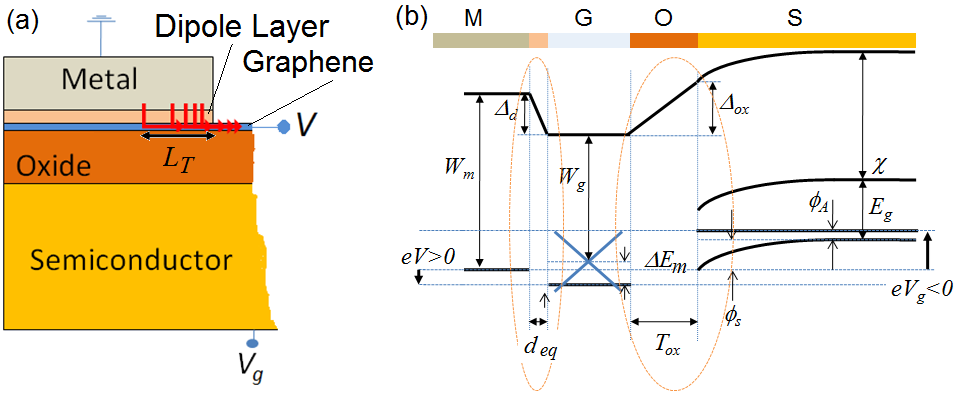
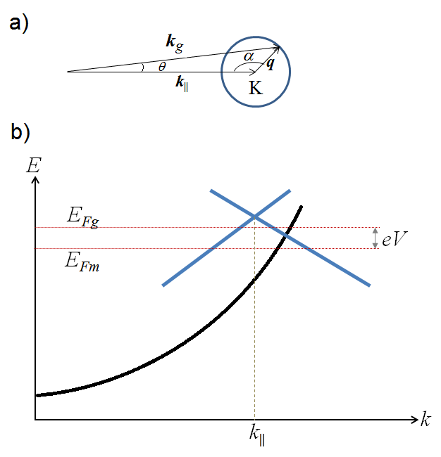
While graphene has emerged as a promising material for future electronic devices thanks to its unique electronic properties, the metal-graphene contact resistance () remains a limiting factor for graphene-based electronic devices 1. In particular, for high frequency electronics it is an issue very much influencing figures of merit like the maximum frequency of oscillation, the cutoff frequency, or the intrinsic gain 2. Therefore it is neccesary to understand the intrinsic and extrinsic factors determining , which displays a strong variation depending on the metal contact and fabrication procedure details3, 4, 5. To gain understanding of these factors so that a better control of the contact’s technology is feasible, a comprehensive physics based model of is an absolute requirement. One relevant model was already proposed by Xia et al.6 to describe the transport in metal-graphene junctions as two sequential tunneling process from the metal to graphene over an effective transfer length (), followed by injection to the graphene channel (see Fig. 1a). However, there is an important ingredient determining namely, the transmission from a 3D system (metal) to a 2D system (graphene), that has so far not been taken into account properly there in a physics basis. Evidence of the current crowding effect over has been reported by Sundaram et al. using photocurrent spectroscopy 7.
In order to improve the current understanding, we have considered the issue of the carriers transmission between materials of different dimensionality. Specifically, we have developed a physics-based model where the first process is responsible for the resistance between the metal and the graphene underneath () and the second process includes the resistance due to a potential step across the junction formed between the graphene under the metal and the graphene channel (). The total contact resistance is then the series combination of both contributions, , accounting for any current crowding effect near the contact edge. The calculation of and are based on the Bardeen Transfer Hamiltonian (BTH) method 8, 9 and the Landauer approach 10, respectively. The BTH method allows us to get information about the matrix elements for the transition between 3D-metal and 2D-graphene states and combined with Fermi’s golden rule, yields a compact expression for the specific contact resistivity . On the other hand, the Landauer approach allows to get the conductance of carriers across the potential step between the graphene under the metal and the graphene in the channel, where the angular dependence transmission of Dirac fermions and the effective length of the potential have been taken into account. To model we have considered it as a building block of a FET device, so its value will strongly depend on the applied gate voltage.
2 Methods
2.1 Electrostatics
In this paper we start with the graphene electrostatics. We considered a three terminal graphene FET (GFET) device controlled by a global back-gate voltage as sketched in Fig. 1a, although it could be easily adapted to a device with both top- and back-gates as we will show later on. We split the electrostatic problem by considering two 1D heterostructures, namely, the Metal/Graphene/Oxide/Semiconductor (MGOS) and Graphene/Oxide/Semiconductor (GOS) heterostructures in the contact and channel regions, respectively. In Fig. 1b the corresponding band diagram of the MGOS heterostructure has been shown. In each of these regions we model the gate voltage dependence of the graphene Fermi level relative to its Dirac energy, namely and for the graphene under the metal and graphene in the channel, respectively. The energy potential loops at the encircled interfaces in Fig. 1b together with the Gauss’s law are considered, resulting in Eqs. 1a-c. Because of the charge transfer between the metal and graphene, a dipole layer of size inside the equilibrium separation distance is set up11. Also a difference between the metal and the graphene Fermi level in the contact region, supplied by the drain terminal, has been assumed. The work-functions of the metal and graphene are and , respectively.
| (1a) | |||
| (1b) | |||
| (1c) | |||
In Eq. 1a, the term is the potential drop in the dipole layer which can be expressed as , where corresponds to the charge transfer and to chemical potential interaction describing the short range interaction from the overlap of the metal and graphene wavefunctions 11, 12. In Eq. 1b, the back-gate voltage is referred to the source metal electrode potential, is the semiconductor work-function and is the semiconductor surface potential. In Eq. 1c, describes the charge per unit area induced in the surface metal, is the net charge sheet density within the graphene layer 13 plus the charge density due to possible chemical doping14 () and describes the charge per unit area induced in the semiconductor. Here, and describe the capacitive coupling to the metal and back gate, respectively. The value of can differ from the equilibrium distance (nm) due to the spatial extension of the carbon and metal orbitals. The value of strongly depends on the separation distance and it becomes negligible for nm 11. Combining Eqs. 1 and assuming that saturates at strong inversion and acummulation, we get a simple quadratic equation for :
| (2) |
where , with cm/s) the Fermi velocity, and
| (3) |
represents the Dirac gate voltage required to achieve and defines the back-gate voltage value for which and the resistance become maximum, as we will see later.
Because the dipole layer has been modeled as an insulator, the channel region electrostatics under the influence of both top- and back-gates can be described in a similar way as presented in Eqs. 1, so the Fermi level shift in the channel () can be obtained from:
| (4) |
with
| (5) |
In the last equations, and are the back (top)- capacitance and gate voltage, respectively. The new Dirac voltage must be understood as the back-gate voltage needed to achieve at a fixed top-gate voltage . When there is only a back-gate, like in our experimental devices, we can get for the GOS structure simply setting .
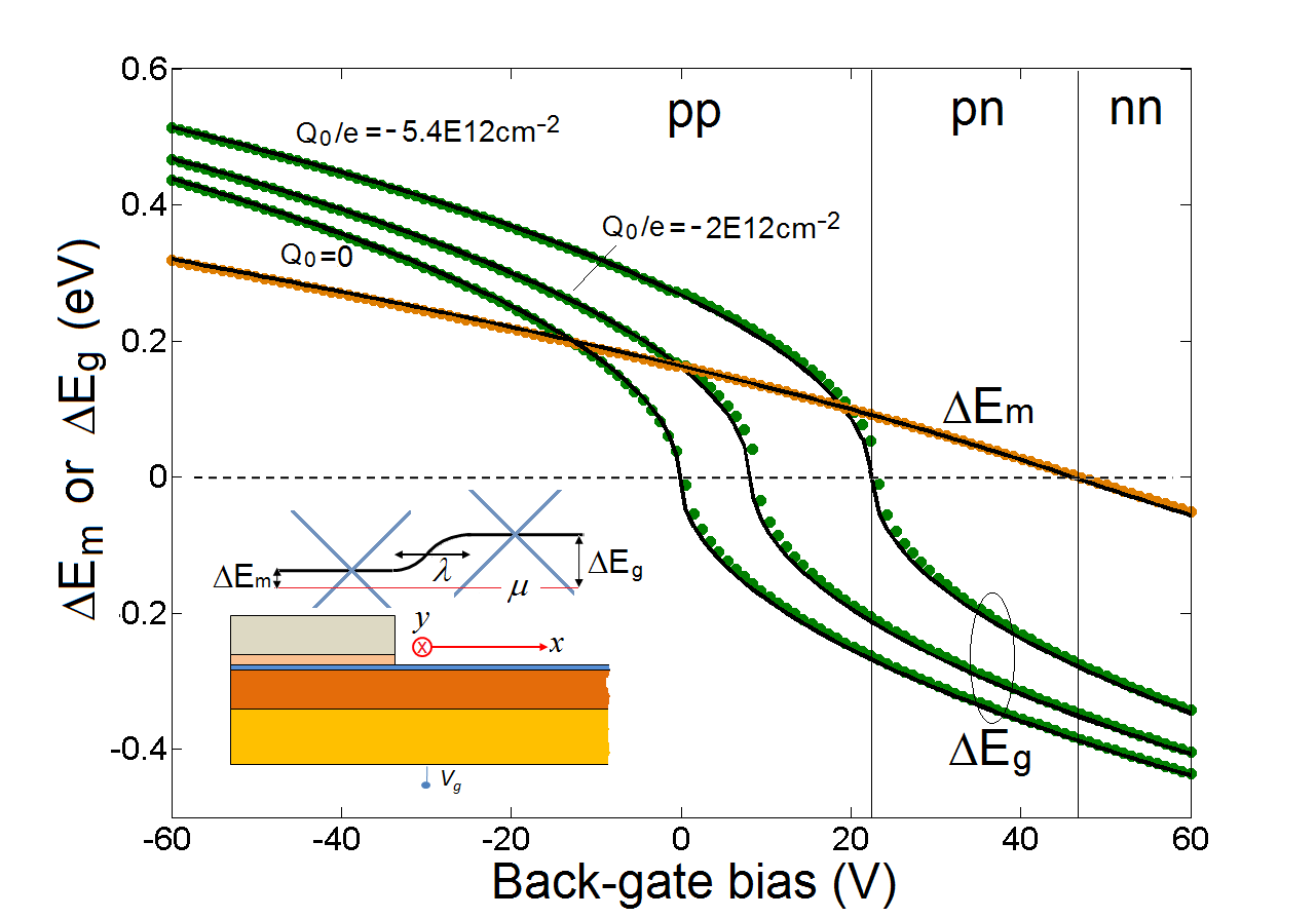
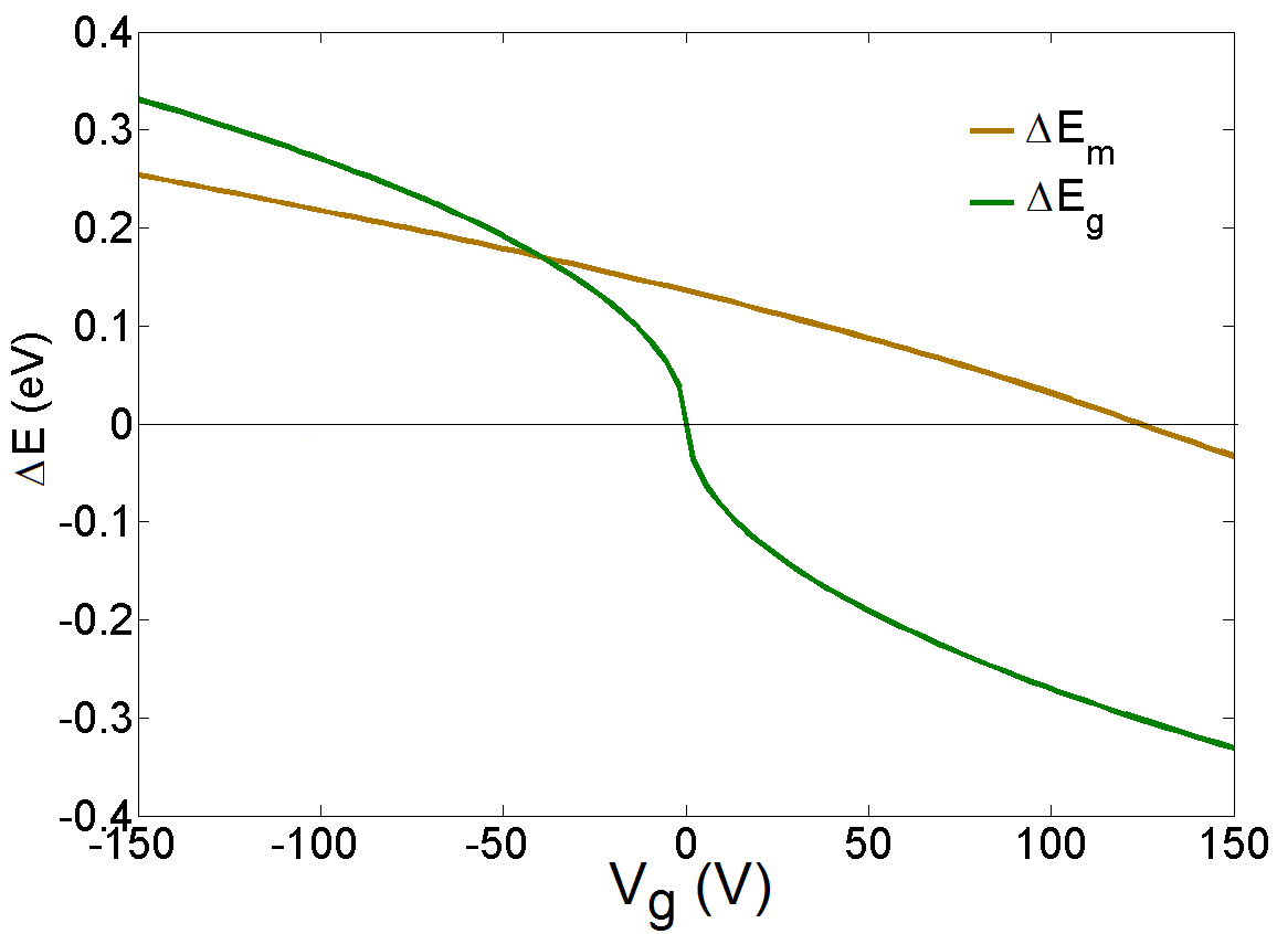
With the electrostatic model given by the above equations, the key quantities and could be determined, which in turn are needed to calculate the contact resistance. Fig. 2 shows both and at equilibrium as a function of the back-gate bias using Palladium (Pd) as metal electrode and SiO2 as oxide with thickness nm. This can be done either by solving Eqs. 1 or the simplified Eq. 2, with a very little difference between them. Different kinds of junctions may build-up depending on the back-gate bias, namely pp-type, pn-type, and nn-type. Here, we have assumed that is only affecting the graphene channel, and not the graphene underneath the metal. The impact of in determining the crossing of with zero, can be seen in the figure. To capture the transition between the pp-type and pn-type junction, which was observed at V6, the parameter was set to cm-2. Next transistion produced between the pn-type and nn-type junction was captured by our model at V, in accordance with the experiment of Xia et al. The electrical parameters that we have assumed for all the simulations presented in this work are shown in Table I. Because of charge transfer between the graphene underneath the metal and the graphene in the channel, a potential step of effective length arises at the contact edge. An sketch of that potential step is illustrated in Fig. 2. Once we get the electrostatic model, we are now ready to discuss how to model the contact resistance.
2.2 Resistance and resistivity
The procedure to model is based on the Transmission Line Method 15, 16, 17, which in turn requires determination of , namely:
| (6) |
where represents the specific contact resistivity, (250 in this work) is the graphene sheet resistance under the metal, is the characteristic length over which current injection occurs between the metal and the graphene layer (transfer length), and is the length (width) of the contact. Here, is calculated by means of the BTH method, which allows us to split the metal-graphene system into separate metal and graphene subsystems with known Hamiltonians. In the framework of the BTH method, the probability of elastic tunneling is calculated using Fermi’s golden rule. This gives a quantitative estimate of the coupling between the metal and graphene states, so it is possible to get an analytical formula with key parameters for as a function of . In the Supplementary data we show how to calculate from the tunneling current density using the BTH approach. The resulting compact analytical expression for as a function of under the metal at , for a given temperature can be written as:
| (7) |
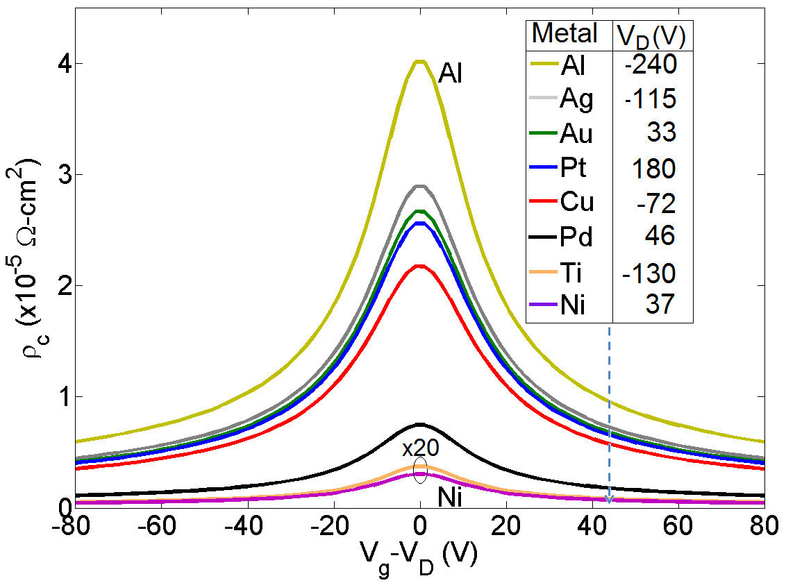
where , with and the effective electron mass in the metal and dipole layer, respectively. The factor is the electron decay constant in the dipole layer and has the form 13, where has been taken as the barrier height and is the parallel momentum at the K or K′ points (i.e., ). For a typical metal the work-function is eV so nm-1. As a consequence eV and eV. From Eq. 7 we can infer that the maximum value of depends exponentially on the equilibrium separation distance and that the maximum resistivity is located at (). Fig. 3 shows at K as a function of the back-gate bias overdrive () considering different metals. After sorting the metals by their peak contact resistivity, it appears that is the main factor controlling it, being the Ni contact the best option, followed by Ti. Here we have assumed SiO2 as the insulator with nm and equal effective masses for every metal. According to Table I, the Ni-graphene (Al-graphene) contact has the smallest (largest) equilibrium distance of the metals here represented, giving rise to the smallest (largest) value of at . The values of predicted from Eq. 7 are consistent with experimental results reported by Nagashio and Berdebes 18, 19 for Ni, Ti and Pd. Although the Ni happens to be the best option to get the lowest , other effects that contribute to the lateral resistance must be considered. As a matter of fact, for Ni can become comparable to that of Pd, as we will show later. Our model predicts how depends on factors like the workfunction difference, the equilbrium distance, the chemical interaction potential, the gate capacitance and the temperature.
| Metal | |||
|---|---|---|---|
| Ni | 5.47 | 2.05 | 0.8∗ |
| Ti | 4.65 | 2.10 | 0.9∗ |
| Pd | 5.67 | 3.00 | 0.90 |
| Cu | 5.22 | 3.26 | 0.99 |
| Pt | 6.13 | 3.30 | 0.93 |
| Au | 5.54 | 3.31 | 0.91 |
| Ag | 4.92 | 3.33 | 0.88 |
| Al | 4.22 | 3.41 | 0.77 |
2.3 Resistance
Next, we model the lateral contact resistance across a potential step with effective length (see inset of Fig. 2) relying on the Landauer approach. The potential along the transport direction can be described by a simple space-dependent Fermi level shift10:
| (8) |
where we have considered that the metal electrode cover the left half-plane (). The type ( or ) and density of carriers in both left and right half-planes are tuned by the back-gate. The important quantity to be determined is the reflection probability of Dirac fermions across the potential step, which has been derived by Cayssol et al.10, namely:
| (9) |
where the momenta with The longitudinal momentum is related to the transversal momentum by the phytagorean relationship
| (10) |
where the positive (negative) sign indicates that the doping is type.
By means of the Landauer formula the conductance can be obtained from:
| (11) |
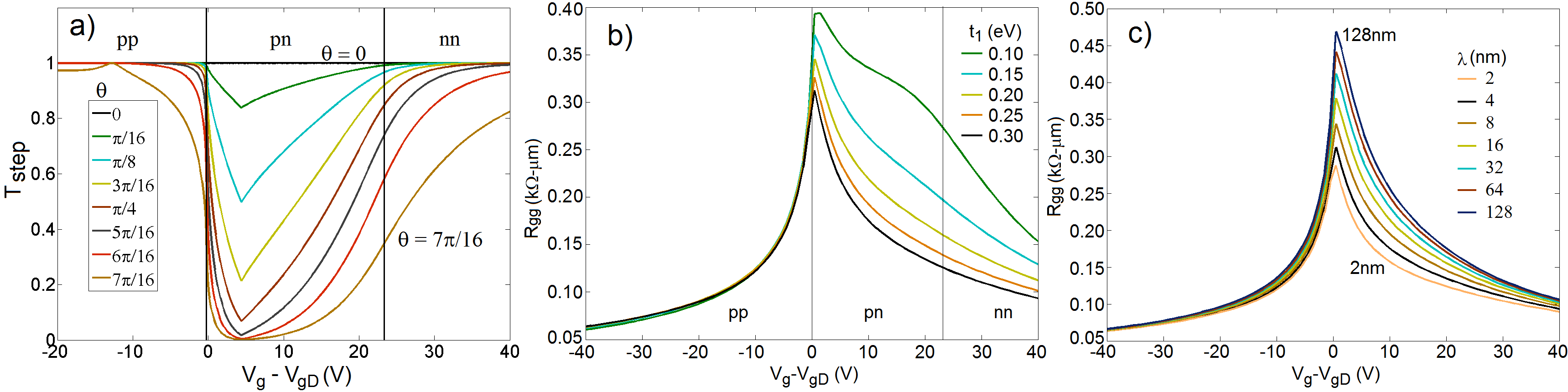
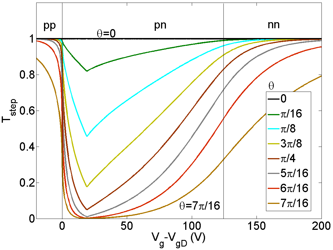
where is the transmission probability and . Fig. 4a shows the transmission probability of the Dirac fermions across the potential step as a function of for different incidence angles assuming Pd as the metal. In particular, it indicates the absence of backscattering at normal incidence ( or ), because of the orthogonality of incoming and reflected spinor states. In contrast, the transmission of the bipolar contacts (case ) tends toward zero for incident carriers when .
So far we have not considered the effect of the drain bias () in defining the contact resistance at the drain side (). However, for Radio-Frequency (RF) applications, is usually placed in the saturation region, so its value could be high as compared with . In such a case the drain and source contact resistances can be very different. Our model for is still valid and useful to determine in this situation. For this purpose it would be needed to evaluate at the effective gate voltage instead of , namely .
3 Results and discussion
Until now, in the description of our model, we have not taken into account any broadening to the graphene states in the model. To get a more realistic model, an effective broadening describing the coupling between the metal and the quasi-bounded graphene states underneath and/or the spatial variations of the graphene-metal distance in the contact surface 11, must be taken into account. This effect can be considered upon application of a Gaussian function of width (broadening energy). In addition, we have included the random disorder potential in the graphene channel using a Gaussian function of width where is the minimum sheet carrier concentration. Then, the two components of have to be recalculated as shown in Eqs. S16-17 of the Supplementary data.
In Fig. 4b we show the effect of on when it varies from to meV with meV (cm-2). exhibits a main peak corresponding to the minimum DOS in the channel ( or equivalently ) and another secondary peak corresponding to the minimum DOS in the graphene under the metal ( or equivalently V). According to the experimental data reported by Xia et al.6 for Pd as metal electrode, the latter peak does not appear in the curve, suggesting a large ( meV) value as reflected in Fig. 4b.
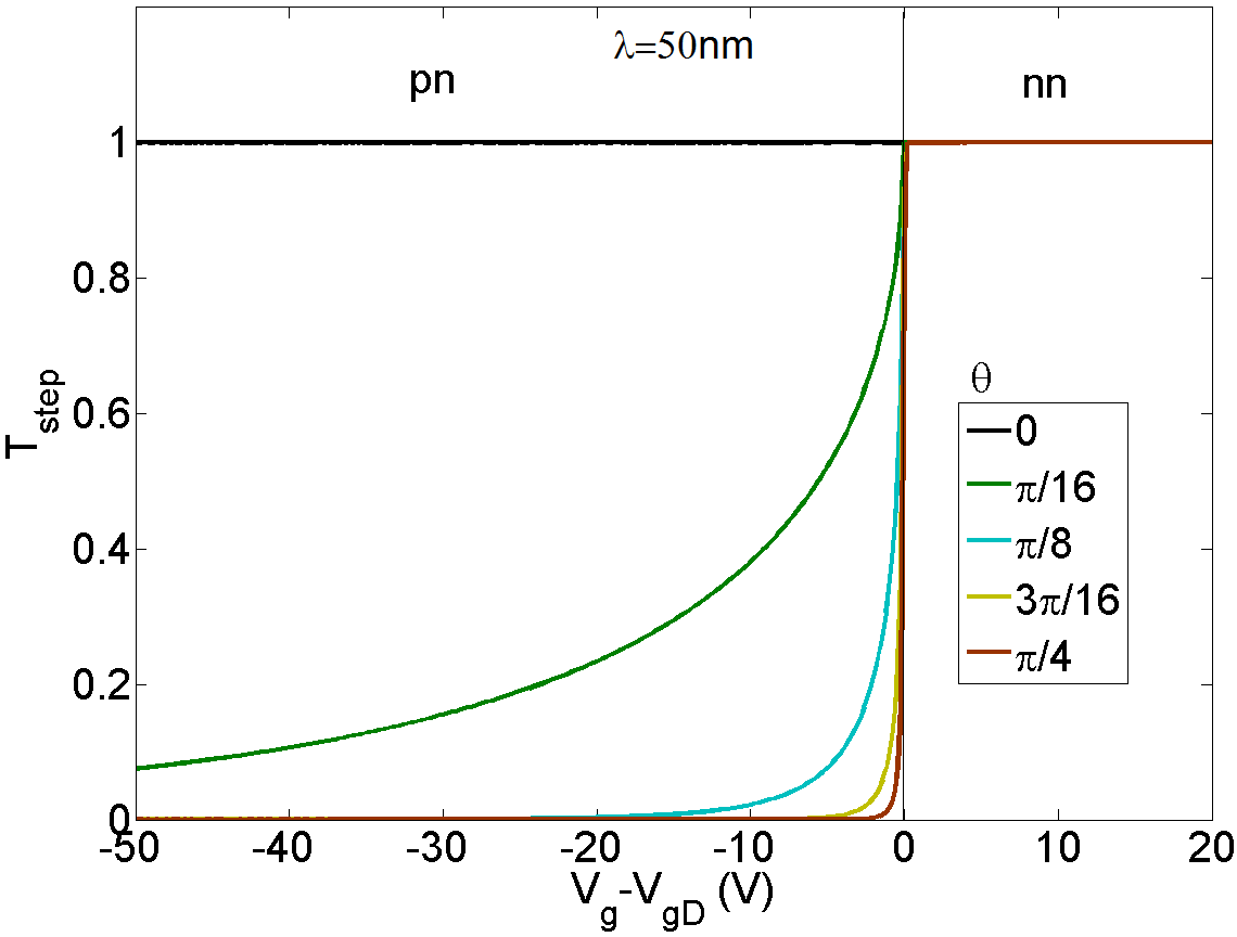
As a complementary information, the dependence of on the effective length of the potential step between the metal-doped graphene and the gate-controlled graphene channel is presented in Fig. 4c. For unipolar juntions, is almost independent of while for the bipolar junction it moderately increases as changes from 2 to 128 nm.
After presentation of the model, next is benchmarking it against experimental measurements in graphene FETs using the transfer length method (TLM) for metal electrodes such as Palladium (Pd), Nickel (Ni) and Titanium (Ti) as shown below.
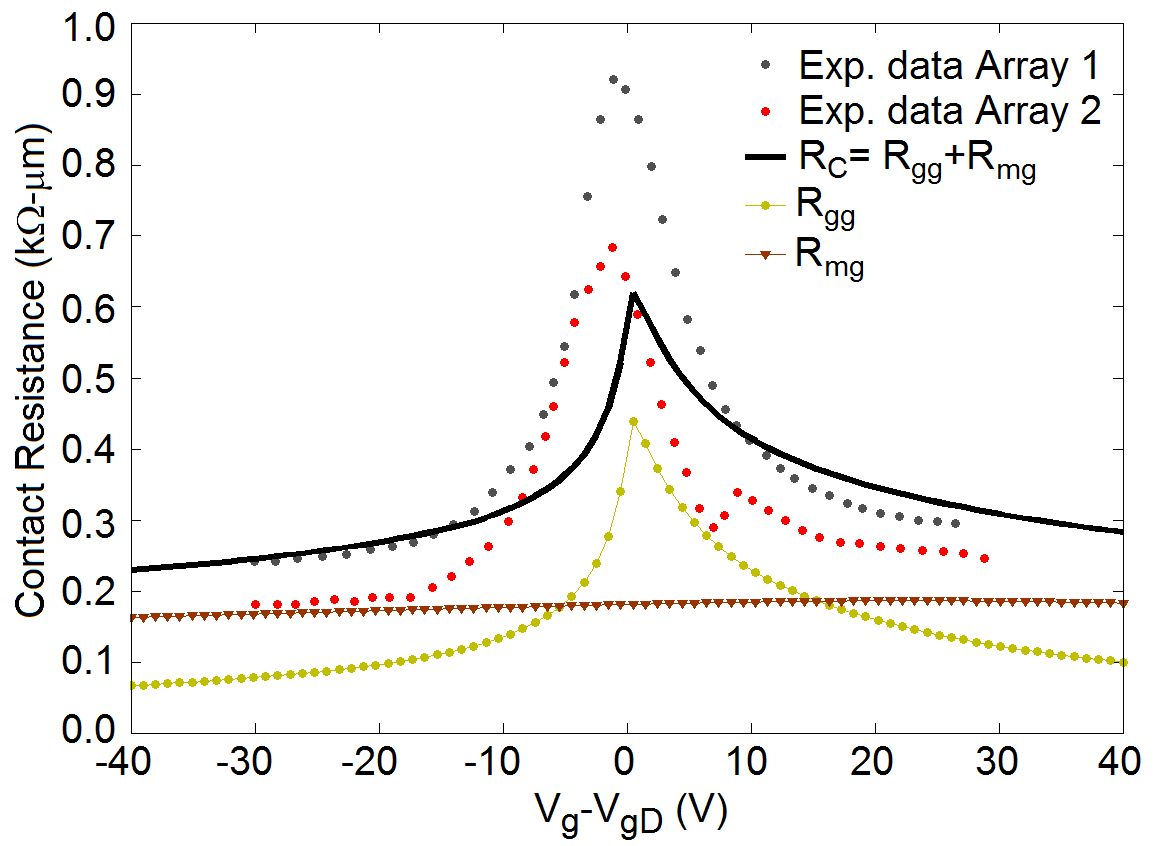
In Fig. 5 we have plotted the data reported by Xia et al. considering Pd as metal electrode. Here the graphene sheet was transferred to SiO2 of 90 nm thickness. Our model reveals that and play a similar role. The absence of a peak in the experimental data at V suggests a large value of , as it has previously been discussed. To match the experimental data we have assumed cm-2, meV, meV and nm. Interestingly we capture the correct value of the Dirac voltage at V and the moderate asymmetry between the left and right branches: being lower for the left branch because of the much better carrier transmission of the unipolar pp junction as compared with the bipolar pn junction (see Fig. 4a).
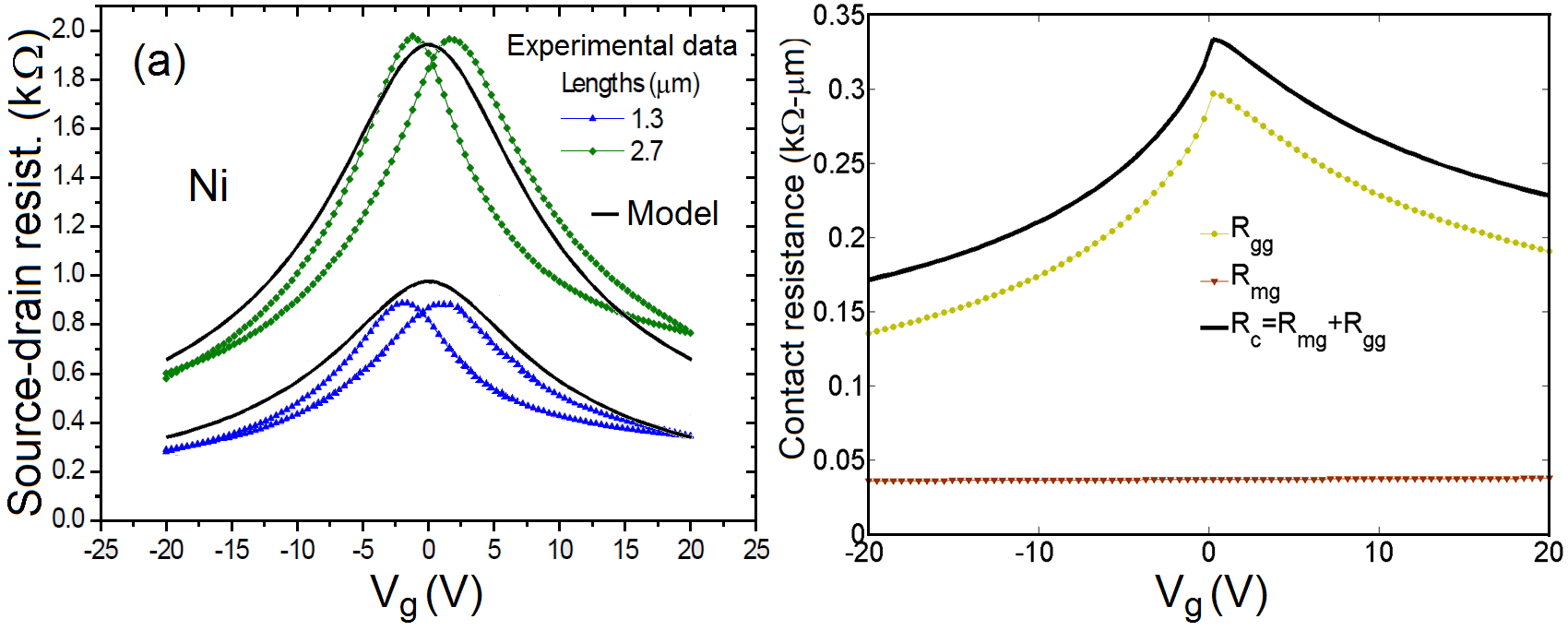
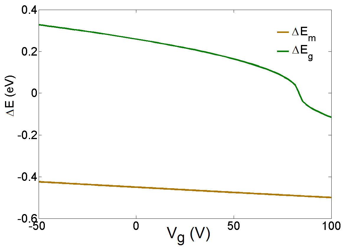
Next, we compare with experimental data of GFETs with Ni as metal electrode (Fig. 6). In this case, the back-gated graphene transistors have been fabricated by photolithography on Si wafers covered by 300 nm of thermal oxide. Graphene grown by chemical vapor deposition (supplier Bluestone Global Tech) was transferred by the standard PMMA method 20 to the substrate and patterned using oxygen plasma. Nickel-contacts have been fabricated using sputter deposition and lift-off technique. The distance between source and drain contacts was 0.6, 0.9, 1.3, 1.7 and 2.7 m for different devices on the chip to allow extraction of by TLM. The channel width was 10m. Finally the devices have been encapsulated by 85 nm of Al2O3 deposited by atomic layer deposition. After some electrical measurements, we report in Fig. 6a the comparison between the experimental data and the usual model of the source to drain resistance given by21:
| (12) |
Here, the channel sheet resistance has been modeled as , with cm2V-1s-1 and cm-2 which were extracted from the experiment, and is the charge sheet concentration in the graphene channel region. In this case we have assumed a possible doping concentration in the graphene channel of cm-2 in order to capture the position of the Dirac voltage. Details of the electrostatic behavior of the Ni-graphene contact can be found in the Supplementary data. For the quasi-static measurements of resistance shown in Fig. 6a hysteretic behavior is observed, which is typical for graphene FETs. This hysteretic behavior occurs mainly because of charge traps generated by adsorbates, typically O2/H2O redox couples, at the graphene/dielectric interface 22, 23. This effect has not been considered in this model. Regarding the contact resistance (Fig. 6b), our model gives values between 150 and 350 -m, which are consistent with the experimental values extracted by TLM for the gate voltages -20, 0 and 20: 220, 400 and 220 -m with correlation coefficient and , respectively. The values of and were determined to be around 4nm and 300meV, respectively, to get values in that range. It is worth metioning that is the dominant part of , which is in contrast with the Pd contact case analyzed before, where and played a similar role.
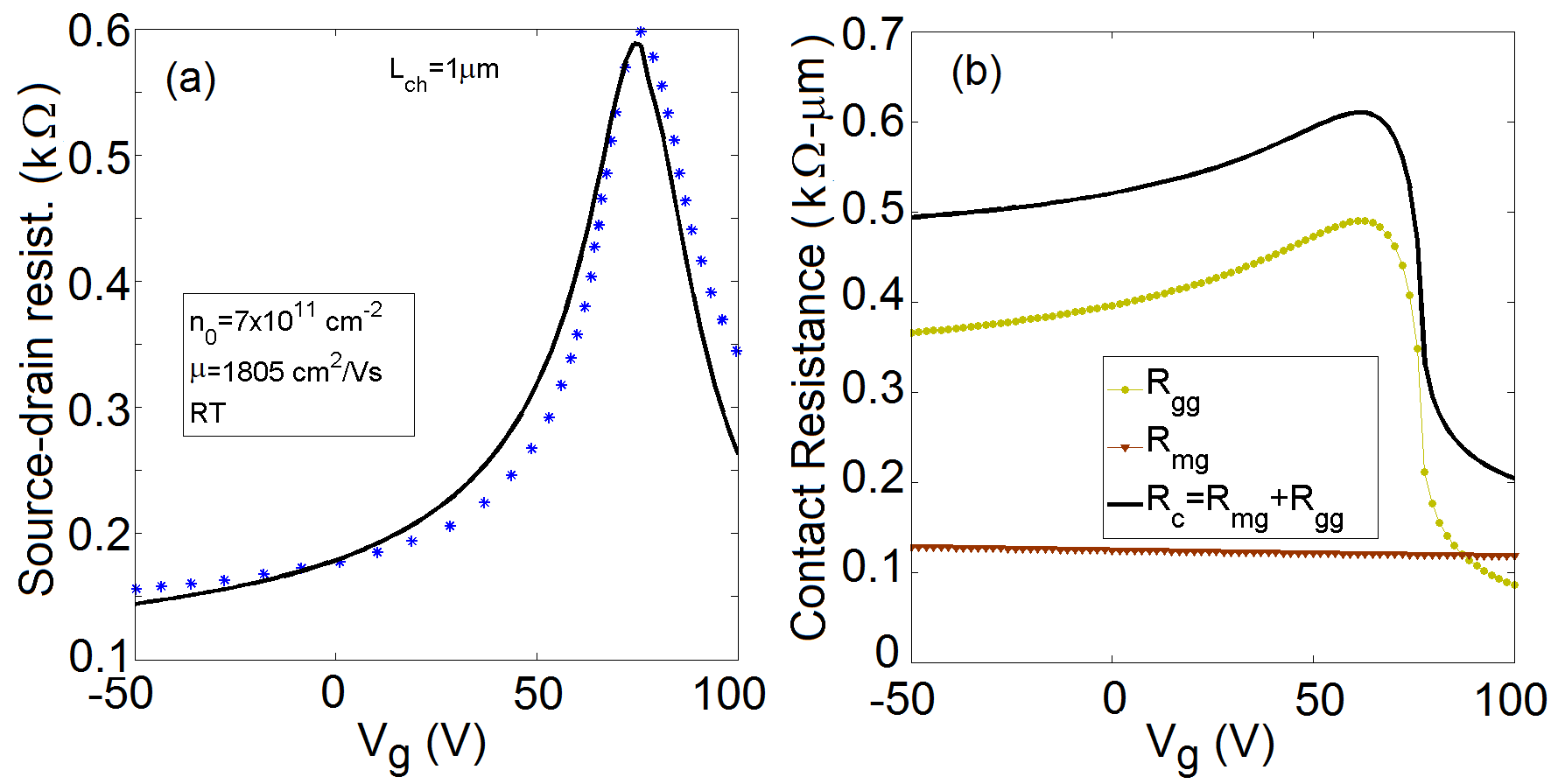
A third comparison was carried out for GFETs with Ti as metal electrode with geometrical parameters: m, m and nm (). Here graphene synthesized by photo-thermal CVD on copper was used to fabricate GFETs 24, 25. Regarding the source-drain resistance, the experimental data are shown in Fig. 7a together with the model prediction on . Similarly to the Ni case, we have considered the following electrical parameters: cm2/Vs, cm-2 as extracted from the experimental data. A chemical doping cm-2 was fed in the model to get the position of the Dirac voltage around 75V in accordance with the observation. Details of the electrostatic behavior of the Ti-graphene contact can be found in the Supplementary data. Using them together with the parameters given in Table I, our model results in the contact resistance shown in Fig. 7b. The calculated agrees well with the extracted values from TLM at gate voltages and V: and -m with correlation coefficient and , respectively. The values of and were determined to be around 50nm and 300meV, respectively, to get values in the mentioned range. Unlike Pd and Ni, in Ti-graphene contact exhibits a huge asymmetry between left and right branches, being lower for the right branch. This asymmetry qualitatively agrees with measurements carried out for Ti and reported by Xia et al.6.
4 Conclusions
In summary, we have developed a model of the gate tunable metal-graphene contact resistance. First of all we have modeled the behavior of the shift Fermi level in both the graphene underneath the metal and graphene in the channel. becomes zero under the metal at gate voltage named as which is controlled by intrinsic electrical parameters like the work function, the capacitive coupling between the metal and the gate and the value of the chemical interaction. In the channel region is zero at gate voltage which is strongly determined by the unintended chemical doping. Once we get in each region, we use a combination of the BTH and the Landauer formula to independently determine the contribution of each component, namely BTH to determine the resistance between metal and the graphene underneath () and Landauer formula for the resistance between graphene under the metal and the graphene in the channel (). Using BTH we have found a simple analytical expression for the specific contact resistivity which elucidates its dependence with the metal-graphene equilibrium distance. Specifically, among the metals considered here, Ni and Ti exhibit the smallest value of at their respectives Dirac voltages . However, given the voltage dependence of and the different value displayed by each metal metal, Cu or Pd could show even a smaller than that for Ni or Ti depending on the applied gate voltage. The calculation of is key to get by means of Transmission Line Method. This resistance shows a peak at . On the other hand, the lateral resistance or , in principle, exhibits two peaks. One of them at and another at . However when a broadening of the graphene states under the metal ( in this work) is considered, the latter peak could disappear. We have also found that is sensitive to the effective length () of the junction potential step, specially when a bipolar pn junction builds up. Depending on the metal electrode and the chemical doping of the graphene channel the two components of could be either similar in magnitude or of very different order. In particular for Pd those two components compete, but for Ni and Ti the lateral resistance is the dominant component.
Our model is in agreement with experimental data for several metals under test. In particular, we have benchmarked the model against experiments using Pd, Ti, and Ni. The proposed model unveils the interplay between different intrinsic and extrinsic factors in determining the contact resistance of graphene-based electronic devices, which should be useful for its optimization.
5 Acknowledgements
We acknowledge support from SAMSUNG within the Global Research Outreach Program. The research leading to these results has received funding from Ministerio of Economía y Competitividad of Spain under the project TEC2012-31330 and from the European Union Seventh Framework Programme under grant agreement n°604391 Graphene Flagship.
6 Supporting Information
6.1 Calculation of the specific contact resistivity
In this section we derive the analytical expression for the specific contact resistivity of the Metal-Graphene junction given by Eq. (5) of the main text, relying on the BTH approach. The starting point is the expression for the tunneling current
| (13) |
where both the subscripts and label the states in the graphene and metal electrodes with energies and , respectively, is the electron spin degeneracy, is the valley degeneracy, and and refer to the tunneling rates for electrons moving from and , respectively. Finally, and are the Fermi occupation factors for the electrons.The tunneling rates are given by the Fermi’s golden rule as
| (14) |
where
| (15) |
are the matrix elements for the transition, with the electron mass in the dipole layer. The terms and represent the graphene and metal electron wavefunctions, respectively. Then, inserting Eq. (14) into Eq. (13), the tunneling current can be expressed as
| (16) |
Considering the graphene with two identical atoms per unit cell, labeled 1 and 2, the wavefunction for wavevector can be written in terms of the basis functions on each atom as . The basis functions have Bloch form, , where is a periodic function and refers to the contact area. These periodic functions are localized around the basis atoms (i.e., as orbitals) of the graphene , and is expected to vary only weakly along the radial coordinate in the graphene. Thus, we assume that and we approximate the radially-dependent term as numerical constants and 13. The -dependence has the usual decaying form , where is the decay constant of the wavefunction in the barrier. The decay constant has the form 13, where is the barrier height in the dipolar layer and is the parallel momentum. For graphene, the latter term is essentially equal to the momentum at the K or K’ points (i.e., so that nm-1 for eV.
Both and have well-known values for graphene in a nearest-neighbor tight-binding approximation 26,
| (17) |
where is the angle of the relative wavevector, the upper sign is for the band extreme at the K point of the Brillouin zone and the lower sign is for the K’ point, with for the conduction band (CB) and -1 for the valence band (VB). On the other hand, the metal electrons can be modeled as free incident and reflected particles for and with a decaying exponential for , namely
| (18) |
where and are the amplitudes of the transmitted and reflected waves, respectively. As usual, the matching conditions and have to be fulfilled, resulting in . Thus, the matrix elements for the transitions of Eq. 15 can be written as
| (19) |
where we have defined . The integral on the right-hand side of Eq. 19 approaches the delta-function when , implying the conservation of in-plane momentum : . Incorporating Eq. 19 into Eq. 16, we get the following expression for the current
| (20) |
The delta Dirac function guarantees that only energy-conserving tunneling processes are possible. From the Fig. (8a) we observe that , with constant and thus The function is , where is a constant of order unity assumed to have no dependence on .
In deriving Eq. 20 we have incorporated both the graphene and metal dispersion relations, namely and , which we have sketched in Fig. (8b) for convenience and . Considering Eq. 20 in the limit of large , , and then the equation for the tunneling current becomes
| (21) |
where we have defined the function . The discrete sums over and are converted to integrals using the recipes and . After some algebra, the tunnel current density becomes
| (22) |
where . The energy difference appearing in the delta-function can be written as,
| (23) |
where with ,. Using the Dirac delta function properties we can write and Eq. 22 becomes
| (24) |
Since we are interested in the specific contact resistivity (i.e ) we have approximated the Fermi levels difference by , where . Given that is fulfilled, we can approximate to find an analytical solution for Eq (24). Thus Eq. (24) can be expressed as
| (25) |
Now integrals of the type
| (26) |
where , have to be resolved for every cone. Thus, the current density takes the form
| (27) |
Finally, an analytical expresssion for the specific contact resistivity as the Eq. (5) in the main text is deduced.
6.2 Effect of the broadening on the contact resistance
The two components of the contact resistance must be modified to take into account the broadening of the states in both graphene under the metal and graphene in the channel, namely;
| (28) |
| (29) |
where and are given by Eqs. (4) and (9) of the main text and the Gauss function is .
6.3 Ni-Graphene junction
Fig. 9(a) shows the shift of the Fermi level respect the Dirac point for the Ni-graphene junction. Important values are V and V defining the crossover between unipolar pp-junction/bipolar pn-junction and bipolar pn-junction/unipolar nn-junction, respectively. The electrical parameters for this simulation have been mentioned in the main text. On the other hand, Fig. 9(b) shows the transmission probability of the Dirac fermions across the potential step for different incidence angles.
6.4 Ti-Graphene junction
Fig. 10(a) shows the shift of the Fermi level respect the Dirac point for the Ti-graphene junction. Important value here is V defining the crossover between bipolar pn-junction/unipolar nn-junction. The electrical parameters for this simulation have been mentioned in the main text. On the other hand, the Fig. 10(b) shows the transmission probability of the Dirac fermions across the potential step for different incidence angles.
References
- 1 Novoselov, K. S.; Geim, A. K.; Morozov, S. V.; Jiang, D.; Zhang, Y.; Dubonos, S. V.; Grigorieva, I. V.; Firsov, A. A. Science 2004, 306, 666-669.
- 2 Schwierz, F. Proc. IEEE 2013, 101, 1567-1584.
- 3 Huard, B.; Stander, N.; Sulpizio, J. A.; Goldhaber-Gordon, D. Phys. Rev. B: Condens. Matter Mater. Phys. 2008, 78, 121402(R).
- 4 Nagashio, K.; Nishimura, T.; Kita, K.; Toriumi, A. IEEE Int. Electron Devices Meet. 2009, 5424297.
- 5 Russo, S.; Craciun, M. F.; Yamamoto, M.; Morpurgo, A. F.; Tarucha, S. Physica E 2010, 42, 677-679.
- 6 Xia, F.; Perebeinos, V.; Lin, Y.-m.; Wu, Y.; Avouris, P. Nat. Nanotechnol. 2011, 6, 179-184.
- 7 Sundaram, R. S.; Steiner, M.; Chiu H-Y.; Engel, M.; Bol, A. A.; Krupke, R.; Burghard, M.; Kern, K.; Avouris, P. Nano Lett. 2011, 11, 3833-3837
- 8 Bardeen, J. Phys. Rev. Lett. 1961, 6, 57-59.
- 9 Tersoff, J.; Hamann, D. R. Phys. Rev. B 1985, 31, 805.
- 10 Cayssol, J.; Huard, B.; Goldhaber-Gordon, D. Phys. Rev. B: Condens. Matter Mater. Phys. 2009 79, 075428.
- 11 Khomyakov, P. A.; Giovannetti, G.; Rusu, P.C.; Brocks, G.; Van den Brink, J.; Kelly, P. J. Phys. Rev. B 2009, 79, 195425.
- 12 Chaves, F. A.; Jiménez, D.; Cummings, A. W.; Roche, S. J. Appl. Phys. 2014, 15, 164513.
- 13 Feenstra, R. M.; Jena, D.; Gu, G. J. Appl. Phys. 2012, 111, 043711
- 14 Ni, Z. H.; Wang, H. M.; Luo, Z. Q.; Wang, Y. Y.; Yu, T.; Wu, Y. H.; Shen, Z. X. J. Raman Spectrosc. 2010, 41, 479-483.
- 15 Schroder, D. K. Semiconductor Material and Device Characterization, 3rd Ed.; John Wiley and Sons, Inc.: Hoboken, NJ, 2006.
- 16 Léonard, F.; Talin, A. A. Nature Nanotech. 2011, 6, 773.
- 17 Reeves, G. K.; Harrison, H. B. IEEE Electron Dev. Lett. 1982, 3, 111-113.
- 18 Nagashio, K.; Nishimura, T.; Kita, K.; Toriumi, A. Appl. Phys. Lett. 2010, 97, 143514.
- 19 Berdebes, D.; Low, T.; Sui, Y.; Appenzeller, J.; Lundstrom, M. IEEE Trans. Electron Dev. 2011, 58, 3925-3932.
- 20 Li, X.; Cai, W.; An, J.; Kim, S.; Nah, J.; Yang, D.; Piner, R.; Velamakanni, A.; Jung, I.; Tutuc, E.; Banerjee, S. K.; Colombo, L.; Ruoff, R. S. Science 2009, 324(5932), 1312-1314.
- 21 Kim, S.; Nah, J.; Jo, I.; Shahrjerdi, D.; Colombo, L.; Yao, Z.; Tutuc, E.; Banerjee, S. K. Appl. Phys. Lett. 2009, 94, 062107.
- 22 Xu, H.; Chen, Y.; Zhang, J.; Zhang, H. Small 2012, 8(18), 2833-2840.
- 23 Lee, Y. G.; Kang, C. G.; Cho, C.; Kim, Y.; Hwang, H. J.; Lee, B. H. Carbon 2013, 60, 453-460.
- 24 Riikonen, J.; Kim, W.; Li, C.; Svensk, O.; Arpiainen, S.; Lipsanen, H. Carbon 2013, 62, 43-50.
- 25 Kim, W.; Riikonen, J.; Li, C.; Lipsanen, H. Nanotechnology 2013, 24, 395202.
- 26 A.H. Castro, F. Guinea, N. M. R. Peres, K. S. Novoselov and K. Geim, Rev. Mod. Phys. 81, 109-160 (2009)