Transport through graphene-like flakes with intrinsic spin orbit interactions
Abstract
It has been shown recently [J. L. Lado et al., Phys. Rev. Lett. 113, 027203 (2014)] that edge magnetic moments in graphene-like nanoribbons are strongly influenced by the intrinsic spin-orbit interaction. Due to this interaction an anisotropy comes about which makes the in-plane arrangement of magnetic moments energetically more favorable than that corresponding to the out-of-plane configuration. In this paper we raise both the edge magnetism problem as well as differential conductance and shot noise Fano factor issues, in the context of finite-size flakes within the Coulomb blockade (CB) transport regime. Our findings elucidate the following problems: (i) modification of the CB diamonds by the appearance of the in-plane magnetic moments, (ii) modification of the CB diamonds by intrinsic spin-orbit interaction.
pacs:
73.22.Pr, 72.80.Vp, 73.63.Kv, 73.23.HkI Introduction
Graphene-like nanostructures – including silicene Guzman2007 , germanene Cahangirov2009 and hypothetically also stanene (two-dimensional tin) Liu2011 , aluminene Kamal2015 and others – constitute a particularly challenging class of materials potentially important for future applications in nanoelectronics and spintronics. On the one hand, the great interest in these materials results from many fascinating properties of graphene Geim2007 , which have been discovered and reported in the last decade. It is believed that these new nanomaterials akin to graphene as regards the honeycomb atomic structure and possibly also the Dirac fermion features, will also share well-known graphene’s superlatives concerning mechanical, optical, electrical, magnetic and thermal properties. NetoRMP09 Due to the nonequivalence of the involved sublattices (buckling) and the possibility to engineer an energy band gap, Zandvliet2014 the new nanostructures, in contrast to graphene, may prove to be useful for realization of the field effect transistor. Tao15
Some other interesting properties of these two-dimensional materials follow from internal spin-orbit interaction. Ezawa In the bulk (two-dimensional) limit, this interaction opens a gap at the Fermi level in the electronic spectrum of the corresponding Dirac fermions. This gap leads to the spin Hall insulator phase.Kane2005 Moreover, the induced gap can be tuned by an external electric field oriented perpendicularly to the system’s plane.Dyrdal ; Drummond12 Unfortunately, the intrinsic spin-orbit interaction is rather small in these materials, therefore the gap is hardly resolved in experiments. Additionally, the spin-orbit coupling can give rise to an in-plane magnetic anisotropy, so that the edge magnetic moments induced by Coulomb interactions become oriented in the layer plane.Lado2014
The electronic spectrum, and especially the energy gaps in the spectrum, can also be controlled by other means. It is well known that a key factor responsible for opening energy gaps is the reduced geometry (confinement effect). This, in turn, has a significant influence on transport properties, as shown for instance in the case of long silicene nanoribbons Lou2009 ; Zhang2010 ; Lopez2013 ; Zberecki and graphene quantum dots.Weymann2012 Remarkable impact on the electronic structure is also due to the edges, e.g. zigzag vs. armchair ones. Moreover, electron correlations, especially of Hubbard-type, also play a role in the formation of spin-dependent electronic states.
In this paper we study the effects of spin-orbit interaction on electronic and transport properties of small graphene-like flakes, in which size quantization in both directions occurs. The corresponding electronic spectrum of such graphene-like quantum dots (GLQDs) is then discrete. To model the system, apart from the on-site Coulomb interaction (of Hubbard type), one then also has to account for the Coulomb blockade effects, especially when the coupling of the dot to external leads is relatively weak, as considered in this work. With the aid of the exact diagonalization, we first find the eigenstates and eigenvalues of isolated GLQD, which are then used to determine the transport characteristics by using the real-time diagrammatic technique in the lowest order perturbation expansion with respect to the coupling to external leads. diagrams ; thielmann ; weymannPRB08 In particular, we calculate the differential conductance as well as the shot noise in both the linear and nonlinear response regimes. Since the conductance and Fano factor provide information about the electronic spectrum of the system, and the electronic states are modified by the Coulomb and spin-orbit interactions, the calculated transport characteristics vs gate and transport voltages allow us to draw some conclusions on these interactions.
The format of the paper is as follows. In Sec. II the Hamiltonian (Sec. II.1) and electronic structure (Sec. II.2) of GLQD are presented. The importance of the intrinsic spin-orbit interaction and its effect on the appearance of the in-plane anisotropy is emphasized, and the results on edge magnetism and energy spectra of an isolated GLQD are presented. Transport properties are considered in Sec. III. The effective Hamiltonian and method for studying transport properties are described in Secs. III.1 and III.2, respectively, while transport characteristics are analyzed in Sec. III.3. Finally, Sec. IV summarizes the main findings.
II Electronic properties
In the following we analyze the electronic properties of an isolated quantum dot of graphene-like materials. We first present the Hamiltonian of GLQD in the mean field approximation. Then, by means of exact diagonalization, we find the eigenstates and eigenvalues of the dot and analyze its electronic and spin properties.
II.1 Hamiltonian
The system under consideration is described by a tight-binding Hamiltonian which also contains, apart from the usual hopping term, the intrinsic spin-orbit and the Hubbard correlation terms. The latter is treated within the mean-field approximation. Thus, the Hamiltonian can be written as
| (1) |
where the first term is given by
| (2) |
while the second term takes into account the Coulomb correlations in the mean-field approximation and has the form
| (3) | |||||
Here, are the corresponding occupation operators, , while and , with () being the creation (annihilation) operator of spin- -electrons at a lattice point . The angle brackets stand here for the expectation values calculated with respect to the ground state of the Hamiltonian . Moreover, is the Hubbard parameter of the on-site repulsion, denotes the intrinsic spin-orbit parameter, whereas and are the hopping integrals and the Haldane factors between nearest neighbor and next nearest neighbor sites, respectively. For a pair of next nearest sites, and , with a common nearest neighbor , . HaldanePRL88 ; Kane2005 For simplicity, the hopping integrals are assumed to be nonzero only for nearest neighbors, and the corresponding hopping parameter is used as the energy unit (e.g. 2.7, 1.5, 1.4, 1.3 eV for graphene, silicene, germanene and stanene [Lado2014, ], respectively).
It is noteworthy that the correlation part of the Hamiltonian, , comes from the full Hartree-Fock decoupling of the Hubbard Hamiltonian. Usually only the first spin-diagonal part of Eq. (3) is taken into account. Fernandez07 ; Weymann2012 ; SK1214 ; Szal15 However, in the present anisotropic case the magnetization direction may be arbitrary, so the spin mixing term must not be skipped. Similar Hamiltonians, in other contexts, were studied i.a. in Refs. [Rhim2009, ; Lado2014a, ].
In numerical calculations the Coulomb on-site repulsion is assumed to be (cf. Ref. [Lado2014, ]). The expectation values of the relevant occupation numbers, , have been computed self-consistently by summing up the squared eigenvectors corresponding to the eigenvalues not greater than the Fermi energy. Furthermore, for the out-of-plane and in-plane configurations the following order parameters come into play: and , where is the Bohr magneton.
II.2 Electronic and spin structure
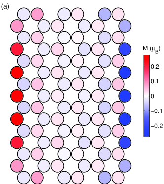
To exemplify our results we consider a relatively small zigzag-type rectangular GLQD containing atoms, see Fig. 1(a). The model system is a honeycomb structure as that of graphene, but in contrast to graphene, now the sublattices and are vertically shifted with respect to each other by the distance of the order of 0.5 Å. Cahangirov2009 Incidentally, we have checked by performing additional computations for some longer systems, that this model is large enough to yield correct magnetic moments at its mid-length. The buckling of the considered graphene-like flake is closely related with the intrinsic spin orbit interaction – if buckling is negligible, then , and one obtains the case of graphene.
Since the electronic and magnetic properties of the considered GLQD depend greatly on both the on-site Coulomb correlations and spin-orbit interactions, to elucidate the role of those interactions, in the following we present and discuss results for the case of and , as well as and . As shown below, finite on-site Coulomb correlations are responsible for magnetic moments at individual atoms that form at the edges (edge magnetism). On the other hand, the spin-orbit interaction determines the magnetization configuration and its anisotropy.
II.2.1 Absence of spin-orbit interaction
The distribution of magnetic moments at individual atoms of the considered flake in the absence of spin-orbit interaction and for is shown in Fig. 1(a). In the case of , the magnetization is isotropic. It is readily seen that magnetic moments have relatively high values (roughly 0.3 ) at the zigzag edges, except at atoms located close to the armchair edges. Moreover, while atoms belonging to one sublattice are magnetized in one direction, the magnetization of atoms from the other sublattice is opposite, see Fig. 1(a). This antiparallel magnetic configuration has got a lower energy than the parallel one.
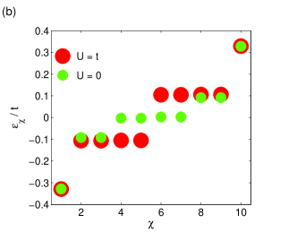
The eigenenergies of the GLQD Hamiltonian are shown in Fig. 1(b) in the case of both finite and . This figure presents discrete energy levels around the Fermi level (defined by the charge neutrality point, ), with ranging from 1 to 10. These energy levels will be later used for studying the transport properties. Due to the Hubbard correlations, an energy gap develops, see the large points in Fig. 1(b). However, if the correlations disappear, [see the small points in Fig. 1(b)], the energy gap closes at the charge neutrality point, and degenerate energy states appear at the Fermi energy.
II.2.2 Finite spin-orbit interaction

The situation changes when the spin-orbit interactions are present, since now magnetic anisotropy develops. As a result, magnetic configurations corresponding to the in-plane and the out-of-plane orientations differ from each other. The calculations show that energetically more favorable is the configuration with the in-plane easy axis. The obtained magnetization profile is shown Fig. 2(a). In comparison with Fig. 1(a), the magnitude of magnetic moments is now slightly diminished. Moreover, similarly as in the case of , the direction of magnetic moments is opposite for atoms belonging to different sublattices. The corresponding eigenenergies around the Fermi level are shown in Fig. 2(b). One can see that now there appears a small energy gap of purely spin-orbit origin when [the small points in Fig. 2(b)]. The energy gap gets pronouncedly increased due to an extra magnetic contribution for , see the large points in Fig. 2(b).
Figures 1 and 2 show that the dominant contribution to the band gap is magnetic in nature and results from finite Coulomb correlations. The intrinsic spin-orbit contribution is competitive with the magnetic one and, consequently, the net energy gap gets reduced while increasing the spin-orbit parameter , cf. Figs. 1(b) and 2(b). Interestingly, a similar tendency can also be deduced from the results presented in Ref. [EzawaPRL12, ] for the out-of-plane configuration. Moreover, the aforementioned behavior resembles to some extent the competition between a vertical electric field and the intrinsic spin-orbit interaction, as reported recently. Drummond12 ; EzawaPRL12 ; DrummondPRB13
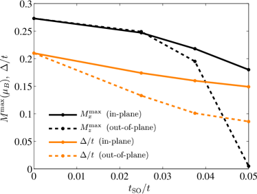
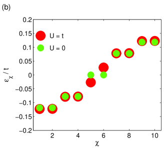
A more detailed analysis of the effect of the intrinsic spin-orbit coupling on the maximum (mid-length) magnetic moment () and the corresponding energy gap () is depicted in Fig. 3. The data were calculated for and are shown for both in-plane and out-of-plane configurations. As can be seen in the figure, both and decrease with increasing the spin-orbit coupling parameter . As mentioned above, this decrease is related with competition between spin-orbit and magnetic contributions. For larger values of the spin-orbit coupling, these two quantities are even more strongly affected in the unstable out-of-plane configuration, see Fig. 3.
We would like to note that for the considered rectangular graphene-like flakes with both zigzag and armchair edges, our numerical results show that noticeable magnetic moments can only appear on edges of the former type. Moreover, due to the spin-orbit interaction these moments are oriented in the plane of the flakes. The question which now arises is whether these observations are more general and also hold for other shapes of the flakes. This problem in the absence of spin-orbit interaction was considered e.g. in Refs. [Weymann2012, ; Kikutake, ; Rakyta, ], from which follows that localized edge magnetic moments exist mainly on zigzag-like fragments of an arbitrary boundary. To address this issue in the presence of spin orbit interaction in the Appendix we consider a flake of circular shape exhibiting some irregularities. Our results suggest that the above observation is indeed applicable for more general shapes of graphene-like flakes. Moreover, we also show that the magnetic moments are oriented in the plane of the flake, similarly to the case of rectangular flakes.
III Transport properties
In this section we focus on the analysis of transport properties of GLQD attached to external electrodes. We assume that the coupling between the dot and external leads is relatively weak, so transport occurs mainly due to sequential tunneling processes. To determine transport characteristics, we employ the real-time diagrammatic technique in the lowest order of perturbation expansion with respect to the coupling strength between GLQD and the leads.
III.1 Effective Hamiltonian
From exact diagonalization of the GLQD’s Hamiltonian (1) we obtain the eigenvalues and eigenstates . Since in our analysis we are interested in the low bias voltage regime, in calculations we will consider only limited number of eigenstates with eigenvalues close to the charge neutrality point. The Hamiltonian of the isolated GLQD can be written as
| (4) |
where is the creation operator for an electron of energy . Note that in general the states are linear combinations of both spin-up and spin-down states when the quantization axis is normal to the system’s plane. The charging energy of the graphene-like quantum dot is denoted by , , while denotes the number of electrons in the electrically neutral dot.
The Hamiltonian of electrodes, in turn, takes the form
| (5) |
and models the leads as reservoirs of noninteracting quasi-particles. Here, is the creation operator for a spin- electron with wave vector in the bottom () or top () lead, while denotes the corresponding energy.
The tunneling processes between the GLQD and the leads can be described by the following tunneling Hamiltonian
| (6) |
where is the hopping matrix element between the dot and the lead , which is assumed to be momentum and spin independent. The coefficient is defined as
| (7) |
where means that the summation is over the -th row of atoms counted from bottom () or top side of the flake, which is attached to the electrodes. If one includes all the atoms, then . The effective broadening of the GLQD’s levels can be described by
| (8) |
with being the density of states of lead and .
In calculations we consider the coupling to the first row of atoms next to the contacts, that is , and assume that the tunnel matrix elements for are negligible. This assumption is justifiable since tunnel matrix elements depend exponentially on the distance, and the coupling to next rows of atoms is expected to change the GLQD level widths only insignificantly. We thus assume (): . The charging energy of the graphene-like quantum dot is estimated to be (see Ref. [Ma13, ] for details concerning graphene QD). Moreover, in calculations we restrict ourselves to the low energy regime and take into account states of GLQD around the Fermi level. Weymann2012
III.2 Method
To determine the transport characteristics we make use of the diagrammatic technique in real time. diagrams ; thielmann Within this approach, one performs a systematic perturbation expansion of the reduced density matrix and relevant operators with respect to the tunneling processes between the nanostructure and the leads. In the following analysis we focus on the weak coupling regime and assume that the main contribution to the conductance is captured by the lowest-order tunneling processes, where electrons tunnel sequentially, one by one, through the junction. In the considered case the density matrix is diagonal and its elements, which directly correspond to the occupation probabilities of respective GLQD states , can be found from appropriate kinetic equation. diagrams In the steady state, one has diagrams ; thielmann
| (9) |
together with normalization condition, . Here, is the self-energy matrix whose elements, , describe transitions between respective states and . These matrix elements can be found using the respective diagrammatic rules diagrams ; thielmann ; weymannPRB08 and are given by , with
for and . Here, is the Fermi-Dirac distribution function and denotes the electrochemical potential of lead . The current flowing through the system can be found from diagrams ; thielmann
| (10) |
where the elements are essentially given by but this time they take into account the number of electrons transferred through the system. diagrams ; thielmann In addition, to gain more detailed understanding of transport properties, we also study the behavior of the Fano factor, , which measures the deviation of the zero-frequency shot noise from the Poissonian shot noise given by, . blanterPR00 The formula for the calculation of shot noise using the diagrammatic technique can be found in Ref. [thielmann, ].
III.3 Numerical results
Using the above described formalism we have computed the differential conductance density plots, i.e. the differential conductance vs. bias voltage and gate voltage (effectively the position of the electronic spectrum of GLQD denoted by ), as well as the density plots of the corresponding shot noise Fano factor. In the following we focus mainly on analyzing the effects of the on-site Coulomb interaction (edge magnetism) and spin-orbit coupling on transport characteristics. To analyze the role of edge magnetism, we consider first the situation with zero spin-orbit coupling, .
III.3.1 No spin-orbit interaction
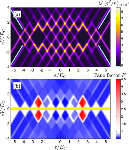
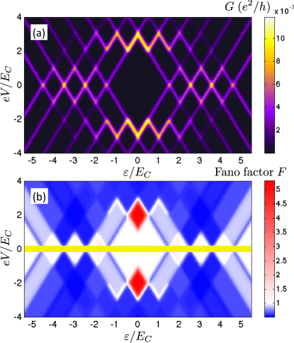
The numerical results on the differential conductance and Fano factor for and are presented in Figs. 4 and 5, respectively. In both cases the spin-orbit interaction was assumed to be equal to zero, . Since the Coulomb interaction leads to edge magnetic moments, the latter figure also illustrates effectively the impact of the edge magnetism on both the Coulomb blockade (conductance) and the Fano factor spectra.
The bias and gate voltage dependence of the differential conductance in the case of is presented in Fig. 4(a). This figure shows the stability diagram of the device, with Coulomb diamonds visible at low bias voltage. In diamonds the current through the system is suppressed by the charging energy and only thermally-activated or higher-order tunneling events are possible. The rate of sequential processes increases once the voltage approaches a threshold voltage, leading to a step in the current and associated peak in the differential conductance. Next steps occur with further increasing the bias voltage, leading to additional lines in , see Fig. 4(a). Since from the size of Coulomb diamonds one can extract information on the relevant energy scales, let us discuss it in more detail.
In the case of , there are four roughly degenerate states of in an isolated dot, see Fig. 1. The energy difference between these dot levels is resolved neither in Fig. 1(b) nor in Fig. 4(a). These four discrete states are responsible for the three central diamonds visible in Fig. 4(a), which are equal in size. The middle diamond refers to the charge neutrality point, when the two discrete zero-energy levels out of the four ones are occupied by electrons and the dot is then electrically neutral. Considering in Fig. 4 (and also in other figures) as an effective gate voltage, the next discrete state becomes occupied when the energy shift due to the gate voltage is equal to . The dot becomes then charged with one excess electron. In turn, the fourth discrete level becomes populated when the energy shift due to the gate voltage is equal to , so that two excess electrons can reside on the dot for . When the gate voltage increases further, then the third excess electron can enter the dot, and this electron will occupy one of the two levels of higher (positive) energy [cf. Fig. 1(b)]. The additional shift due to the gate voltage must be now larger, as it is equal to the charging energy plus the corresponding level spacing. This corresponds to the first large diamond on the positive energy side of Fig. 4(a). The next diamond is of the same size as the central one since the corresponding gate shift is again equal to . Similar scenario also holds when the gate voltage changes sign, except that now the number of excess electrons becomes negative. Since the energy spectrum is symmetrical around due to the particle-hole symmetry, the whole spectrum in Fig. 4(a) is also symmetrical with respect to the sign change of .
The corresponding Fano factor is shown in Fig. 4(b). When , the shot noise is Poissonian, while for () the noise is super-Poissonian (sub-Poissonian). To facilitate identification of different behavior of the Fano factor, figures presenting density plots of are plotted in appropriately tuned scale. Moreover, because the Fano factor is divergent when , this transport region is covered by a yellow stripe. As can be seen in Fig. 4(b), the shot noise is predominantly super-Poissonian, , in the Coulomb blockade regions (diamonds), where the sequential transport is suppressed by the Coulomb interaction. Only in small parts of the diamonds the noise is close to Poissonian. On the other hand, beyond the Coulomb blockade regions, the shot noise is sub-Poissonian, , which is typical for Coulomb-correlated transport. We note that transport in the Coulomb blockade regime may not be described quite well by the first-order (sequential) processes, and to describe it more accurately, one would need to go beyond the sequential tunneling approximation and include also cotunneling processes. cotunneling Nevertheless, since in our considerations we assume a very weak coupling to external leads, our results can still be considered as qualitatively sound.
We note that there is another interesting feature visible in Fig. 4, which is associated with negative values of the differential conductance that develop in some transport regions. In fact, the most pronounced negative differential conductance can be seen when , emphasized in Fig. 4(a) with the cyan (bright) stripes. This effect occurs when discrete energy levels of GLQD are coupled to the leads with considerably different strength and the difference between the couplings occurs for consecutive levels, for which the level spacing is much larger than thermal energy. This happens in the case when , therefore only in this situation we observe the effect of negative differential conductance. More specifically, for e.g. , with increasing the bias voltage, the first step occurs in the current when the electrons tunnel first through more strongly coupled level. However, with further increase of the bias voltage, the weakly coupled level becomes occupied and the current drops, giving rise to corresponding negative differential conductance, see Fig. 4(a).
When the Hubbard parameter is nonzero, the electronic structure of the dot is strongly modified, as shown in Fig. 1(b), and there are no zero-energy states. Instead, there are four almost degenerate levels of a finite positive (and negative) energy. Accordingly, the conductance spectrum shown in Fig. 5(a) is now greatly changed. The central diamond (corresponding to the charge neutral dot) is much larger, as the gate shift for the dot to be charged with one excess electron involves both the charging energy and the energy of the discrete level. Further diamonds are equal since they correspond to populating next levels from the set of four degenerate levels, and therefore their size is determined by only. The corresponding Fano factor is presented in Fig. 5(b). As before, the shot noise is generally super-Poissonian (or close to Poissonian) in the Coulomb blockade regions and sub-Poissonian outside these regions. One should also note that now the largest Fano factor is observed in the central diamond around , which is then very close to (or slightly above) unity, while in the case of super-Poissonian shot noise was mainly present in two largest Coulomb diamonds.
By comparing Fig. 4 and Fig. 5, one can conclude that the key impact of the edge magnetism on the conductance spectra is the appearance of energy gap and the associated enlarged central diamond (blockade region). Moreover, if there are no magnetic moments (), the conductance spectrum is generally more complex than that for . It is because the inter-level spacings in the vicinity of the charge neutrality point are then much smaller than those for (see Fig. 1) and, consequently, the depicted spectra are more poorly resolved. Moreover, there are then also small regions where the differential conductance becomes negative, which follows from different couplings of particular discrete levels to the electrodes.
III.3.2 The role of spin-orbit interaction
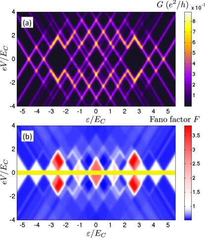
When the spin-orbit interaction is included, the electronic structure of the dot becomes modified. First, for there are then no zero energy states. As shown in Fig. 2(b), the spin-orbit interaction lifts partially the degeneracy and two states are shifted up in energy, while the other two states are shifted down. Accordingly, the central diamond in the conductance spectrum [see Fig. 6(a)] is now larger than the neighboring ones, contrary to the corresponding situation with no spin-orbit interaction [see Fig. 4(a)], where the central blockade diamond is of the same size as the adjacent ones.
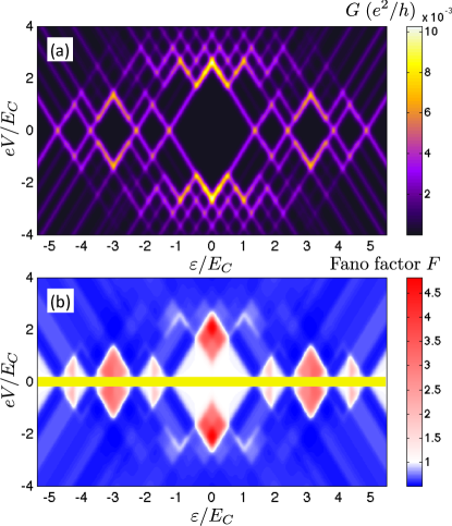
When is nonzero, the electronic structure is qualitatively similar to that for , except that the central gap in the spectrum (the gap between the first pairs of states with positive and negative energy) becomes increased, see Fig. 2(b). This significantly changes the conductance spectra, as can be seen in Fig. 7. Consequently, the central Coulomb blockade diamond is large, while the next one is determined only by the charging energy , and is therefore much smaller. The third Coulomb blockade diamond is only slightly larger than the second one, as it is determined by the charging energy and a small shift of the third energy level relative to the first two ones. As before, the spectrum is symmetric with respect to the particle-hole symmetry point, corresponding to . Interestingly, it turns out that the complexity of the spectra gets enhanced with the increasing parameter. The reason is that magnetic moments get then reduced, and the energy level separations become smaller and smaller.
The corresponding Fano factor is shown in Fig. 6(b) in the case of and in Fig. 7(b) for . As before, the shot noise is generally Poissonian or super-Poissonian in the blockade regions and sub-Poissonian out of these regions. However, a closer look reveals certain differences as compared to the case of , which are most pronounced in the Coulomb blockade regime. In the case of finite spin-orbit interaction, the Fano factor takes the largest values in the central Coulomb diamond, irrespective of the value of . This is associated with the fact that there is an energy gap in the spectrum around zero energy for both finite and zero , cf. Fig. 2(b). For finite , super-Poissonian shot noise can be also found in other Coulomb diamonds, see Figs. 6(b) and 7(b). Moreover, out of the Coulomb blockade regime, the Fano factor is now always much below the Poissonian value, which is contrary to the case of , for which the shot noise is larger, though still .
IV Concluding remarks
In this paper we have addressed the problem of magnetic and transport properties of quantum dots made of graphene-like materials. First, by using exact diagonalization, the intrinsic spin-orbit interaction was shown to have a strong impact on the edge magnetic moments of the dots. In the ground state configuration, these edge magnetic moments in the presence of intrinsic spin-orbit interaction are oriented in the systems’s plane, while states with perpendicular moments correspond to a higher energy. Second, both spin-orbit and on-site Coulomb interactions were found to contribute to the overall energy gap at the Fermi level of an isolated dot. Third, the modification of the electronic spectrum by these interactions was shown to have significant impact on the transport properties of the graphene-like dot.
By employing the real-time diagrammatic technique, we have also studied the behavior of the differential conductance and the Fano factor as a function of bias and gate voltages. The graphene-like quantum dot was assumed to be weakly coupled to external leads and transport was calculated by including the sequential tunneling processes. The stability diagrams and the Fano factor spectra have been shown to include some information on the edge magnetism (on-site Coulomb interaction) and on the intrinsic spin-orbit coupling. More specifically, both these interactions remove the degeneracy of zero energy states and therefore contribute to the increased size of central Coulomb blockade diamonds. The size of the diamond is determined by the charging energy and the energy separation of two successive relevant energy levels. However, if some diamonds are equal in size, the corresponding differential conductances might be different. This is because, in general, different discrete energy levels are coupled to the leads with different strengths. In certain cases, this may give rise to negative differential conductance.
In summary, the main result of this study is a detailed analysis of the combined effect of the intrinsic spin orbit interaction and the resulting in-plane edge magnetization on the Coulomb blockade spectra. We have shown that the Coulomb blockade spectra give important bits of information on the involved edge magnetism and its easy plane. On the one hand, our calculations have shown that protected edge states do not appear in the case of small graphene-like flakes with the in-plane edge magnetization. This is in accordance with the energy band structure results reported for infinitely long ribbons, Lado2014 which clearly show that no crossing energy levels appear in the band gap in that case (in contrast to the out-of-plane case). On the other hand, we have demonstrated that the in-plane magnetization, as well as the corresponding energy gap is relatively robust against the intrinsic spin orbit interaction. From the perspective of potential spintronic applications the first fact is rather disappointing, but the second one is positive.
Acknowledgements.
This project was supported by the Polish National Science Centre from funds awarded through the decision No. DEC-2013/10/M/ST3/00488.*
Appendix A Effect of edge irregularities
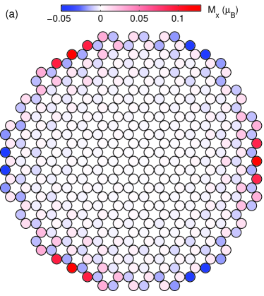
It is important to test whether the findings presented in the main text are still valid for other less simple geometries than those of rectangular flakes. To do this we consider a graphene-like flake of a nanodisk (circular) shape, large enough to contain both zigzag and armchair type arrangements of edge atoms, see Fig. 8(a). The corresponding spin and energy structure calculated for =0.025 and is presented in Figs. 8(a) and (b), respectively. It can be clearly seen that indeed magnetic moments are located at zigzag-type fragments of the circumference. Moreover, the magnetic moments calculated for other values show that the edge magnetic moments decrease with increasing and the in-plane magnetic configuration is always energetically more favorable than the out-of-plane one. Similarly to the case of rectangular flakes, also the nanodisk’s edge magnetic moments of the in-plane configuration are greater than those corresponding to the (unstable) out-of-plane configuration.
All this indicates that the effects described in the main part of the paper are relatively resistant to structural irregularities and shape of the flake’s boundary. The only difference between the results in the case of rectangular and circular flakes is that the latter magnetic configuration is ferrimagnetic rather than antiferromagnetic, with magnetic moments reduced by a few tens of percent. This difference results from the increased imbalance of the A and B sublattices, as well as from short lengths of the zigzag-type edge fragments in the nanodisk case.
As concerns the Coulomb blockade stability diagrams, they strictly reflect the underlying energy spectra. Similarly as it was done in the case of rectangular flakes discussed in the main text, from the size of the Coulomb diamonds one can again extract some information about the intrinsic parameters of the flake.
References
- (1) G.G. Guzmán-Verri, L.C. Lew Yan Voon, Phys. Rev. B 76, 075131 (2007).
- (2) S. Cahangirov, M. Topsakal, E. Akturk, H. Sahin, S. Ciraci, Phys.Rev. Lett. 102, 236804 (2009).
- (3) Cheng-Cheng Liu, Hua Jiang, and Yugui Yao, Phys. Rev. B 84, 195430 (2011).
- (4) C. Kamal, A. Chakrabarti, and M. Ezawa, cond-mat/arXiv:1502.05874v1
- (5) A. K. Geim and K. S. Novoselov, Nature Mater. 6, 183 (2007).
- (6) A. H. Castro Neto, F. Guinea, N. M. R. Peres, K. S. Novoselov, and A. K. Geim, Rev. Mod. Phys. 81, 109 (2009).
- (7) H. J. W. Zandvliet, Nano Today 9, 691694 (2014).
- (8) Li Tao, E. Cinquanta, D. Chiappe, C. Grazianetti, M. Fanciulli, M. Dubey, A. Molle, and D. Akinwande, Nature Nanotechnology 10, 227 (2015).
- (9) M. Ezawa, New J. Phys. 14, 033003 (2012); Phys. Rev. B 87, 155415 (2013)
- (10) C. L. Kane and E. J. Mele, Phys. Rev. Lett. 95, 226801 (2005).
- (11) A. Dyrdal and J. Barnaś, Phys. Status Solidi RRL 6, 340 (2012).
- (12) N. D. Drummond, V. Zólyomi, and V. I. Fal’ko, Phys. Rev. B 85, 075423 (2012).
- (13) J. L. Lado and J. Fernández-Rossier, Phys. Rev. Lett. 113, 027203 (2014).
- (14) P. Lou and J. Y. Lee, J. Phys. Chem. C 113, 21213 (2009).
- (15) J. M. Zhang, F. L. Zheng, Y. Zhang, and V. Ji, J. Mater. Sci. 45, 3259 (2010).
- (16) A. Lopez-Bezanilla, J. Huang, P. R. C. Kent, and B. G. Sumpter, J. Phys. Chem. C 117, 15447 (2013).
- (17) K. Zberecki, R. Swirkowicz, and J. Barnaś, Phys. Rev B 89, 165419 (2014).
- (18) I. Weymann, J. Barnaś, and S. Krompiewski, Phys. Rev. B 85, 205306 (2012); I. Weymann, S. Krompiewski, and J. Barnaś, J. Nanosci. Nanotechnol. 12, 7525 (2012).
- (19) H. Schoeller and G. Schön, Phys. Rev. B 50, 18436 (1994); J. König, J. Schmid, H. Schoeller, and G. Schön, Phys. Rev. B 54, 16820 (1996).
- (20) A. Thielmann, M. H. Hettler, J. König, and G. Schön, Phys. Rev. Lett. 95, 146806 (2005); Phys. Rev. B 68, 115105 (2003).
- (21) I. Weymann, Phys. Rev. B 78, 045310 (2008).
- (22) F. D. M. Haldane, Phys. Rev. Lett. 61, 2015 (1988).
- (23) J. Fernández-Rossier and J. J. Palacios, Phys. Rev. Lett. 99, 177204 (2007).
- (24) S. Krompiewski, Nanotechnology, 23, 135203 (2012); ibidem, 25, 465201 (2014).
- (25) K. Szałowski, J.Magn.Magn. Mater. 382, 318 (2015).
- (26) Jun-Won Rhim and Kyungsun Moon, Phys. Rev. B 80, 155441 (2009).
- (27) J.L. Lado and J. Fernández-Rossier, Phys. Rev. B, 90, 165429 (2014).
- (28) Motohiko Ezawa, Phys. Rev. Lett. 109, 055502 (2012).
- (29) C. J. Tabert and E. J. Nicol, Phys. Rev. B 88, 085434 (2013).
- (30) Ko Kikutake, Motohiko Ezawa, and Naoto Nagaosa, Phys. Rev. B 88, 115432 (2013).
- (31) P. Rakyta, M. Vigh, A. Csordas, J. Cserti, Phys. Rev. B 91, 125412 (2015).
- (32) Q. Ma, T. Tu, LI Wang, C. Zhou, Z-R Lin, M. Xiao, and G-P Guo, Mod. Phys. Lett. B, 27, 1350008 (2013).
- (33) Ya. M. Blanter and M. Büttiker, Phys. Rep. 336, 1 (2000).
- (34) D. V. Averin and Yu. V. Nazarov, Phys. Rev. Lett. 65, 2446 (1990); K. Kang and B. I. Min, Phys. Rev. B 55, 15412 (1997).