Absorbing/Emitting Phonons with one dimensional MOSFETs
Abstract
We consider nanowires in the field effect transistor device configuration. Modeling each nanowire as a one dimensional lattice with random site potentials, we study the heat exchanges between the nanowire electrons and the substrate phonons, when electron transport is due to phonon-assisted hops between localized states. Shifting the nanowire conduction band with a metallic gate induces different behaviors. When the Fermi potential is located near the band center, a bias voltage gives rise to small local heat exchanges which fluctuate randomly along the nanowire. When it is located near one of the band edges, the bias voltage yields heat currents which flow mainly from the substrate towards the nanowire near one boundary of the nanowire, and in the opposite direction near the other boundary. This opens interesting perspectives for heat management at submicron scales: Arrays of parallel gated nanowires could be used for a field control of phonon emission/absorption.
keywords:
MOSFET , heat management , hopping transport , semiconductor nanowiresPACS:
72.15.Rn , 72.20.Ee , 81.07.Gf , 85.30.Tv , 63.22.GhIn the elastic coherent regime, thermoelectric transport through a nanosystem involves electric and heat currents between at least two electrodes, the source and the drain. One has a two-terminal setup where the electrons can be thermalized at different temperatures and chemical potentials in each electrodes. In the inelastic activated regime, a third terminal must be introduced, which contains the (quasi)-particles with which the electrons in the nanosystem interact. One often refers to this third terminal as the environment. For photovoltaic effects, it contains photons. For Mott variable range hopping (VRH) regime, it contains phonons. Such multi-terminal setups are characterized by two Fermi-Dirac distributions describing the thermalized source and drain, and a Bose-Einstein distribution describing the thermalized baths of photons or phonons. Markus Büttiker was known for having set the foundation of the theory of multi-terminal mesoscopic transport [1] when he was at IBM Yorktown Heights. More recently, he studied multiterminal thermoelectric transport. For instance, he considered the case where a third electron reservoir is capacitively coupled with a nanosystem contacting a source and a drain. In Ref. [2], it was shown that an electrical current through the nanosystem can cool the third terminal or that heating the third terminal can give rise to an electrical current through the nanosystem. This last effect was recently measured in Saclay [3] and Wurzburg [4]. In Ref. [2], the considered setup involves three Fermi-Dirac distributions and three currents: the electric and heat currents between the source and the drain, and the heat current between the electrons inside the nanosystem and those inside the third terminal. As emphasized [5, 6] by Yoseph Imry, hopping transport is also a genuine three-terminal transport involving two electron baths and a phonon bath. This is why we feel appropriate to publish this study of multi-terminal activated transport in a volume in memory of Markus Büttiker.
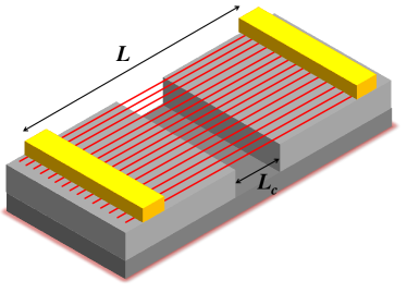
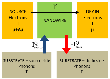
We consider the array of one dimensional (1d) metal-oxide-semiconductor-field-effect-transistors (MOSFETs) shown in Fig. 1. The array is made of many thin doped semiconductor nanowires (NWs) arranged in parallel. Activated transport in each of these NWs corresponds to the multi-terminal setup sketched in Fig. 2. The source and the drain are the two electron reservoirs, whereas the substrate, divided between its source and drain sides, plays the role of a phonon reservoir. The electrons are thermalized in the source and the drain with Fermi-Dirac distribution of temperature and chemical potential . The phonons are thermalized in the substrate with a Bose-Einstein distribution of temperature . If the electron states are localized inside the NWs, but also coupled with the phonons of the substrate, electron transport through the NWs becomes activated when their lengths exceed the Mott hopping length and is governed by Mott’s variable range hopping (VRH) mechanism. Hereafter, we set and where is the electron charge and the bias voltage. We assume a uniform temperature . The bias induces an electron current from the source to the drain. In an activated regime, will be also due to the presence of local heat currents between the nanowire and the substrate. If the nanowire density of states and localization length do not depend on the energy in the vicinity of , fluctuates randomly as a function of the coordinate along the NW, a phonon of the substrate being sometimes absorbed, sometimes emitted. As a consequence, the ensemble average value of the heat exchange vanishes, . Interesting effects occur instead if and are strongly energy dependent. Particle-hole symmetry is broken: This gives rise to large thermoelectric effects [7, 8] and the local heat currents along the NWs become finite, , the phonons being mainly absorbed or emitted near the NW boundaries.
We study such a case using for the density of states per unit length and for the localization length analytical results describing a 1d lattice with random site potentials in the weak disorder limit. Shifting the NW conduction band with the gate voltage such that the electrons are injected from the source around its lower edge, the phonons are mainly absorbed near the source and emitted near the drain. This corresponds to the sketch given in Fig. 2. Inducing with an electric current , one obtains a heat current cooling the source side of the substrate, while heats the drain side. The cooling/heating effects are reversed if the electrons are injected around the upper band edge and vanish if the injection is made around the band center. Phonon absorption/emission can thus be controlled with bias and gate voltages in 1d MOSFETs.
1 VRH transport with energy independent localization length and density of states
Phonon assisted hops between localized states and the associated mechanism of VRH transport have been mainly studied when the energy dependence of the density of the localized states per unit length and of their localization length can be neglected around . Under this assumption, the electron transfer from one localized state to another one separated by a distance and an energy results from the competition between the elastic tunneling probability () to do a hop of length in space and the Boltzmann probability () to do a hop of in energy. This competition gives rise to an optimal hopping length , the Mott’s hopping length, and an optimal hopping energy . In one dimension, one has
| (1) |
| (2) |
Electronic transport is achieved via several hops of magnitude (with ) in space or in energy, and the conductance can be expressed in terms either of or :
| (3) |
Since is a decreasing function of the temperature, the VRH regime takes place above the activation temperature
| (4) |
at which and below the Mott temperature
| (5) |
at which . Below , exceeds the system size and electron transport becomes elastic and coherent (see Ref. [9]). Above , and transport is simply activated between nearest neighbor localized states. Actually, the crossover from VRH to simply activated transport takes place at temperatures lower than in one dimension. This is due to the presence of highly resistive regions in energy-position space, where electrons cannot find available states at distances . These regions behave as ”breaks” that electrons are constraint to cross by thermal activation, resulting in a simply activated temperature dependence of the overall resistance [10, 11].
A more microscopic approach for deriving the above expressions consists in replacing the transport problem by a random-resistor network one [12] in which the hopping between two localized states and is effectively described by a resistor . As proposed by Ambegaokar, Halperin and Langer, one can approximate [13] the resistance of the network by the lowest resistance such that the resistors form a percolating network traversing the sample. In one dimension, an approximation for was derived in Ref. [14]
| (6) |
which predicts a behavior independently of the length when , and a simple activated () behavior for wires longer than .
2 VRH transport in realistic thin nanowires
2.1 Energy dependence of the localization length and density of states
All the previous results were based on the assumption that and are independent of the energy. Such an assumption becomes questionable in one dimension, notably as one approaches the band edges. Let us take the widely used Anderson model: A one dimensional lattice of sites with lattice spacing , nearest neighbor hopping , and random site potentials uniformly distributed in the interval . Its energy levels are distributed in the energy interval , where defines the edges of the NW conduction band when . In the bulk of the band (i.e. for energies ), the density of the Anderson model for small values of and can be described by the formula (valid without disorder)
| (7) |
As one approaches the edges , the disorder effects cannot be neglected and is given by the analytical formula obtained [15] by Derrida and Gardner around :
| (8) |
where and
| (9) |
Similarly, the localization length of the Anderson model can be described by analytical expressions valid for weak disorder. Inside the bulk of the band, one gets
| (10) |
whereas
| (11) |
as approaches the band edges . Figures of the functions and can be found in Ref. [9], where the weak disorder expansions are shown to fit the numerically calculated values of and for values of the disorder parameter as large as .
2.2 Energy dependence of the VRH scales
Using the functions and of the 1d Anderson model and Eq. (1), Eq. (2) and Eq. (6), we show how the Mott hopping length (Fig. 3) and the hopping energy (Fig. 4) vary with . The energy dependence of the resistance which characterizes the best percolation network describing the random resistor network is shown in Fig. 5.
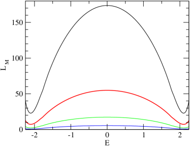
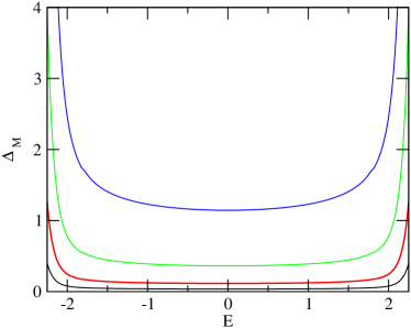
Strictly speaking, these functions , and do not characterize hopping transport in a single Anderson model, but in an ensemble of 1d models where and do not depend on , but rather take uniform values which are given by those of the Anderson model at an energy . Nevertheless, one can easily guess from the figures of , and how an electron will cross the nanowire. If it is injected from the source electrode at an energy around the center of the conduction band, it should exchange much less energy with the substrate (see Fig. 4) and will find much smaller resistances (see Fig. 5) than if it is injected at an energy near the NW band edges. Let us take an electron injected near the lower band edge. It is likely than the percolation path that it will follow will consist first in absorbing many phonons on the NW side close to the source, to reach higher energies where the resistance is weaker (see Fig. 5). Then, it will continue around an optimum energy where it will jump from one localized state to another by emitting or absorbing phonons at random. When it will reach the NW drain side, it will mostly emit phonons, in order to reach an energy of the order of the chemical potential of the drain electrode.
3 Numerical study of the random resistor network
To proceed further, we numerically solve the Miller-Abrahams resistor network [12] which describes hopping transport. The nodes of the network are given by the NW localized states. Each pair of nodes is connected by an effective resistor, which depends on the transition rates induced by local electron-phonon interactions. For a pair of localized states and of energies and , Fermi golden rule [6] gives:
| (12) |
where is the average occupation number of state and is the phonon Bose distribution at energy . The presence of the Heaviside function accounts for the difference between phonon absorption and emission [13]. is the hopping probability due to the absorption/emission of one phonon when is occupied and is empty. Neglecting the energy dependence of and , one obtains in the limit
| (13) |
Here is the distance between the states, whereas , containing the electron-phonon interaction matrix element, depends on the electron-phonon coupling strength and the phonon density of states. Since it is weakly dependent on , and compared to the exponential factors, it is assumed to be constant. From hereon we will take independent of the position along the nanowire 333This is justified if the length of the cut is very small (see Fig. 1): This limit will be assumed to hold in all the numerical simulations that follow.. Under the widely used approximation [13, 16, 17, 18] , Eq. (12) reduces to:
| (14) |
However, we have seen that in one dimension, the energy dependence of and cannot be neglected. Hereafter, instead of using the approximation (14), we will use the exact expression (12) and we will take for
| (15) |
instead of Eq. (13), where
Eq. (15) takes into account the energy dependence of and and
is derived in Ref. [7]. It reduces to Eq. (13) when and
(to leading order) when .
The transition rates between each state and the contacts ( for the source or
for the drain) are assumed do be dominated by elastic tunneling contributions (see Refs. [5, 6]) and read:
| (16) |
where
| (17) |
In the above equations is the contact ’s
Fermi-Dirac distribution, denotes the distance of the state from ,
and is a rate quantifying the coupling between the localized states and the contacts. In the following numerical simulations, we will assume .
Then, the net electric currents flowing between each pair of localized states and
between states and contacts read
| (18a) | ||||
| (18b) | ||||
being the electron charge. Imposing current conservation through all the nodes of the network , one obtains coupled linear equations. Solving numerically this set of equations in the limit where the bias voltage and where the temperature is everywhere gives the unknown occupation numbers of the localized states and hence the linear response solution of the random resistor network problem (see for more details Refs. [6, 7]). This allows us to obtain all the electrical currents and .
The set of energies , of positions and of localization lengths are required as input parameters of the random resistor network problem. Hereafter, we use a simplified model as it is conventional in numerical simulations of VRH transport (see [19, 14, 6]): The are uncorrelated variables taken with a distribution corresponding to the density of the 1d Anderson model [Eqs. (7) and (8)], while the corresponding localization lengths are taken using Eqs. (10) and (11). The positions are taken at random (with a uniform distribution) between and along a chain of length , being the number of sites with spacing .
4 Heat exchange between substrate phonons and NW electrons
4.1 Local heat currents
Let us consider a pair of localized states and , of respective energies and . The heat current absorbed from (or released to) the substrate phonon bath by an electron in the transition reads , being the hopping particle current between and .[7] The local heat current associated to a given localized state is given by summing over all the possible hops with the other NW states :
| (19) |
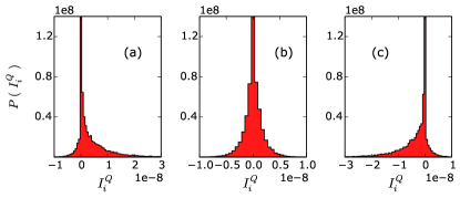
We take the convention that is positive (negative) when it enters (leaves) the NW at site . The probability distribution of is shown in Fig. 6 for states located near three different positions along the NW. The gate potential () has been chosen such that the chemical potential probes the lower band edge of the NW conduction band. Near the source, the distribution is highly asymmetric: The electrons injected in an energy interval of width around the lower band edge need to absorb phonons for reaching higher energies where the paths of the random resistor network are less resistive. Far from the NW boundaries, the distribution becomes symmetric: The electrons have found an optimum value of around which they stay, emitting or absorbing phonons at random. Near the drain, the distribution becomes again asymmetric, as the electrons emit more phonons to decrease their energies to reach the chemical potential of the drain.
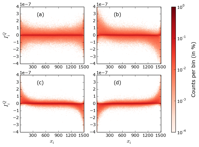
In Fig. 7 we show 2d histograms of the local heat currents as a function of the position inside the NW. The data have been calculated for a temperature and four different values of , corresponding to electron injection at the band center (), below the band center () and around the lower () and upper () band edges of the NW conduction band, respectively. At the band center, the fluctuations of the local heat currents are symmetric around a zero average. They are larger near the NW boundaries and remain independent of the coordinate otherwise. Away from the band center, one can see that the fluctuations are not symmetric near the NW boundaries, though they become symmetric again far from the boundaries. When the electrons are injected through the NW in the lower energy part of the NW band, more phonons of the substrate are absorbed than emitted near the source electrode. The effect is reversed when the electrons are injected in the higher energy part of the band (by taking a negative gate potential ): It is now near the drain that the phonons are mainly absorbed. The 2d histograms corresponding to and are symmetric by inversion with respect to .
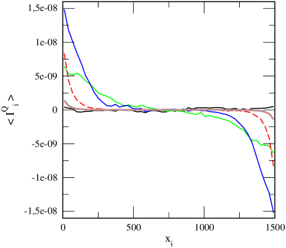
In Fig. 8, one can see how varies the mean value of the local heat current along the nanowire for different values of . Though the heat current extracted from the substrate near the source takes larger local values when one probes the band edges, one can see that it is more advantageous for cooling the source side of the substrate to inject the electrons at an intermediate energy, when (see also Sec. 4.3).
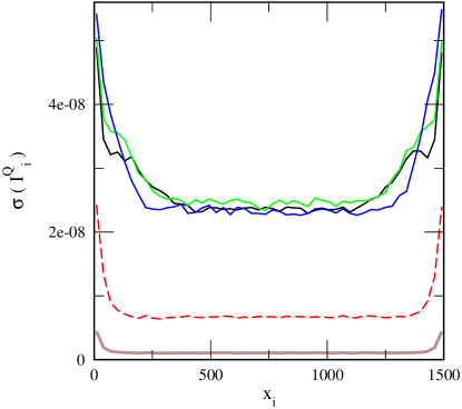
In Fig. 9, one can see how the standard deviation of the local heat currents varies as a function of the position along the nanowire, using the same parameters and color code than in Fig. 8. The fluctuations of the local heat currents are strongly reduced when the electrons are injected near the band edges, and become independent of the injection energy if this energy is taken around the band center.
4.2 Total heat current extracted from the source side of the substrate
As sketched in Fig. 1, we assume that the substrate has a small cut over which the NW is suspended, and we are interested in cooling the substrate on one side of the cut, while the other side would be heated. Assuming that the contribution of the NW center can be neglected (or that the cut is very short), the total heat current extracted from the source side of the substrate using a NW of length is defined as
| (20) |
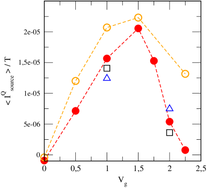
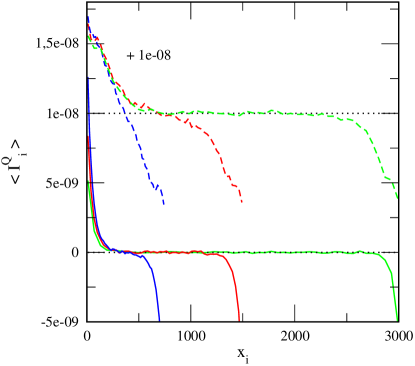
i.e. gives the area under the curves shown in Fig. 8, taken from to . is shown as a function of for and in Fig. 10. One can see that the cooling effect is maximum when . Very approximately, in the studied temperature domain and does not depend on . The existence of an asymptotic regime when is confirmed in Fig. 11. The average local heat currents do not depend on near the NW boundaries and vanish in its middle.
4.3 Optimum condition for phonon absorption by the first half of a NW
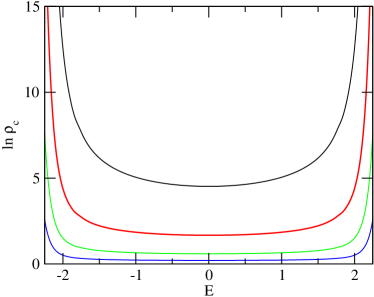
In Fig. 10, one can see that gives the largest value for . This optimal value comes from the competition between two effects. On the one side, injecting electrons of energies near the lower band edge favors phonon absorption. On the other side, at these energies the resistance of the random resistor network is very large (see Fig. 5), at least near the NW boundaries. This necessarily reduces the particle current crossing the NW, and hence the heat current extracted from the source side of the substrate. For a few disordered chains, we have studied the map of currents larger than some threshold value which are driven by the bias voltage. Around the lower band edge (), it does not seem that the electrons are able to hop high enough in energy for reaching the band center where is minimum. Despite very large sample to sample fluctuations, the currents connecting states of positions and located around the middle of the NW have energies and mainly located at a distance below the band center. could correspond to the largest energy distance over which the electrons can hop for reaching the band center in the middle of the NW. The difficulty of reaching energies far from the chemical potential can be understood by looking at the expression (14) for the transition rates.
4.4 Order of magnitude of heat fluxes using arrays of parallel NWs
In Fig. 10, the total heat current integrated over the first half of a single NW is given in units of . We take the parameters values used in Ref. [8]: K gives meV. This implies for a maximum value around pW when , K and . The used bias corresponds to a very small voltage V. Assuming that the non linear effects remain negligible by increasing the bias to a larger value, say mV corresponding to , one would have a maximum value nW for a single NW of a length m. This length corresponds to a lattice of 700 sites with a spacing of nm.
Larger cooling power could be obtained by taking very large arrays of parallel NWs, as sketched in Fig. 1 for 15 NWs only. Let us take a packing density for a 2d NWs array. This corresponds to a NW diameter nm and a NW interspacing of nm. parallel NWs would make an array of width cm. It could be used for extracting mW from the source side of the substrate, in a cm large and a few m long area located near the source electrode. This estimated value of mW is done assuming at a temperature K and a bias mV. It could be increased by increasing or , if VRH transport holds at larger temperatures and if the linear response theory remains valid at larger bias voltages. Additional results concerning the perspectives given by large arrays of 1d MOSFETs for energy harvesting and hot spot cooling can be found in Ref. [8]).
5 Summary
We have considered phonon assisted transport between localized states using a model characterized by the density of states and the localization length of the 1d Anderson model, going beyond theories where the energy dependence of and are neglected. We have studied the distributions of the heat currents characterizing locally the heat exchange between the substrate phonons and the NW electrons, as one shifts with a gate the NW conduction band. From those local heat currents, the structure of the percolative network connecting states of different energies and locations can be guessed. When the electrons are injected in the middle of the conduction band, the percolative path consists mainly of states with energy in an energy interval of width around the band center. Even in this case, Fig. 7 (a) shows us that the heat currents have larger fluctuations near the NW boundaries that in its bulk. This has to be related to the observation made in Ref. [6] that the thermopower in the hopping regime is governed by the edges of the samples. When electrons are injected around the band edges, the boundary effects upon the local heat currents become much larger. It becomes possible to have mainly phonon absorption at one NW boundary, and phonon emission at the other, instead of spreading phonon emission and absorption along the NW. In Refs. [7, 8], the thermoelectric effects of gated disordered NWs have been studied in the hopping regime. In this work, we have focused the study on the heat exchanges occurring between the NW electrons and the substrate phonons. The obtained results lead us to put forward arrays of 1d MOSFETs as tools for managing heat at submicron scales. Moreover, such tools make possible to control phonon absorption/emission by varying the gate and bias voltages.
References
- [1] M. Buttiker, Four-terminal phase-coherent conductance, Phys. Rev. Lett. 57 (1986) 1761.
- [2] R. Sanchez, M. Markus Buttiker, Optimal energy quanta to current conversion, Phys. Rev. B 83 (2011) 085428.
- [3] B. Roche, P. Roulleau, T. Jullien, Y. Jompol, I. Farrer, D. A. Ritchie, G. D. C., Harvesting dissipated energy with a mesoscopic ratchet, Nature Communications 6 (2015) 6738.
- [4] F. Hartmann, P. Pfeffer, S. Hofling, M. Kamp, W. L., Voltage fluctuation to current converter with coulomb-coupled quantum dots, Phys. Rev. Lett. 114 (2015) 146805.
- [5] J.-H. Jiang, O. Entin-Wohlman, Y. Imry, Thermoelectric three-terminal hopping transport through one-dimensional nanosystems, Phys. Rev. B 85 (2012) 075412.
- [6] J.-H. Jiang, O. Entin-Wohlman, Y. Imry, Hopping thermoelectric transport in finite systems: Boundary effects, Phys. Rev. B 87 (2013) 205420.
- [7] R. Bosisio, C. Gorini, G. Fleury, J.-L. Pichard, Gate-modulated thermoelectric conversion of 1-d disordered nanowires: Variable-range hopping regime, New J. Phys. 16 (2014) 095005.
- [8] R. Bosisio, C. Gorini, G. Fleury, J.-L. Pichard, Using activated transport in parallel nanowires for energy harvesting and hot-spot cooling, Phys. Rev. Applied 3 (2015) 054002.
- [9] R. Bosisio, G. Fleury, J.-L. Pichard, Gate-modulated thermopower in disordered nanowires: I. low temperature coherent regime, New J. Phys. 16 (2014) 035004.
- [10] J. Kurkijärvi, Hopping conductivity in one dimension, Phys. Rev. B 8 (1973) 922.
- [11] M. E. Raikh, I. M. Ruzin, Sov. Phys. JETP 68 (1989) 642.
- [12] A. Miller, E. Abrahams, Impurity conduction at low concentrations, Phys. Rev. 120 (1960) 745.
- [13] V. Ambegaokar, B. I. Halperin, J. S. Langer, Hopping conductivity in disordered systems, Phys. Rev. B 4 (1971) 2612.
- [14] R. A. Serota, R. K. Kalia, P. A. Lee, New aspects of variable-range hopping in finite one-dimensional wires, Phys. Rev. B 33 (1986) 8441.
- [15] B. Derrida, E. Gardner, Lyapounov exponent of the one dimensional anderson model: weak disorder expansions, J. Physique 45 (1984) 1283.
- [16] M. Pollack, Hopping transport in solids, J. Non-Cryst. Solids 11 (1972) 1.
- [17] B. Shklovskii, A. Efros, Electronic Properties of Doped Semiconductors, Springer-Verlag, Berlin, 1984.
- [18] I. P. Zvyagin, On the theory of hopping transport in disordered semiconductors, Phys. Stat. Sol. (b) 58 (1973) 443.
- [19] P. A. Lee, Variable-range hopping in finite one-dimensional wires, Phys. Rev. Lett. 53 (1984) 2042.