Spatial dispersion effects upon local excitation of extrinsic plasmons in a graphene micro-disk
Abstract
Excitation of surface plasmon waves in extrinsic graphene is studied using a full-wave electromagnetic field solver as analysis engine. Particular emphasis is placed on the role played by spatial dispersion due to the finite size of the two-dimensional material at the micro-scale. A simple instructive set up is considered where the near field of a wire antenna is held at sub-micrometric distance from a disk-shaped graphene patch. The key-input of the simulation is the graphene conductivity tensor at terahertz frequencies, being modeled by the Boltzmann transport equation for the valence and conduction electrons at the Dirac points (where a linear wave-vector dependence of the band energies is assumed). The conductivity equation is worked out in different levels of approximations, based on the relaxation time ansatz with an additional constraint for particle number conservation. Both drift and diffusion currents are shown to significantly contribute to the spatially dispersive anisotropic features of micro-scale graphene. More generally, spatial dispersion effects are predicted to influence not only plasmon propagation free of external sources, but also typical scanning probe microscopy configurations. The paper set the focus on plasmon excitation phenomena induced by near field probes, being a central issue for the design of optical devices and photonic circuits.
I Introduction
One of the main challenges for current device electronics is the full exploitation of the terahertz (THz) electromagnetic (EM) spectrum, bridging the gap beitween the microwaves and optics. In this context, graphene and graphene-derived materials possess a number of unique EM properties such as tunable conductivity and slow-wave features that may be used to develop high performance THz devices 1 ; 2 ; 3 ; 4 ; 5 ; 5b ; 6 . More generally, low-dimensional systems with honeycomb-like geometry and related assemblies or hetero-structure are undergoing massive investigation as materials capable of supporting plasmon propagation in the THz frequency range 7 ; 7b ; 7c ; 7d ; 8b .
A THz beam impinging on a metal atomic force microscope tip has been used to generate guided THz waves on graphene in a recent experiment 7 : the nanometric curvature of the tip makes light scatter on the length scale of tens of nanometers 2 , providing the EM field together with the wave-number components required to excite short wavelength surface plasmons. A similar situation has been encountered at lower frequencies in scanning microwave microscopy (SMM) 8 , where a metallic tip can act as a resonant antenna whose tip-termination is directly coupled with the sample.
In this paper, we focus on numerical propagation and excitation of plasmon surface waves in spatially dispersive graphene as seen from the macroscopic EM perspective. We use the fact that a momentum matching between the field source and the surface plasmon can be achieved, e.g., by grating or prism couplers. In particular, we present an EM scheme that ideally recalls the set-up of Ref. 8 and take a resonant wire antenna placed at sub-micrometric distance from a disk-shaped graphene patch.
Our analysis suggests that the correction to the conductivity response given by spatial dispersion is strongly required, at least in excitation phenomena induced by a strong spatial gradient of the EM field on the sample. We therefore asses that spatial dispersion is an important limiting factor to the achievable coupling between surface-plasmons and the near field of an SMM tip, because it produces a broadening of the system-response over a wide range of wave-vectors. The high impact of spatial dispersion in propagation and modal analysis of plasmons has been previously scrutinized 9 ; 10 ; 11 . However, a similar study has not been conducted so far in near field excitation problems, which are of central importance in numerous practical applications including microscopy and photonics. Here, we provide such a characterization.
From the numerical point of view, we simulate surface plasmon excitation in an open computational domain avoiding periodic boundary conditions and plane-wave excitations 5 . The typical high charge mobility of carbon nanostructures leads to a huge increase of the macroscopic inductance, i.e., a high reactive energy stored per unit length and, accordingly, a slow-wave propagation. Consequently, the plasmon velocity can be much smaller than the speed of light with very small wavelengths as compared to that of the coupled feeding antenna. This also results in a high confinement of the EM field in the direction transverse to the propagation, which further increases the aspect ratio. We then apply two different numerical methods to validate the results, i.e., the method of moments (MoM) and the method of finite elements (FEM). In this way, we provide a comparison of the different levels of approximation used in semi-classical approaches to the graphene conductivity, based on the Boltzmann transport equation for the Dirac electrons and the Kubo-formula 12b ; 12c ; 12cc ; 12 ; 12o .
II Theory
The dispersive conductivity of graphene on the THz regime is well defined in the literature 1 ; 10 ; 11 : basically, an electric field frequency below a few THz induces a response of the valence () and conduction () electrons of the material with an energy close to the Fermi energy. The dominant part of the response in extrinsic (doped or gated) graphene is given by intra-band excitations, which can be treated by the Boltzmann transport equation under the relaxation-time-approximation (RTA) or Bhatnagar-Gross-Krook (BGK) model.
The RTA replaces the relaxation dynamics of each one-electron state by a simple exponential decay. Then, the transport relaxation time is approximated with the lifetime of the state. Such a formalism provides an accurate description of spatial dispersion effects in doped graphene with extrinsic Fermi energy shifts below eV. Accordingly, the RTA conductivity is entirely determined by the drift currents that arise from one-electron transitions and collective modes within the and bands.
The BGK model is more general than the RTA, because it allows for an extra degree of freedom, which enforces charge conservation and accounts properly for electron diffusion 10 ; 11 .
We begin by specializing to the RTA conductivity
under an applied electric field with momentum and frequency . includes the contributions of electrons (with charge and wave-vector ) that occupy the (+) and (-) bands. The band energies are populated according to the Fermi Distribution (FD)
at the absolute temperature and chemical potential . We adopt the widely used convention of setting the Dirac point energy of graphene, i.e. the intrinsic Fermi level, to zero energy. In this way, coincides with the Fermi level shift caused by the doping (or gating).
The intra-band components of have the dyadic (tensor) form 10
| (1) |
where: (i) the band energies are linearized as , with representing the electron velocities and the Fermi velocity; (ii) is the first energy-derivative of the FD, i.e.,
(iii) is a complex frequency that includes the angular frequency and a small shift along the imaginary axes, which corresponds to the electron damping rate ; the latter depends on the average relaxation time as .
In Eq. (1), the (two-dimensional) first Brilluoin Zone (BZ) integration is well defined on circular areas of the -space centered at the Dirac points, where the linear approximation for the band energies is valid. Nevertheless, in most practical uses, an infinite cone-structure is assumed for the valence and conduction bands; in other words, the wave-vector integral is performed over the whole -space for analytical convenience and a factor of is included to account for the inequivalent Dirac point. Then, a change of variable from wave-vector to the energy leads to the non-dispersive conductivities , in which
and denotes the identity matrix. The total intra-band conductivity at is then
Interestingly enough, the RTA conductivity (1) and its form (II) can be derived from the Kubo formula in the optical limit 12b ; 12c ; 12cc ; 12 ; 12o .
Another part of the graphene conductivity is related to inter-band processes between the and bands, and is also included in the Kubo formulism 12c ; 12cc ; 12 ; 12o , though it does not contain the dispersive term . Indeed, it has been pointed out that for surface waves supported by isolated graphene sheets, and working frequencies below a few THz, the spatial dispersion effects on inter-band transitions can be neglected 10 ; 11 . Due to the absence of the dispersive term, the inter-band conductivity is a scalar, which can be expressed as
| (3) |
Therefore, the total conductivity reads
| (4) |
In the -limit the latter tends to the non-dispersive Kubo conductivity 12c ; 12cc ; 12 ; 12o :
| (5) |
Now, looking at the denominator in Eq. (1), it is clear that when and are comparable, spatial dispersion cannot be neglected in surface plasmon excitation. This happens particularly in problems where a resonant behavior of the EM field is concerned. It is the case of some of the examples reported in this work, where the interaction between a radiating antenna and a graphene patch takes place via near field coupling.
To give an idea of the numbers involved, the spatial harmonics of the excitation field become significant in the conductivity response at an operating frequency of the order of THz, for an applied wave-vector value larger than m-1. At the same frequency, the electric field wavelength is about m. However, the near field distribution between the tip of the antenna and the graphene sample varies on a sub-micrometric scale, depending on the tip radius and distance from the sample. Then, the slow-wave effect featured by plasmon propagation implies a wavelength reduction of more than one order of magnitude, and ensures the matching and coupling with the exciting near field.
Eq. (1) can be simplified and made more explicit by expressing the planar wave-vectors and in polar coordinates, say, and . Then, as shown in the appendix, we can reduce it to the following expression
| (9) | |||||
where the BZ integral has been turned to a wave-vector integral over the whole -space (with the factor of from the inequivalent Dirac points being included).
After some straightforward manipulations on the angular integral in Eq. (9) that are reported in the appendix, we obtain the tensor components of the intra-band conductivity
| (10) |
which depend on the scalar conductivities
and
These two quantites may rewritten as
and
Therefore, summing over the channels, we find
and
Then, and turn out to be both proportional to the non-dispersive intra-band conductivity of Eq. (II), which evaluates exactly to with
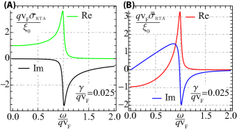
Incidentally, we notice that the conductivity , being markedly anisotropic, is proportional to . This makes its imaginary part change sign with increasing the frequency, in contrast to the purely inductive nature of , whose imaginary part keeps a negative sign in the sampled frequency range. The plots of Fig. 1(A) and 1(B) illustrate such a behavior. Now, by definition, surface waves are sustained at the interface between materials having different permittivities so that, in a transverse resonance circuit, their associated reactances cancel out. Therefore, the contribution of the anisotropic term may strongly affect the polarization of surface plasmons 14 of high rate of spatial variation.
To include the diffusion currents, we introduce the following tensor quantity
| (11) |
where
The BGK correction to the RTA conductivity can be put in the form
| (12) |
This is equivalent to the result presented in Ref. 10 , and leads to correct the total conductivity as
| (13) |
The numerical results reported in the following are obtained by both a full-wave solver and a semi-analytical approach, as implemented respectively by the finite element method (FEM) and the method of moments (MoM). The latter employs the usual free-space Green’s tensor , in cylindrical coordinates and , as the kernel of an integral operator relating the electric current density and field 12 ; 12o :
Here, it should be noticed that the discretized currents in space are assumed as independent variables in the MoM calculation. Then, the solution for the resulting Electric Field Integral Equation (EFIE) is generalized to the case of spatially dispersive material 11 ; 12 ; 12o , by using the proper constitutive relation in the spatial domain, i.e.,
| (14) |
In this equation, the planar current , and the tangent electric field , are sampled over the graphene surface.
The non-local behavior of the current-field relation becomes important when rapid field variations are involved. Transforming the conductivity in real space, the input spatial response of dispersive graphene is obtained as
| (18) | |||||
where the scalar conductivities and include both the -contributions from Eq. (10) or Eq. (12). In Eq. (18) the first and second terms contributing to the conductance, are weighted by the zero-order and second-order Bessel functions, respectively. This means that the first addend of the conductivity is more sensitive to slow varying fields with respect to the second addend. Equally importantly, the second term of the conductivity, containing off-diagonal matrix elements, is characterized by an angular dependence related to a current response, which is locally weighted by a “quadrupole” spatial distribution of the EM field. Consequently, unless very high angular and radial variations of the EM fields are concerned, the second term can be neglected.
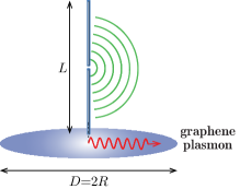
Let us now turn to the main application of the present work (Fig. 2) that is a circular graphene disk of diameter , with a wire antenna of length , placed just above its center. For this system, we can safely assume cylindrical symmetry. The gap between the antenna and the disk is . In absence of angular variation of the EM excitation, the off diagonal terms vanish and no angular current arises. In addition, with a not too small tip-sample distance, and, thus, a not too strong EM field variation, the -term in Eq. (18) is expected to be dominant. Under these limiting conditions, Eq. (14) can be approximated by
| (19) |
where is the radial component of the surface current, and is the real space representation of , which gives the (spatial) impulsive response of the current after the EM excitation. Note that usual assumption of a thin hollow cylinder to approximate the wire antenna may affect the near field distribution between the tip and graphene, but it does not limit the generality of the present analysis.
For a fixed frequency, the effect of spatial dispersion increases with increasing the charge scattering-time. As a practical example, we take the cumulative integral of the impulsive response
i.e., the current density response to a uniform unit electric field within a circular area of radius . Its profile, normalized to , is shown in Fig. 3 for two different scattering times ( ps), at THz.
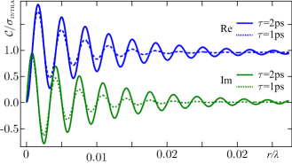
In absence of dispersion, the response of Fig. 3 would be a real constant without spatial ripples. In presence of dispersion, the actual response is more complex, and some spatial ripples appear. These oscillations extend just to a fraction of the free-space wavelength , which is typically comparable with the plasmon wavelength, and increases with increasing the charge lifetime. We expect that the above behavior of the system will reflect, numerically, on the solution of the EM field distribution.
III Numerical Results
In the following, we present the solution for the EFIE directly in real space, focussing on both the full tensor form (18) and the scalar form (19) of the surface conductivity.
III.1 Non-Dispersive Analysis of Surface Plasmons
We begin by considering an example of plasmon excitation without spatial dispersion. Let us define the graphene surface impedance as the reciprocal of the non-dispersive Kubo conductivity introduced in Sec. II. We then have or , where the intra-band and inter-band terms have been respectively given in Eqs. (II) and (3).
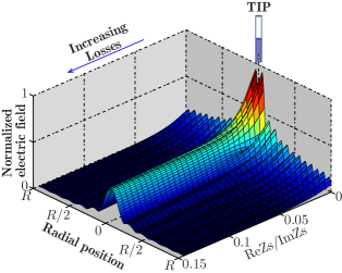
The plasmon distribution for a graphene disk of diameter , coupled to an antenna of length , is reported in Fig. 4 vs the radial position within the disk and the inverse plasmon “quality factor”. The latter is defined as the ratio between imaginary and real parts of calculated by the non-dispersive Kubo conductivity, i.e., . In Fig. 4, both the operation frequency and the graphene chemical potential follow from the choice of the surface reactance and plasmon quality-factor. For example, a reactance of k and a quality factor of are associated to a chemical potential of eV and a frequency of about THz. We see that the spatial oscillations and propagation of the plasmon expire, at a progressively smaller radial distance from the feeding tip, as increases from to .
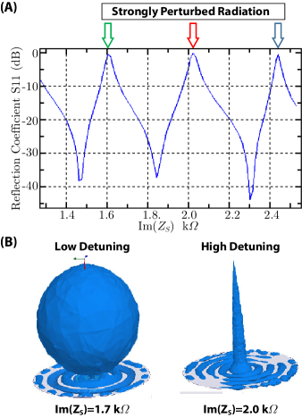
Another interesting effect is pointed out in Fig. 5, where the overlap of the plasmon distribution with the near field under the tip determines the strength of the coupling and the amount of power transferred from the antenna to the plasmon. In order to emphasize this concept- and make the effect more evident- the losses are just neglected. More specifically, the surface resistivity is taken to be an independent variable, i.e., its value is not calculated from the Kubo conductivity as in Fig. 4. In addition, is considered a purely imaginary quantity (no losses) and the reactance is varied from about k to k. Thus, the geometric parameters may be expressed in terms of the sizes of the antenna and the graphene disk relative to the vacuum wavelength . In particular: (i) the diameter of the patch and the length of the wire antenna are related by ; (ii) the air-gap distance between the antenna and the graphene-patch is given by ; (iii) the radius of the antenna is fixed to ; (iv) a value of is chosen for the excitation-gap in the middle of the antenna, where the voltage-source is applied; (v) The internal impedance of the voltage applied to the excitation-gap of the antenna is set to .
It should be noted that the value of can be scaled up or down provided that it remains much smaller than and that the applied voltage is scaled reversely. In addition, the internal impedance value is equal to the real part of the input impedance of the antenna in absence of graphene to have maximum power transfer. Fig. 5(A) shows that the antenna, which would work precisely at its resonance frequency in absence of graphene, can be more or less “detuned” by the graphene patch. The detuning depends on the graphene-antenna coupling: the higher the coupling strength, the higher the coupled reactive power, and the higher the reflection coefficient at the input port of the antenna (indicated by arrows). expresses the amount of power that is reflected back at the terminals of a voltage-source excitation, given by an infinitesimal electric dipole located at the center of the antenna. By definition, we have . The choice of the source impedance of the voltage excitation is arbitrary. However, as stated above, we have set in order to have resonance in absence of graphene, and accordingly a better visualization of the perturbing effect of the graphene patch (see Sec. III.2 for more information and numerical values). Fig. 5(B) shows in details what is happening to the antenna near (right picture) and far from (left picture) the detuning points, i.e., the arrows of Fig. 5(A). In particular, we have taken surface reactance values of and k, corresponding respectively to input matching values of about and dB: in the former case, the radiation is drastically reduced by the plasmon coupling and a large amount of power is reflected back to the input port of the antenna. The results reported in Fig. 5(A) are derived from our MoM simulator 15 , whereas the plots of Fig. 5(B) are calculated by a full-wave EM solver (HFSS by Ansoft), which provides an independent validation of our implementation.
III.2 Dispersive Characterization of Surface Plasmons
In order to discuss the effect of dispersion on the strength of plasmon excitation, we focus on the two examples reported in Fig. 6. Differently from the results shown in Fig. 5, here we take into account ohmic losses using the approximate complex conductivity of Eq. (19) within the RTA limit. Assuming a nominal frequency of THz, we show the effect of spatial dispersion on the input matching (S11) of the antenna in resonant [, Fig. 6(A)] and non-resonant [, Fig. 6(B)] conditions, respectively. All the reflection coefficients at the input terminal of the antenna are plotted as function of the chemical potential of graphene, i.e., the Fermi energy shift associated to the local doping level.
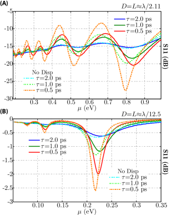
Three typical values of charge-carrier relaxation times on the ps time-scale are tested ( ps). Indeed, the relaxation time in graphene may strongly depend on the quality of the sample related to the fabrication process. In particular, real samples are affected by the presence of grain boundaries, defects, multilayer regions, etc. For the above reason, some flexibility is needed in selecting the parameter. As evident from Fig. 6, the larger is the relaxation time the sharper are the S11 peaks that express the maxima and minima of the antenna-plasmon coupling. The antenna is fed by a voltage source with an impedance equal to the real part of the input impedance of the antenna, which is about and for the resonant and non-resonant cases, respectively. Clearly, the minima of reflection, corresponding to surface field resonances, have lower matching levels in the non-resonant case. In either resonant or non resonant condition, the dispersive reflection peaks are more broadened- and have lower maxima- with respect to the corresponding non-dispersive ones. These differences become more and more evident as the relaxation time increases, or, the quality of graphene gets better.
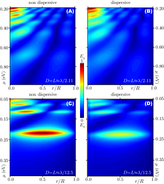
In SMM, an electrostatic tuning of the charge density with a DC voltage applied to the microscope tip 7 can provide the local doping for near field applications. Fig. 7 shows the spatial distributions of the plasmonic wave on the graphene disk (for a normalized electric field) as function of the radial position and the doping levels (values corresponding to those of Fig. 6). The distributions are computed with and without spatial dispersion, assuming a relaxation time of ps. Differences between the dispersing and non dispersing curves are clearly observable, particularly in correspondence of the resonance peaks. Looking at the plots of Fig. 6 and Fig. 7, we see that the absolute effect of spatial dispersion is higher in the non-resonant case, where the size of the graphene disk is much smaller than the free-space wavelength .
To go beyond the diagonal conductivity approximation of Eq. (19) in the RTA, we explicitly account for the angular variations of the EM field and, at the same time, we include the effect of diffusion currents. Thus, we next consider the full conductivity response of Eq. (18), within both the RTA and BGK approach. In Fig 8, we report the details of the input matching of the antenna in the resonant case , comparing the results obtained from the different levels of approximations discussed in the present work. We find confirmation that the RTA conductivity of the graphene disk represents a significant improvement with respect to the non-dispersive conductivity of an infinite graphene sheet. In addition, we see that the contribution of the off diagonal tensor leads to a non-negligible small correction to the diagonal tensor , within the RTA.
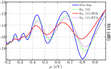
More importantly, we notice that the effect of electron diffusion included in the BGK model plays a significant role. Indeed the RTA and BGK expressions of and are remarkably different: dispersion effects appear to be under-estimated by the RTA conductivity [or even more simplified expressions as Eq. (19)] with respect to the BGK form.
IV Conclusions
We have used a semiclassical model derived from the Boltzmann transport equation to investigate the effect of spatial dispersion on the linear THz response of graphene, characterized by excitation of surface plasmons. The excitation source has been provided by the near field of an antenna radiating in proximity of a graphene micro-disk.
We have characterized the role of spatial dispersion, with respect to a cylindrical system, within both the RTA and the BGK approach, obtaining meaningful and compact expressions of the full-tensor representing the constitutive relation of the graphene patch in real space.
We have shown that the surface distribution of the field on the disk, and the macroscopic response of the antenna, is significantly affected by spatial dispersion in two distinct noteworthy examples, where the antenna has been set in resonant and non-resonant conditions.
Although the role played by spatial dispersion was previously clarified in propagation and modal analysis of plasmons 10 ; 11 , here we have provided a focus on near field excitation problems, with potential fallout in important practical applications, concerning near field imaging.
Acknowledgements.
This work has been supported by the European Project “Carbon Based Smart Systems for Wireless Applications”, (NANO-RF, n. 318352). We also thank NOW Srli (www.notonlywaves.com) for providing HFSS simulations.References
- (1) F. H. L. Koppens, D. E. Chang, and F. J. G. de Abajo, Nano Letters 11, 3370 (2011).
- (2) L. Ju et al., Nature nanotechnology 6, 630 (2011).
- (3) T. Echtermeyer et al., Nature communications 2, 458 (2011).
- (4) J. Christensen, A. Manjavacas, S. Thongrattanasiri, F. H. Koppens, and F. J. García de Abajo, ACS nano 6, 431 (2011).
- (5) D. A. Smirnova, R. E. Noskov, L. A. Smirnov, and Y. S. Kivshar, Physical Review B 91, 075409 (2015).
- (6) B. Diaconescu et al., Nature 448, 57 (2007).
- (7) R. R. Hartmann, J. Kono, and M. Portnoi, Nanotechnology 25, 322001 (2014).
- (8) T. Low and P. Avouris, Acs Nano 8, 1086 (2014).
- (9) A. N. Grigorenko, M. Polini, and K. Novoselov, Nature photonics 6, 749 (2012).
- (10) K. S. Novoselov et al., Nature 490, 192 (2012).
- (11) F. J. Garcia de Abajo, Acs Photonics 1, 135 (2014).
- (12) M. Pisarra, A. Sindona, P. Riccardi, V. Silkin, and J. Pitarke, New Journal of Physics 16, 083003 (2014).
- (13) M. Farina et al., Nature communications 4 (2013).
- (14) D. Correas-Serrano, J. S. Gomez-Diaz, and A. Alvarez-Melcon, Antennas and Wireless Propagation Letters, IEEE 13, 345 (2014).
- (15) G. Lovat, G. W. Hanson, R. Araneo, and P. Burghignoli, Physical Review B 87, 115429 (2013).
- (16) D. Correas-Serrano, J. S. Gomez-Diaz, J. Perruisseau-Carrier, and A. Alvarez-Melcon, Microwave Theory and Techniques, IEEE Transactions on 61, 4333 (2013).
- (17) Chapter 6 electron transport, in Conceptual Foundations of Materials: A Standard Model for Ground- and Excited-State Properties, edited by S. G. Louie and M. L. Cohen, , Contemporary Concepts of Condensed Matter Science Vol. 2, pp. 165 – 218, Elsevier, 2006.
- (18) V. Gusynin, S. Sharapov, and J. Carbotte, Journal of Physics: Condensed Matter 19, 026222 (2007).
- (19) V. Gusynin, S. Sharapov, and J. Carbotte, Physical Review B 75, 165407 (2007).
- (20) G. W. Hanson, Journal of Applied Physics 103, 064302 (2008).
- (21) G. W. Hanson, Antennas and Propagation, IEEE Transactions on 56, 747 (2008).
- (22) D. Mencarelli, L. Pierantoni, A. di Donato, and M. Farina, Journal of Computational Electronics 14, 214 (2015).
- (23) X. Y. He and R. Li, IEEE Journal of selected topics in quantum electronics 20, 62 (2014).
- (24) I. Gradshteyn and I. Ryzhik, Table of integrals, series, and products, 7 Ed. (Academic Press NY, 2007).
Appendix: Dispersive and Non-Dispersive RTA conductivity
Using the polar coordinates and , the tensor product at the numerator of the BZ integral in Eq. (1) becomes
while the scalar products at the denominator reads: . Hence, Eq. 1 is turned to Eq. 9. Now, consider the integral identity
which holds true for and , and can be derived from the database 13 . As special cases, we get
for and
for . By a simple change of variable, we also have:
It follows that the -integral in Eq. (9) evaluates to
Plugging this in to Eq. (9), we obtain Eq. (10) and the scalar conductivities , .