Modulating spin relaxation in nanowires with infrared light at room temperature
Abstract
Spintronic devices usually rely on long spin relaxation times
and/or lengths for
optimum performance. Therefore, the ability to modulate these quantities with an
external agent offers unique possibilities. The dominant
spin relaxation mechanism in most technologically important semiconductors
is the D’yakonov-Perel’ (DP) mechanism which vanishes if the spin carriers
(electrons) are confined to a single conduction subband in a quantum wire
grown in certain crystallographic directions, or polycrystalline quantum wires. Here, we report modulating
the DP spin relaxation rate (and hence the spin relaxation length)
in self assembled 50-nm diameter
InSb nanowires with infrared light at room temperature.
In the dark, almost all the electrons in
the nanowires are in the lowest conduction subband at room temperature, resulting in
near-complete absence of DP relaxation. This allows observation of spin-sensitive effects in the
magnetoresistance. Under infrared illumination, electrons are photoexcited to
higher subbands
and the DP spin relaxation
mechanism is revived, leading to a three-fold decrease in the spin relaxation length. Consequently, the
spin sensitive effects are no longer observable under illumination. This phenomenon may have applications
in spintronic
room-temperature infrared photodetection.
KEYWORDS D’yakonov-Perel’ spin relaxation, nanowires, subband effects, spintronic infrared photodetection.
Introduction
It is well-known that the D’yakonov-Perel’ (DP) spin relaxation mechanism [1] is completely absent in a semiconductor quantum wire of certain crystallographic orientations if only the lowest conduction subband state is occupied by electrons (spin carriers) [2, 3]. In narrow gap semiconductors (e.g. InSb, InAs), or in polycrystalline samples, where the Rashba interaction [4] would be far stronger than the Dresselhaus interaction [5], single subband occupancy will nearly eliminate any DP relaxation regardless of the wire’s crystallographic orientation. Since the DP relaxation is the dominant spin relaxation mechanism in compound semiconductors like InSb [6, 7, 8, 9, 10, 11] at room temperature, its elimination can increase the spin relaxation time and spin relaxation length in these semiconductors considerably. That is an important result since spin-relaxation is the spoiler in most spin-based devices and applications.
There have been theoretical predictions that the DP spin relaxation rate will decrease in quantum wires compared to bulk or quantum well systems [12, 13, 14, 15] and this has been borne out by experiments [16, 17]. Ref. [16] studied InSb nanowires where 96% of the electrons were expected to reside in the lowest conduction subband and found that at room temperature the total spin relaxation time had increased by an order of magnitude over that reported in bulk or quantum wells, despite poorer electron mobility in the nanowires. This result was attributed to strong suppression of the DP relaxation. However, these experiments are not confirmatory proofs that the elimination/suppression was purely due to single/few subband occupancy since confirmation would require showing that the spin relaxation time is controllably increased by controllably exciting electrons from the lower to the higher subbands.
In this paper, we report controlled modulation of the DP relaxation rate at room temperature in 50-nm diameter InSb nanowires by varying the subband population with an external agent. This leads to controlled modulation of the net spin diffusion length. The obvious approach to vary subband population controllably would have been to use split-gate quantum point contacts that allow varying the nanowire width (and hence the subband population) with a gate potential [18, 19]. In comparison, our approach to use infrared (IR) light to excite electrons continuously to higher subbands from the lowest one – thereby causing multi-subband transport – is much easier since it does not require making a gate contact. Furthermore, varying the nanowire width with a split gate, or simply using different nanowires with different diameters [17], does not provide an unambiguous picture of how the DP relaxation rate depends on subband occupation because changing diameter could affect the carrier mobility (which is mostly governed by interface roughness scattering) and thus affect other spin relaxation rates, notably the Elliott-Yafet [20]. This problem is somewhat mitigated if the subband occupation is changed with light. The k-selection rule guarantees that the electron’s momentum before and after photon absorption are approximately equal, so light does not affect the Elliott-Yafet spin relaxation directly because that requires a change in electron momentum. However, occupation of higher subbands can change carrier mobility by promoting inter-subband scattering and this can affect the Elliott-Yafet rate. Fortunately, this effect is weak because the mobility in the nanowires we fabricate is governed primarily by interface roughness scattering and not inter-subband scattering. Therefore, any light-induced change in mobility will be small. Light may also induce transitions between orthogonal spin states in the same or different subbands when spin-orbit interaction is present [21] and thus cause some spin relaxation, but the matrix elements for such transitions are so weak that this effect can be ignored. Therefore, the primary effect of light on spin relaxation in single-subband quantum wires is to change the DP relaxation rate by causing a transition from single-subband transport to multi-subband transport. If this change turns out to be significant, then this effect can be used to implement a room-temperature IR photodetector in the following way:
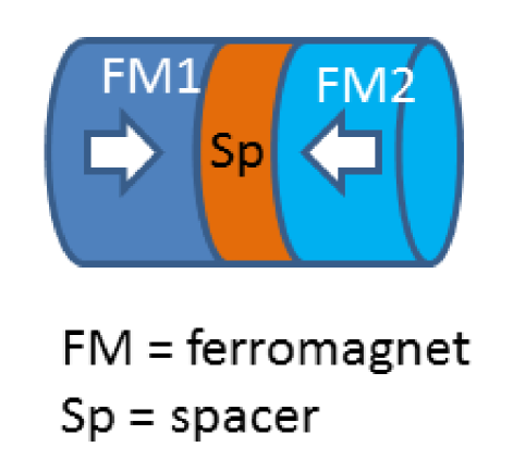
Consider a tri-layered nanowire spin-valve as shown in Fig. 1 whose two ferromagnetic contacts have opposite signs of tunneling spin-polarization. They could be made of Co and Fe. Applying a strong magnetic field along the nanowire axis magnetizes both contacts in the direction of the field. Spins parallel to the magnetic field will become majority spins in the contacts while those anti-parallel will become minority spins. Assume that the left contact is Co and the right contact is Fe. Under a suitable bias, the left contact preferentially injects its minority spins into the middle spacer layer via tunneling through the Schottky barrier at the Co/spacer interface since Co has a negative tunneling spin polarization at the Fermi energy [22]. These spins cannot transmit easily through the Schottky barrier at the right contact interface into the Fe contact since they are minority spins and Fe has a positive tunneling spin polarization [22]. However, if the injected spins flip (relax) in transit, then they will become majority spins at the right contact and transmit easily [23]. If the spin relaxation rate can be increased with IR light, then that will increase the likelihood of the injected spins flipping and thereafter being transmitted easily by the right contact. This will cause an increase in the current through the nanowire under IR illumination, which is the physical basis of the photodetection mechanism. We can estimate the light-to-dark current contrast ratio of the photodetector as follows:
Assume that IR light induces only intra-band transitions in the conduction band of the spin-valve’s spacer layer and not inter-band transitions from the valence to the conduction band which would have changed the carrier concentration. This assumption would be particularly true for wide-gap semiconductor spacers where the bandgap vastly exceeds the IR photon energy. Also assume that the current in the spacer is mostly due to drift and not diffusion. In that case, it is given by
| (1) |
where is the electron charge, is the drift velocity of electrons, is the linear electron concentration in the spacer layer, is the length of the spacer layer, is the spin injection efficiency at the injecting (left) contact, is the spin detection efficiency at the detecting (right) contact, and is the spin relaxation length in the spacer layer, ensemble averaged over electron velocity.
In deriving the above relation, we made two assumptions. First, even in single subband transport (when DP relaxation is absent), spin-orbit interaction will make the spins precess as they travel, but the angle by which they precess in traversing the distance is the same for all electrons (coherent rotation) [3]. We neglected this precession since is very small when is small. Second, in multi-subband transport when DP relaxation is present, different electrons will precess by different amounts in traversing the distance (incoherent rotation) which causes spin relaxation in space and is the basis of DP relaxation. We assume that this relaxation is captured by an exponential decay of spin polarization with distance. This, however, may be only approximately true [24].
Assuming that IR light does not change or appreciably, the light-to-dark contrast ratio will be
| (2) |
where and are the spin relaxation lengths under illumination and in the dark, respectively. In the event , the above expression simplifies to
| (3) | |||||
Experimental details
In order to demonstrate modulation of the DP spin relaxation rate with IR light and additionally to lay the foundation for a spintronic IR photodetector, we fabricated arrays of Co-InSb-Ni nanowires of 50 nm diameter. First, nanoporous anodic alumina films, containing parallel arrays of 50-nm diameter cylindrical nanopores, were produced by anodizing 99.999% pure aluminum foils in 0.3M oxalic acid at room temperature. Prior to anodization, the foils were electropolished in a solution of perchloric acid, butyl cellusolve, ethanol and distilled water to reduce the surface roughness to 3 nm [25]. The anodization was carried out at 40 V dc for 15 minutes; the voltage was then gradually reduced to 15 V at the rate of 0.1 V/sec and held for 10 minutes before terminating the anodization abruptly. This step anodization process [26] allows us to remove the thin alumina layer that forms at the bottom of the pores (which is a barrier to dc current flow) by later soaking the porous film in 5% phosphoric acid for 30 minutes.
After removal of the barrier layer, cobalt is dc-electrodeposited selectively within the pores from a solution of 28.09 gm of CoSO47H2O and 7 gm of boric acid dissolved in 1 liter of distilled water. Next, InSb is dc-electrodeposited from a solution of 0.15M InSO4, 0.1M SbCl3, 0.17M Na3C6H5O7 and 0.36M C6H8O7 (citric acid) dissolved in 250 ml of distilled water [27]. Finally, Ni is dc-electrodeposited from a solution of 26.27 gm of NiSO46H2O and 7 gm of boric acid dissolved in 1 liter of distilled water. The Co and InSb depositions are carried out at 3 V dc for 30 seconds and 1 minute, respectively, while the Ni deposition is carried out at 5 V dc for 4 minutes to fill the pores to the brim or slightly overfill and make Ni spill out on the surface. A 50-nm thick layer of Ni is then electron-beam-evaporated on the surface through a mask. The nanowires are electrically contacted from the top and bottom with copper wires attached to the top surface (evaporated Ni) and the bottom aluminum substrate with silver paste. Since the nanowire density is 1010 cm-2 and the contact area is a circle of roughly 6 mm diameter, about 3109 wires are contacted in parallel and probed in electrical measurements.
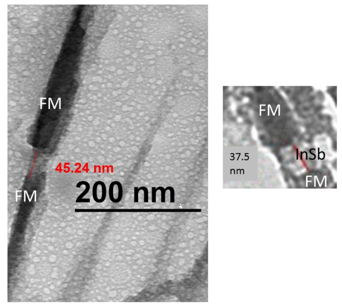
Fig. 2 shows transmission electron micrographs (TEM) of isolated nanowire spin valves. The TEM samples were prepared by dissolving out the porous alumina matrix hosting the nanowires in dilute NaOH and then capturing the released wires on TEM grids by soaking the grids in the solution. Since Co and Ni both have atomic densities of roughly 9.11022 cm-3, while InSb has an atomic density of 2.941022 cm-3, the InSb region appears more transparent than the Co or Ni regions in a bright field TEM image.
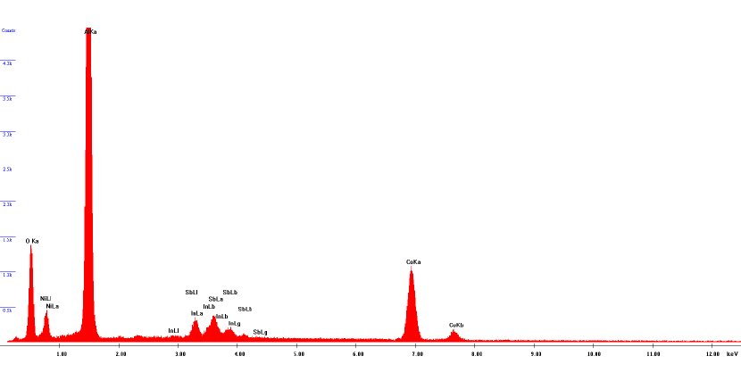
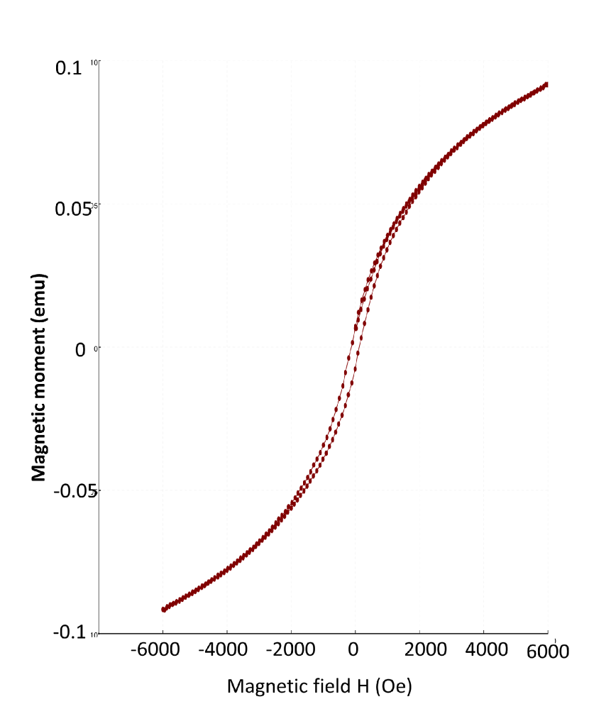
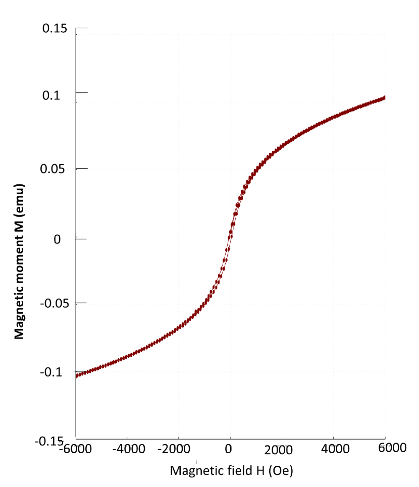
Energy dispersive x-ray spectroscopy (EDS) of the nanowire spin valves nestled within the alumina matrix is presented in the supplementary material. We found clear peaks due to Ni, Co, In and Sb (associated with the nanowire spin valves), as well as Al and O peaks caused by the alumina matrix and the aluminum substrate. The magnetization curves for porous alumina samples filled with just Co (30 seconds electrodeposition) and just Ni (4 minutes electrodeposition) are shown in the supplementary material and confirm that the nanocontacts are ferromagnetic and have non-zero remanence, albeit with small coercivity. The single subband occupancy of the nanowires (in the dark) was established in Ref. [16].
Results and Discussion
Since the Ni electrodeposition is carried out for a relatively long duration, the Ni nanocontacts have cylindrical shapes conforming to the pores in which they are produced and their axes are collinear with the nanowires’ common axis. Therefore, their easy axes of magnetization is always along the wire axis. However, since the Co deposition is carried out for only 30 seconds, the Co layers in the spin valves are very short and therefore do not necessarily have cylindrical shapes with their easy axes of magnetization along the nanowire axis. Consequently, their magnetizations may not be collinear with the nanowires’ common axis when no magnetic field is present. At a high enough magnetic field directed along the wire axis, the magnetizations of the short Co contacts will ultimately rotate to align along the field and hence along the nanowire axis. For each nanocontact, this will happen abruptly when the magnetostatic energy due to the magnetic field just overcomes its shape anisotropy energy barrier. If the shape anisotropy energy barrier does not vary too much from one Co nanocontact to another among the 3109 nanowires probed, then all nanocontacts undergo the rotation at nearly the same field. At that threshold field, the majority spins in the Co and Ni contacts should suddenly become parallel, and the (spin-dependent) transmission probability of the electrons should jump, causing the resistance of the entire sample (consisting of 3109 nanowires in parallel) to drop abruptly at that field. On the other hand, if the shape anisotropy energy barriers vary significantly from one Co nanocontact to another, then different nanocontacts in a sample will rotate at different fields and the resistance of the sample should drop gradually with increasing field and not abruptly. However, in some circumstances, a very different behavior may be observed, depending on the nature of the transport in the InSb layer. If there is a point defect site in the InSb spacer layer close to one of the ferromagnetic electrodes and this defect has an energy level that is resonant with the Fermi energy of that electrode, then an electron traversing the spacer layer will resonantly tunnel through this defect site and that will effectively invert the spin polarization of that ferromagnetic electrode [28]. In that case, the resistance of the spin valve will rise at the threshold field instead of dropping. This type of polarization inversion has been frequently observed in ferromagnetic/paramagnetic nanojunctions of cross section smaller than 0.01 m2 grown by electrodeposition, as is the case here [28]. Therefore, if resonant tunneling occurs, then we will expect a rise in the spin valve resistance (either abrupt or gradual) with increasing magnetic field, whereas if no such tunneling occurs, then we will expect a drop. The sign of the magnetoresistance change therefore depends on the nature of transport. Both signs have been observed in different samples fabricated in the same run in the past because the impurity characteristics are beyond control [29]. We too have observed both signs in our samples.
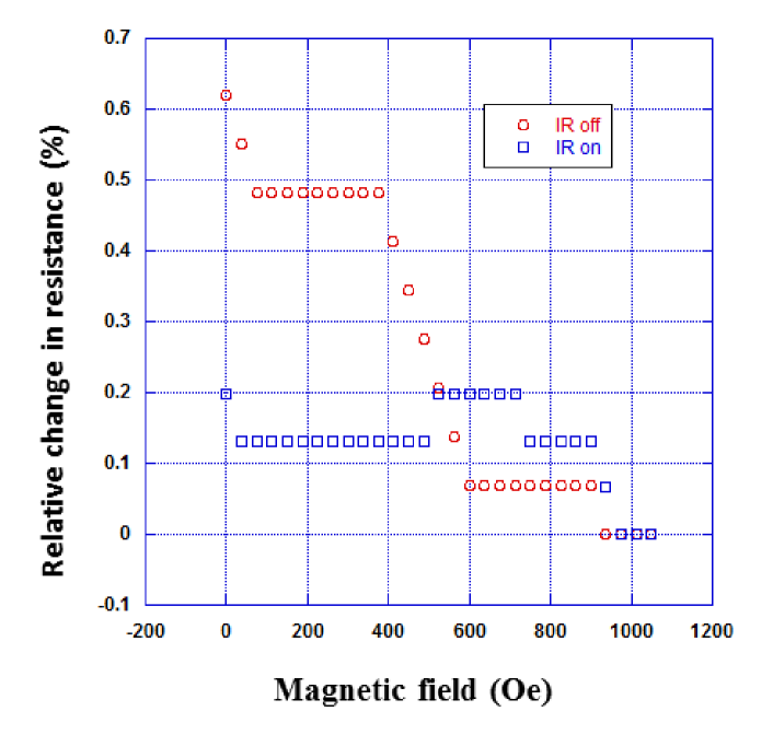
In Fig 3, we show the room-temperature magnetoresistance of one sample measured in the dark and under illumination by an infrared (IR) lamp radiating in the wavelength range 2-5 m. The magnetoresistance was measured with the magnetic field directed parallel to the axes of the wires. The lamp was kept far enough away from the sample to avoid heating effects. The resistance was monitored as a function of time during illumination to see if it drifted with time. Since no drift was observed, there are no discernible thermal effects on resistance due to the IR lamp.
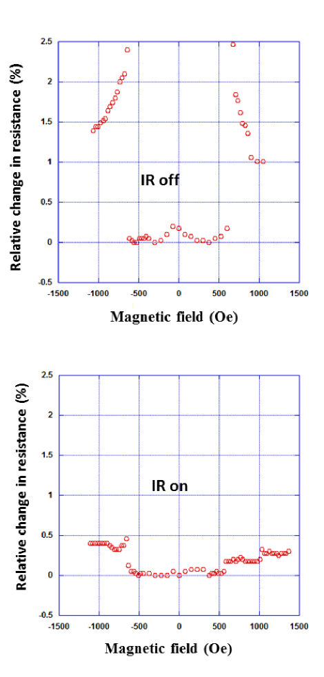
The data taken in the dark (top panel of Fig. 3) show a reproducible abrupt jump in the resistance by 2.5% when the magnetic field strength exceeds 650 Oe. Clearly, this is the threshold field at which the magnetizations of the Co nanocontacts overcome their shape anisotropy energy barriers and rotate to align along the nanowire axis. The fact that the resistance rise is abrupt indicates that the variation in the shape anisotropy energy barrier among the different Co nanocontacts in this sample is small.
Note that beyond the threshold field, the resistance actually drops continuously. This is probably due to the fact that the magnetic field increases the energy separation between subbands and decreases inter-subband scattering in the InSb spacer layers, thereby slightly decreasing the resistance. This is unrelated to any spin-sensitive effect. However, the continuous decrease in magnetoresistance beyond the threshold field gives us additional confidence that the sudden step increase at the threshold field must be due to spin-polarized transport.
When the magnetoresistance is measured under constant IR illumination (bottom panel of Fig. 3), we observe the same resistance jump at around 650 Oe magnetic field, but this time the resistance change is only 0.4%, which is considerably less than that in the dark. The more than 6-fold decrease in the step can only happen if spin-polarized transport has been weakened by IR light. The IR light causes multi-subband transport in the InSb spacer layers of the spin valves by exciting electrons to the higher subbands and therefore shortens the spin relaxation length by reviving DP relaxation. The shorter spin relaxation length decreases spin polarization of the current and hence suppresses the step increase in the magnetoresistance at the threshold field.
We can obtain at least an order estimate for the average spin relaxation length in the InSb spacer layers – both in the dark and under IR illumination – from the modified Jullieré formula for drift transport [30, 31]:
| (4) |
where is the relative change in resistance at the step, are the spin polarizations of the two contacts, is the average width of the InSb layer and is the average spin relaxation length. The TEM results in Fig. 2 show 40 nm. Because the Co nanocontacts are small, but the common Ni contact to the nanowires is large (6 mm diameter) and approximates bulk, we will assume = 0.1 (for Co) [16, 32] and = 0.33 (for Ni) [22]. Therefore, from the measured , we get 40 nm in this sample at room temperature in the dark. Under IR illumination, the quantity drops to 0.4% from 2.5%, indicating that the average spin relaxation length has decreased three-fold to 14 nm. Therefore, = 40 nm and = 14 nm.
It is reasonable to assume that and . If we use the values = 0.1, = 0.33, = 40 nm, = 40 nm and = 14 nm in Equation (2) to find the relative change in resistance between dark and illuminated conditions, we find that the quantity = 2%, where is the dark resistance and is the resistance under illumination. Experimentally, we measure this quantity to be also 2% (see Fig 3), which indicates excellent agreement between theory and experiment.
In Fig. 4, we show the magnetoresistance of another sample measured in the dark and under IR illumination. In the dark, this sample shows a more gradual resistance drop in the magnetic field range 400 Oe - 600 Oe – more gradual probably because there is significant variation in the shape anisotropy energy barriers among the Co nanocontacts. The fact that the resistance decreases with increasing magnetic field indicates that the carriers in this sample transport without resonantly tunneling through defect sites. The majority spins in the two magnetic nanocontacts begin to become parallel when the magnetic field exceeds 400 Oe, resulting in the gradual resistance drop. The drop is 0.4%. Under illumination, there is no discernible change in the resistance with increasing magnetic field (the random jumps of 0.1% change show no systematic trend), indicating that no significant spin-polarized transport is taking place since the average spin relaxation length has become much shorter than the average spacer layer length. In this sample too, light had induced multi-subband transport, thereby reviving the DP relaxation and shortening the average spin relaxation length. Equation (4) yields that the spin relaxation length in this sample is 14 nm in the dark and immeasurably small under illumination. These results are summarized in Table I.
| (dark) | (illuminated) | |
|---|---|---|
| Sample 1 | 40 nm | 14 nm |
| Sample 2 | 14 nm | Immeasurably small |
There have been previous reports of modulating the spin relaxation time and length in semiconductor quantum wells by modulating the Rashba spin-orbit interaction strength with an external electric field applied via a gate [33, 34]. However, the mechanism there is different; spin relaxation time and length are not controlled by changing subband occupation, but by changing the strength of the relaxation source, namely the spin-orbit interaction strength. This may have transistor applications [23], whereas the present effect has photodetector applications.
The IR source is a broadband lamp and radiates in the wavelength range between 2 and 5 m corresponding to photon energies between 9.4 kT and 24 kT, while the effective bandgap of the InSb layer is 6.5 kT. Therefore, the IR illumination will induce both inter-band transition (valence-to-conduction band) and inter-subband transition within the conduction band of the InSb spacer layer. The resistance of the sample at zero magnetic field (when significant spin-polarized transport does not occur) however decreased by only 0.15% under illumination indicating that the inter-band transition (which will increase the electron and hole population in the InSb spacer and therefore decrease the resistance) is not significant. This is because the light intensity from the IR lamp is too weak for significant interband transitions to occur. It is therefore also too weak to cause significant intraband (or inter-subband) transitions, and yet the spin relaxation length decreased by a factor of three under illumination. This is due to the fact that even a slight departure from single subband transport can increase the DP relaxation rate considerably and quench spin-polarized transport. It is an encouraging observation since it portends high detectivity and small noise equivalent power for photodetectors predicated on this effect.
Conclusion
In this work, we have shown that it is possible to modulate the spin relaxation rate in a nanowire with light by controlling the D’yakonov-Perel’ mechanism. The mechanism is suppressed in the dark owing to near single subband occupancy and revived under illumination as more subbands get populated by photoexcitation.
If the spin injection and detection efficiencies in these spin valves can be improved, and the Elliott-Yafet and other spin relaxation mechanisms suppressed by producing very high mobility samples with weak hyperfine interactions, then we can use this effect to implement a room-temperature IR detector with very high light-to-dark contrast ratio. Consider the situation when the spin injection/detection efficiencies approach 100%. From Equation (3), we get that the contrast ratio is , where is the DP relaxation length in single-subband transport (infinity) and is the DP relaxation length in multi-subband transport (finite). Such a photodetector will also ideally have nearly zero dark current and hence almost zero standby power dissipation, making it very attractive. The experiments reported here lay the groundwork for such a device.
Acknowledgement
The work at Virginia Commonwealth University is supported by the US National Science Foundation under grant CMMI-1301013.
References
- [1] M. I. D’yakonov and V. I. Perel’ 1971 Spin orientation of electrons associated with the interband absorption of light in semiconductors Sov. Phys. JETP 33 1053.
- [2] S. Pramanik, S. Bandyopadhyay and M. Cahay 2005 Spin relaxation in the channel of a spin field-effect transistor IEEE Trans. Nanotechnol. 4 2.
- [3] S. Bandyopadhyay and M. Cahay 2008 Introduction to Spintronics (CRC Press, Boca Raton).
- [4] Y. A. Bychkov and E. I. Rashba 1984 Oscillatory effects and the magnetic susceptibility of carriers in inversion layers J. Phys. C: Solid State Phys. 17 6039.
- [5] G. Dresselhaus 1955 Spin-orbit coupling effects in zinc-blende structures Phys. Rev. 100 580.
- [6] M. I. D’yakonov and V. I. Perel’ 1972 Spin relaxation of conduction electrons in non-centrosymmetric semiconductors Sov. Phys. Solid State 13 3023.
- [7] N. S. Averkiev and L. E. Golub 1999 Giant spin relaxation anisotropy in zinc-blende heterostructures Phys. Rev. B 60 15582.
- [8] N. S. Averkiev, L. E. Golub and M. Willander 2002 Spin realxation anisotropy in two-dimensional semiconductor systems J. Phys: Condens. Matt. 14 R271.
- [9] J. Kainz, U. Rössler and R. Winkler 2003 Anisotropic spin splitting and spin relaxation in asymmetric zinc-blende semiconductor quantum structures Phys. Rev. B 68 075322.
- [10] P. H. Song and K. W. Kim 2002 Spin relaxation of conduction electrons in bulk III-V semiconductors Phys. Rev. B 66 035207.
- [11] S. Patibandla, G. M. Atkinson, S. Bandyopadhyay and G. C. Tepper 2010 Competing D’yakonov-Perel’ and Elliott-Yafet spin relaxation in germanium Physica E 42 1721.
- [12] A. Bournel, P. Dollfus, P. Bruno and P. Hesto 1998 Gate-induced spin precession in an In0.53Ga0.47As two-dimensional electron gas Eur. Phys. J. Appl. Phys. 4 1.
- [13] A. G. Mal’shukov and K. A. Chao 2000 Waveguide diffusion modes and slowdown of D’yakonov-Perel’ spin relaxation in narrow two-dimensional semiconductor channels Phys. Rev. B 2000, 61, R2413.
- [14] A. A. Kiselev and K. W. Kim 2000 Progressive suppression of spin relaxation in two-dimensional channels of finite width Phys. Rev. B 61 13115.
- [15] T. P. Pareek and P. Bruno 2002 Spin coherence in a two-dimensional electron gas with Rashba spin-orbit interaction Phys. Rev. B 65, 241305(R).
- [16] S. Bandyopadhyay, Md. I. Hossain, H. Ahmad, J. Atulasimha and S. Bandyopadhyay 2014 Coherent spin transport and suppression of spin relaxation in InSb nanowires with single subband occupancy at room temperature Small 10 4379. Please see the supplementary material accompanying this paper for exhaustive thereotical analyses and characterization of the InSb self-assembled nanowires.
- [17] A. W. Holleitner, V. Sih, R. C. Myers, A. C. Gossard and D. D. Awschalom 2006 Suppression of spin relaxation in submicron InGaAs wires Phys. Rev. Lett. 97 036805.
- [18] B. J. Van Wees 1988 Quantized conductance of point contacts in a two-dimensional electron gas Phys. Rev. Lett. 60 848.
- [19] D. A. Wharam, et al. 1988 One dimensional transport and the quantization of ballistic resistance J. Phys.C - Solid St. Phys. 21 L209.
- [20] R. J. Elliott 1954 Theory of the effect of spin-orbit coupling on magnetic resonance in some semiconductors Phys. Rev. 96 266.
- [21] P. Upadhyaya, S. Pramanik and S. Bandyopadhyay 2008 Optical transitions in a quantum wire with spin-orbit interaction and its application in terahertz electronics: Beyond zeroth-order theory Phys. Rev. B 77 155439.
- [22] E. Y. Tsymbal, O. N. Mryasov and P. R. Leclair 2003 Spin dependent tunneling in magnetic tunnel junctions J. Phys: Condens. Matt. 15 R109.
- [23] K. C. Hall and M. E. Flatté 2006 Performance of a spin-based insulated gate field effect transistor Appl. Phys. Lett. 88 162503.
- [24] S. Pramanik, S. Bandyopadhyay and M. Cahay 2004 Decay of spin-polarized hot carrier current in a quasi one-dimensional spin-valve structure Appl. Phys. Lett. 84 266.
- [25] S. Bandyopadhyay, et al. 1996 Electrochemically assembled quasi periodic quantum dot arrays Nanotechnology 7 360.
- [26] R. C. Furneaux, W. R. Rigby and A. P. Davidson 1989 The formation of controlled porosity membranes from anodically oxidized aluminium Nature 337 147.
- [27] X. Zhang, Y. Hou, G. Meng and L. Zhang 2005 Fabrication of highly ordered InSb nanowire arrays by electrodeposition in porous anodic alumina membranes J. Electrochem. Soc. 152 C664.
- [28] E. Y. Tsymbal, A. Sokolov, I. F. Sabirianov and B. Doudin 2003 Resonant inversion of tunneling magnetoresistance Phys. Rev. Lett. 90 186602.
- [29] S. Pramanik, S. Bandyopadhyay, K. Garre and M. Cahay 2006 Normal and inverse spin-valve effect in organic semiconductor nanowires and the background monotonic magnetoresistance Phys. Rev. B. 74 235329.
- [30] M. Jullieré 1975 Tunneling between ferromagnetic films Phys. Lett. A 54 225.
- [31] Z. H. Xiong, D. Wu, Z. V. Vardeny and J. Shi 2004 Giant magnetoresistance in organic spin valves Nature 427 821.
- [32] S. O. Valenzuela and M. Tinkham 2004 Spin-polarized tunneling in room-temperature mesoscopic spin valves Appl. Phys. Lett. 85 5914.
- [33] S. Iba, S. Koh and H. Kawaguchi 2010 Room temperature gate modulation of electron spin relaxation time in (110)-oriented GaAs/AlGaAs quantum wells Appl. Phys. Lett. 97 202102.
- [34] G. Wang, et al. 2013 Gate control of the electron spin-diffusion length in semiconductor quantum wells Nature Commun. 4, 2372.
1 SUPPLEMENTARY MATERIAL
Numerous theoretical analyses and characterization results are presented in ref. [16] of the main paper and the associated supplementary material which are not repeated here. They are to be viewed in conjunction with the material here.
We provide here energy-dispersive x-ray spectra of nanowire spin-valve samples used in the experiments [Fig. 5], as well as room-temperature magnetization (M-H curves) results of Co and Ni electrodeposited in nanoporous alimina hosts for 30 seconds and 4 minutes, respectively [Figs. 6 and 7]. The M-H curves were obtained with a Quantum Design Vibrating Sample Magnetometer.
2 Transport model
The resonant tunneling through defect sites that results in inversion of the spin valve resistance peak [discussed in the main paper and ref. [28]] does not require electrons to tunnel resonantly through the entire spacer layer; instead it requires resonant tunneling through one or more defect sites (approximated as “point defects”) that are much smaller in physical extent than the spacer layer. If we draw the conduction band profile of the spacer layer, it will look like the diagram in Fig. 8. As long as there is a point defect close to a contact and electrons resonantly tunnel through it, the sign of the contact’s spin polarization will be inverted. If there is no such point defect then the sign will not be inverted. That is why one sample showed sign inversion and another did not.
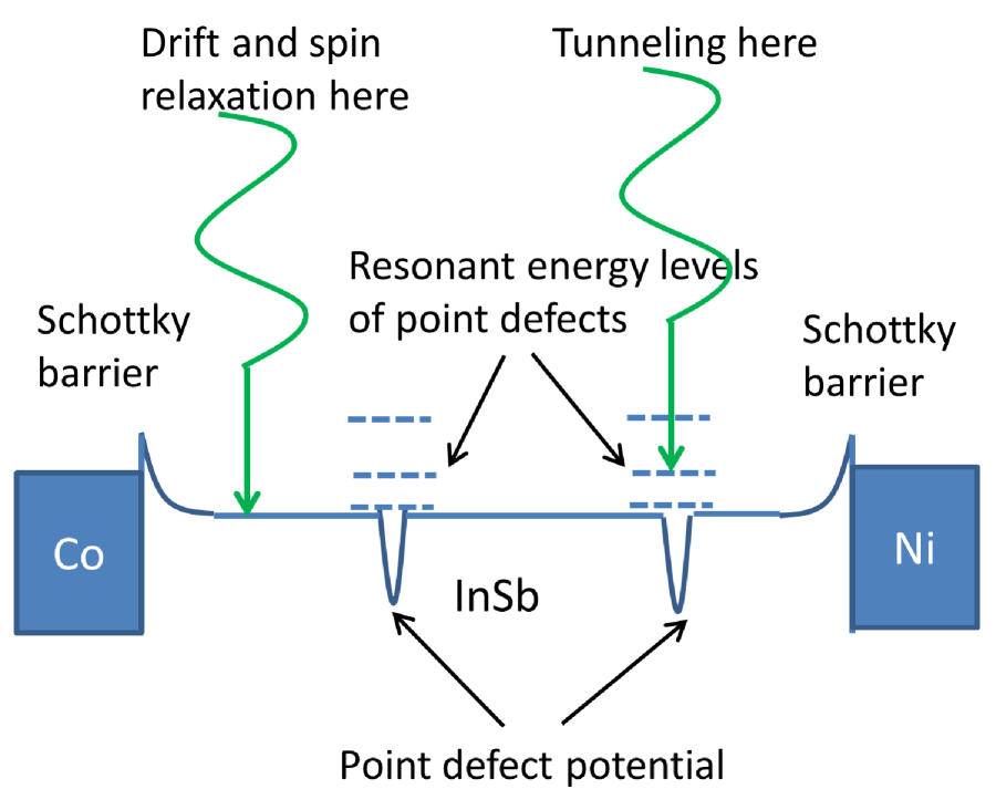
Spin relaxation occurs during carrier drift between successive defect sites. Single subband occupancy reduces the associated relaxation rate by eliminating DP relaxation.
3 The threshold magnetic field
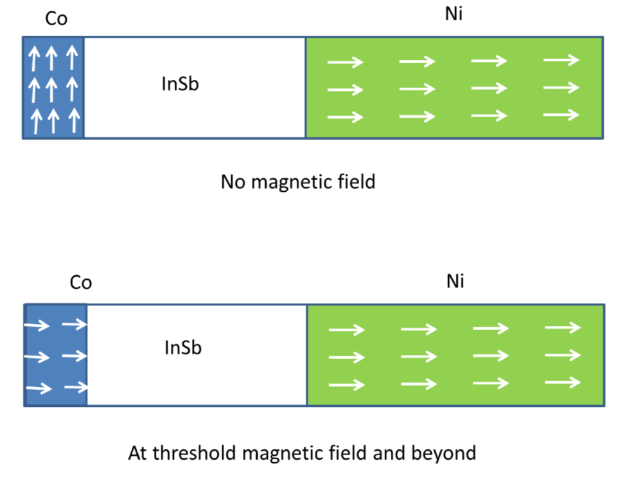
In the absence of any magnetic field, the Co contact’s easy axis of magnetization is not along the pore axis, but perpendicular to it, as shown in the top panel of Fig. 9 because the thickness of the cobalt layer within the pore is smaller than the pore diameter of 50 nm. The Co contact is roughly a cylinder of circular cross section whose cross-sectional diameter is 50 nm and height is much smaller than 50 nm. This happens because the Co layer is electrodeposited within the pore for a very short duration intentionally (our electrodepostion calibration predicts that the Co layer thickness will be around 20 nm). Hence, the Co layer s easy axis of magnetization will be in the plane perpendicular to the pore axis and the magnetization of the Co contact will be stable only in that plane. In other words, the Co contact’s magnetization in the absence of an external magnetic field will be pointing perpendicular (or nearly perpendicular) to the pore axis as shown in the top panel of the figure below.
A certain amount of external magnetic field will therefore be required to turn the magnetization of the Co contact by 90∘ and make it point along the pore axis so that it can inject/detect electrons whose spins are polarized along the pore axis. This magnetic field is the one required to overcome the Co contact’s shape anisotropy energy barrier and make its magnetization point along the cylinder s axis as shown in the bottom panel of Fig. S5. This is the threshold field at which the magnetoresistance jumps because at or beyond this field, the Co contact preferentially injects spins polarized along the pore axis, which are blocked by the Ni contact since its polarization is also along the pore axis but effectively inverted owing to resonant tunneling through the defect sites in the InSb spacer.
