Boosting Domain Wall Propagation by Notches
Abstract
We report a counter-intuitive finding that notches in an otherwise homogeneous magnetic nanowire can boost current-induced domain wall (DW) propagation. DW motion in notch-modulated wires can be classified into three phases: 1) A DW is pinned around a notch when the current density is below the depinning current density. 2) DW propagation velocity is boosted by notches above the depinning current density and when non-adiabatic spin-transfer torque strength is smaller than the Gilbert damping constant . The boost can be manyfold. 3) DW propagation velocity is hindered when . The results are explained by using the Thiele equation.
pacs:
75.60.Ch, 75.78.-n, 85.70.Ay, 85.70.KhI Introduction
Magnetic domain wall (DW) motion along a nanowire underpins many proposals of spintronic devices [1, 2]. High DW propagation velocity is obviously important because it determines the device speed. In current-driven DW propagation, many efforts have been devoted to high DW velocity and low current density in order to optimize device performance. The issue of whether notches can enhance current-induced DW propagation is investigated here.
Traditionally, notches are used to locate DW positions [1, 2, 3, 4]. Common wisdom expects notches to strengthen DW pinning and to hinder DW motion. Indeed, in the field-driven DW propagation, intentionally created roughness slows down DW propagation although they can increase the Walker breakdown field [5]. Unlike the energy-dissipation mechanism of field-induced DW motion [6], spin-transfer torque (STT) [7, 8, 9, 10] is the driven force behind the current-driven DW motion. The torque consists of an adiabatic STT and a much smaller non-adiabatic STT [9, 10]. In the absence of the non-adiabatic STT, there exists an intrinsic pinning even in a homogeneous wire, below which a sustainable DW motion is not possible [11, 12]. Interestingly, there are indications [13] that the depinning current density of a DW trapped in a notch is smaller than the intrinsic threshold current density in the absence of the non-adiabatic STT. Although there is no intrinsic pinning [10, 1] in the presence of a non-adiabatic STT, It is interesting to ask whether notches can boost DW propagation in the presence of both adiabatic STT and non-adiabatic STT.
In this paper, we numerically study how DW propagates along notch-modulated nanowires. Three phases are identified: pinning phase when current density is below depinning current density ; boosting phase and hindering phase when the current density is above and the non-adiabatic STT strength is smaller or larger than the Gilbert damping constant , respectively. The average DW velocity in boosting and hindering phases is respectively higher and lower than that in the wire without notches. It is found that DW depinning is facilitated by antivortex nucleation. In the case of , the antivortex generation is responsible for velocity boost because vortices move faster than transverse walls. In the other case of , the longitudinal velocity of a vortex/antivortex is slower than that of a transverse wall in a homogeneous wall and notches hinder DW propagation.
II Model and Method
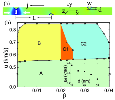
We consider sufficient long wires (with at least 8 notches) of various thickness and width. It is well known that [14] narrow wires favor only transverse walls while wide wires prefer vortex walls. Transverse walls are the main subjects of this study. A series of identical triangular notches of depth and width are placed evenly and alternately on the two sides of the nanowires as shown in Fig. 1a with a typical clockwise transverse wall pinned at the center of the first notch. The , and axis are along length, width, and thickness directions, respectively. The magnetization dynamics of the wire is governed by the Landau-Lifshitz-Gilbert (LLG) equation
where , , , and are respectively the unit vector of local magnetization, the gyromagnetic ratio, the effective field including exchange and anisotropy fields, and the Gilbert damping constant. The third and fourth terms on the right hand side are the adiabatic STT and non-adiabatic STT [10]. The vector is along the electron flow direction and its magnitude is , where , , , , and are current density, current polarization, the Bohr magneton, the electron charge and the saturation magnetization, respectively. For permalloy of A/m, m/s corresponds to . In this study, is limited to be smaller than both 850 m/s (corresponding to !) and the Walker breakdown current density because current density above the values generates intensive spin waves around DWs and notches, which makes DW motion too complicated to be even described. Dimensionless quantity measures the strength of non-adiabatic STT and whether is larger or smaller than is still in debate [10, 15, 16]. The LLG equation is numerically solved by both OOMMF [17] and MUMAX [18] packages [19]. The electric current density is modulated according to wire cross section area while the possible change of current direction around notch is neglected. The material parameters are chosen to mimic permalloy with exchange stiffness J/m, and varying from to . The mesh size is .
III Results
III.1 Transverse walls in wide wires: boosting and hindering
This is the focus of this work. Our simulations on wires of 4 nm thick and width ranging from 32 nm to 128 nm and notches of nm and varying from 16 nm to 128 nm show similar behaviors. Domain walls in these wires are transverse. Results presented below are on a wire of 64 nm wide and notches of nm. Three phases can be identified. A DW is pinned at a notch when is below a depinning current density . This pinning phase is denoted as A (green region) in Fig. 1b. Surprisingly, increases slightly with , indicating that the -term actually hinders DW depinning out of a notch although it is responsible for the absence of the intrinsic pinning in a uniform wire (see discussion below for possible cause). When is above , a DW starts to propagate and it can either be faster or slower than the DW velocity in the corresponding uniform wire, depending on relative values of and .
When , DW velocity is boosted through antivortex generation at notches. This phase is denoted as phase B. When , the boosting of DW propagation is suppressed no matter vortices are generated (phase C1) or not (phase C2). The upper bound of the phase plane is determined by the Walker breakdown current density and m/s. If the current density is larger than the upper bound, spin waves emission from DW [20] and notches are so strong that new DWs may be created. Also, the Walker breakdown is smaller than the depinning value for . Thus the phase plane in Fig. 1b is bounded by . Although the general phase diagram does not change, the phase boundaries depend on the wire and notch specificities. The inset is notch depth dependence of the depinning current when nm and [21].
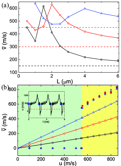
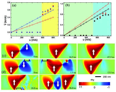
Boosting phase: The boost of DW propagation for can be clearly seen in Fig. 2. Figure 2a is the average DW velocity as a function of notch separation for m/s . is maximal around an optimal notch separation , which is close to the longitudinal distance that an antivortex travels in its lifetime. increases with and it is respectively about 1.5 m, 2 m, and 4 m for (squares), 0.01 (circles) and 0.015 (up-triangles). This result suggests that the antivortex generation and vortex dynamics are responsible for the DW propagation boost. Filled symbols in Fig. 2b are for various current density when is used. For a comparison, DW velocities in the corresponding homogeneous wires are also plotted as open symbols which agree perfectly with discussed below. Take as an example, is zero below m/s and jumps to an average velocity m/s at , which is about four times of the DW velocity in the homogeneous wire. As the current density further increases, the average velocity also increases and is approximately equal to . The inset of Fig. 2b shows the instantaneous DW velocity for and m/s. Blue dots denote the moments at which the DW is at notches. Right after the current is turned on at ns, the instantaneous DW velocity is very low until an antivortex of winding number [23, 24] is generated near the notch edge at 0.5 ns (see discussion and Fig. 9 below). The motion of the antivortex core drags the whole DW to propagate forward at a velocity around 600 m/s. The antivortex core annihilates itself at the bottom edge of the wire after traveling about 1.5 m and the initial transverse wall reverses its chirality at the same time [24]. Surprisingly, the reversal of DW chirality leads to a significant increases of DW velocity as shown by the peaks of the instantaneous velocity at about 2.0ns in the inset. Another antivortex of winding number is generated at the second notch and DW propagation speeds up again. Once the antivortex core forms, it pulls the DW out of notch. This process then repeats itself and the DW propagates at an average longitudinal velocity of about 600 m/s. A supplemental movie corresponding to the inset is attached [25].
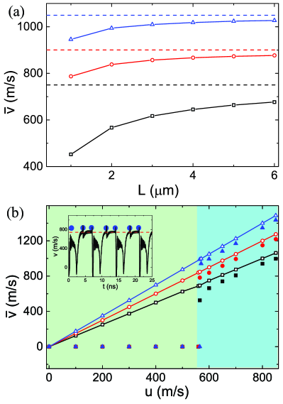
Hindering phase: Things are quite different for . Figure 3a shows that increases monotonically with for , 0.03 and 0.035, which are all larger than . In order to make a fair comparison with the results of , Fig. 3b is the current density dependence of for m and (filled squares), 0.03 (filled circles) and 0.035 (filled up-triangles). Again, DW velocities in the corresponding homogeneous wires are presented as open symbols. Take as an example, although the average velocity jumps at the depinning current density 565 m/s, it’s still well below the DW velocity in the corresponding uniform wire. The inset of Fig. 3b shows the instantaneous DW velocity for m/s. An antivortex is generated at the first notch. In contrast to the case of , the antivortex slows down DW propagation velocity below the value in the corresponding uniform wire. Moreover, the transverse wall keeps its original chirality unchanged when the antivortex is annihilated at wire edge, and no vortex/antivortex is generated at the second notch. However, another antivortex is generated at the third notch. This is the typical cycle of phase C1. As increases above 640 m/s, phase C1 disappears and the DW passes all the notches without generating any vortices. This motion is termed as phase C2. For , only phase C2 is observed. In C2, DW profile is not altered, and the average DW velocity is slightly below that in a uniform wire.
III.2 Transverse walls in very narrow wires
One interesting question is whether notches can boost DW propagation in very narrow wires such that the nucleation of a vortex/antivortex is highly unfavorable. To address this issue, Fig. 4a are dependence of the average DW velocity on a 8 nm wide wire for (circles for and up-triangles for ) with (filled symbols) and without (open symbols) notches. When notches are placed, notch depth is 2 nm, nm, nm. DW velocity in the corresponding homogeneous wire (open symbols) follows perfectly with (straight lines). It is clear that averaged DW velocity in the notched wire (filled symbols) is below the values of the DW velocity in the corresponding homogeneous wire. Take as an example, is zero below m/s and jumps to an average velocity m/s at , which is below the DW velocity in the corresponding uniform wire.
Things are similar for . Figure 4b is the current density dependence of for (filled squares) and 0.035 (filled up-triangles). Again, DW velocities in homogeneous wire are presented as open symbols for a comparison. The averaged DW velocity in the notched wire (filled symbols) is below the values of the DW velocity in the corresponding homogeneous wire.
III.3 Vortex walls in very wide wires
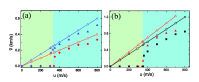
Although our main focus is on transverse walls, it should be interesting to ask whether DW propagation boost can occur for vortex walls. It is well-known that a vortex/antivortex wall is more stable for a much wider wire in the absence of a field and a current [14]. One may expect that DW propagation boost would not occur in such a wire because the boost comes from vortex/antivortex generation near notches and a such vortex/antivortex exists already in a wider wire even in the absence of a current. However, DW propagation boost was still observed as shown in Fig. 5 for a wire of 520 nm wide and 10 nm thick. Rectangular notches of 60 nm deep and 160 nm wide are separated by m. When (Fig. 5a: circles for and up-triangles for ), the average DW propagation velocities in the notched wire (filled symbols) is higher than the DW velocity in the corresponding homogeneous wire (open symbols) when . Figure 5b shows that the average DW propagation velocities in a notched wire (filled symbols) is lower than that in the corresponding homogeneous wire (open symbols) for (squares for and circles for ). Figure 5c shows the spin configurations of the DW in the homogeneous wire of before a current is applied (the left configuration) and during the current-driven propagation (middle and right configurations). When a current m/s is applied at 0 ns, a vortex wall moves downward. The vortex was annihilated at wire edge, and the vortex wall transform into a transverse wall. The DW keeps its transverse wall profile and propagates with velocity of (solid lines in Fig. 5a and 5b). The middle and right configurations are two snapshots at 14.5 ns and 47.5 ns. Time is indicated in the bottom-right corner. Figure 5d are snapshots of DW spin configurations in the notched wire of when a current m/s is applied at ns. At ns, a vortex wall is pinned near the first notch. Right after the current is turned on, the vortex wall starts to depin and complicated structures may appear during the depinning process as shown by the snapshot at ns. At ns, the DW transforms to a transverse wall and propagates forward. When the transverse wall reaches the second notch at about ns, new vortex core nucleates near the notch and drags the whole DW to propagate forward. In contrast to the case of homogeneous wire where a propagating DW prefers a transverse wall profile, DW with more than one vortices can appear as shown by the snapshot at ns. The vortex core in this structure boosts DW velocity above the average DW velocity of a uniform wire. This finding may also explain a surprising observation in an early experiment [4] that depinning current does not depend on DW types. A vortex wall under a current transforms into a transverse wall before depinning from a notch. Thus both vortex wall and transverse wall have the same depinning current.
IV Discussion
IV.1 Depinning process analysis
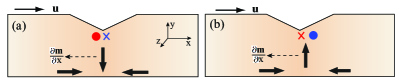
Empirically, we found that vortex/antivortex polarity is uniquely determined by the types of transverse wall and current direction. This result is based on more than twenty simulations that we have done by varying various parameters like notch geometry, wire width, magnetic anisotropy, damping etc. Within the picture that DW depinning starts from vortex/antivortex nucleation, the dependence of depinning current density can be understood as follows. For a clockwise (counterclockwise) transverse wall and current in direction, (), as shown in Fig. 6. If one assumes that vortex/antivortex formation starts from the vortex/antivortex core, it means that the core spin rotates into -direction for a vortex of . For a clockwise wall, -torque () tends to rotate core spin in -direction, as shown in Fig. 6a, so the presence of a small -torque tries to prevent the nucleation of vortices. Thus, the larger is, the higher will be. This may be the reason why the depinning current density increases as increases.
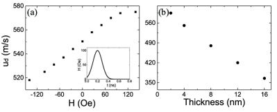
Our simulations suggest that DW depinning starts from vortex/antivortex nucleation. Adiabatic spin transfer torque tends to rotate the spins at the edge defect near a notch out of plane and to form a vortex/antivortex core. Thus, any mechanisms that help (hinder) the creation of a vortex/antivortex core shall decrease (increase) the depinning current density . To test this hypothesis, we use a magnetic field pulse of 0.4 ns along direction (shown in the inset of Fig. 7a) such that the field torque rotates spins out of plane. Figure 7a is the numerical results of the magnetic field dependence of the depinning current density for a 64 nm wide wire with triangular notches of 48 nm wide and 16 nm deep. The non-adiabatic coefficient is . As expected, decreases (increases) with field when it is along -direction (+direction) so that spins rotate into +direction (-direction). All other parameters are the same as those for Fig. 2.
If the picture is correct, one should also expect the depinning current density depends on the wire thickness. The shape anisotropy impedes vortex core formation because it does not favor a spin aligning in the direction. The shape anisotropy decreases as the thickness increases. Thus, one should expect the depinning current density decreases with the increase of wire thickness. Indeed, numerical results shown in Fig. 7b verifies the conjecture. All other parameters are the same as that in Fig. 7a ().
IV.2 Width effects on the depinning current density
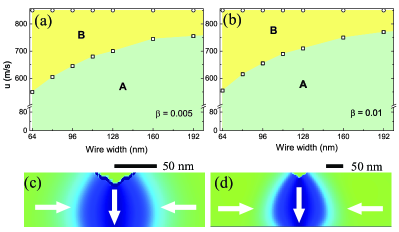
The DW propagating boost shown above is from the wire in which the notch depth (16 nm) is relatively big in comparison with wire width (64 nm). Naturally, one may ask whether the DW propagation boost exists also in a wire when the notch depth is much smaller than the wire width. To address the issue, we fix the notch geometry and vary the wire width. Figure 8 is the nanowire width dependence of depinning current density when the notch size is fixed at . Figures 8a and 8b show the phase boundary between vortex-assisted boosting phase and the pinning phase. DW propagation boost exists when nanowire width is one order of magnitude larger than the notch depth. The top view of the wire and spin configurations for 64 nm wide and 160 nm wide wires are shown in Fig. 8c and Fig. 8d, respectively.
IV.3 DW Propagation and vortex dynamics
DW propagation boost and slow-down by vortices can be understood from the Thiele equation [26, 27, 10],
| (1) |
where is the external force related to magnetic field that is zero in our case, is gyrovector that is zero for a transverse wall and for a 2D vortex wall, where is the winding number (+1 for a vortex and -1 for an antivortex), is vortex polarity ( for core spin in direction) and is the thickness of the nanowire. is dissipation dyadic, whose none zero elements for a vortex/antivortex wall are [27], where is nanowire width and is the Thiele DW width [26]. is the DW velocity.
For a transverse wall, (solid lines) agrees perfectly with numerical results (open symbols) in homogeneous wires as shown in Figs. 2b and 3b without any fitting parameters. For a vortex wall, the DW velocity is
| (2) |
| (3) |
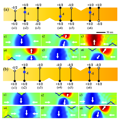
depends on DW width, as well as . For a given vortex wall, has opposite sign for and . In terms of topological classification of defects [23], the edge defect of the transverse DW at the first notch (Fig. 1a) has winding number , and this edge defect can only give birth to an antivortex of and while itself changes to an edge defect of as shown in Fig. 9a. Empirically, we found that antivortex polarity is uniquely determined by the types of transverse wall and current direction. A movie visualizing the DW propagation in boosting phase is shown in the Supplemental Movie [25]. All the parameters are the same as the inset of Fig. 2b. The three segments of identical length 1200 nm are connected in series to form a long wire. When , the antivortex moves downward () to the lower edge defect of winding number of . The lower edge defect changes its winding number to and the transverse DW reverses its chirality [24] when the vortex merges with the edge defect. Then another antivortex of winding number and is generated at the second notch on the lower wire edge and it moves upward (). The DW reverses its chirality again at upper wire edge when the antivortex dies. Then this cycle repeats itself. The spin configurations corresponding to various stages are shown in the lower panels of Fig. 9a. When , as shown in Fig. 9b, the antivortex of and moves upward since . The chirality of the original transverse wall shall not change when the antivortex is annihilated at the upper edge defect because of winding number conservation. No antivortex is generated at the even number notches and same type of the antivortex is generated at odd number notches, hence the transverse wall preserves its chirality throughout propagation. The corresponding spin configurations are shown in the lower panels of Fig. 9b.
The second term in Eq. (3) (for ) is , the same as the transverse DW velocity in a homogeneous wire (straight lines in Figs. 2b and 3b). The first term depends on DW properties as well as and . It changes sign at . is larger than in the presence of vortices if . Therefore, in this case vortex generations and vortex dynamics boost DW propagation. For small and to the leading order correction in and , Eq. (3) becomes . Thus, the longitudinal velocity equals approximately and depends very weakly on . This is what was observed in Fig. 2b. corresponds to the complete conversion of itinerant electron spins into local magnetic moments. Although the Thiele equation cannot explain why a DW generates vortices around notches in phase B, it explains well DW propagation boost for . This result is in contrast to the field-driven DW propagation where vortex/antivortex generation reduces the Walker breakdown field and inevitably slows down DW motion [5, 24].
Before conclusion, we would also like to point out that it is possible to realize both (boosting phase) and (hindering phase) experimentally in magnetic materials like permalloy with damping coefficient engineering. A recent study [28] demonstrated that of permalloy can increase by four times through a dilute impurity doping of lanthanides (Sm, Dy, and Ho).
V Conclusions
In conclusion, notches can boost DW propagation when . The boost is facilitated by antivortex generation and motion, and boosting effect is optimal when two neighboring notches is separated by the distance that an antivortex travels in its lifetime. In the boosting phase, DW can propagate at velocity that corresponds to a complete conversion of itinerant electron spins into local magnetic moments. When , the notches always hinder DW propagation. According to Thiele’s theory, the generation of vortices increases DW velocity for and decreases DW velocity when . This explains the origin of boosting phase and hindering phase. Furthermore, it is found that a vortex wall favored in a very wide wire tends to transform to a transverse wall under a current. This may explain experimental observation that the depinning current density is not sensitive to DW types.
VI acknowledgments
We thank Gerrit Bauer for useful comments. HYY acknowledges the support of Hong Kong PhD Fellowship. This work was supported by NSFC of China (11374249) as well as Hong Kong RGC Grants (163011151 and 605413).
References
- [1] S. S. P. Parkin, M. Hayashi, and L. Thomas, Science 320, 190 (2008).
- [2] D. A. Allwood, G. Xiong, C. C. Faulkner, D. Atkinson, D. Petit, and R. P. Cowburn, Science 309, 1688 (2005).
- [3] M. Kläui, C. A. F. Vaz, J. A. C. Bland, W. Wernsdorfer, G. Faini, E. Cambril, L. J. Heyderman, F. Nolting, and U. Rüdiger, Phys. Rev. Lett. 94, 106601 (2005).
- [4] M. Hayashi, L. Thomas, C. Rettner, R. Moriya, X. Jiang, and S. S. P. Parkin, Phys. Rev. Lett. 97, 207205 (2006).
- [5] Y. Nakatani, A. Thiaville, and J. Miltat, Nat. Mater. 2, 521 (2003).
- [6] X. R. Wang, P. Yan, J. Lu and C. He, Ann. Phys. (N.Y.) 324, 1815 (2009); X. R. Wang, P. Yan, and J. Lu, Europhys. Lett. 86, 67001 (2009).
- [7] L. Berger, J. Appl. Phys. 55, 1954 (1984).
- [8] J. C. Slonczewski, J. Magn. Magn. Mater. 159, L1 (1996).
- [9] S. Zhang and Z. Li, Phys. Rev. Lett. 93, 127204 (2004).
- [10] A. Thiaville, Y. Nakatani, J. Miltat, and Y. Suzuki, Europhys. Lett. 69, 990 (2005).
- [11] Z. Li and S. Zhang, Phys. Rev. B 70, 024417 (2004).
- [12] G. Tatara and H. Kohno, Phys. Rev. Lett. 92, 086601 (2004).
- [13] H. Y. Yuan and X. R. Wang, European Physical Journal B (in press); arXiv:1407.4559 [cond-mat.mes-hall]
- [14] R. D. McMichael and M. J. Donahue, IEEE Trans. Magn. 33, 4167 (1997).
- [15] G. S. D. Beach, C. Knutson, C. Nistor, M. Tsoi, and J. L. Erskine, Phys. Rev. Lett. 97, 057203 (2006).
- [16] L. Thomas, R. Moriya, C. Rettner, and S. S. P. Parkin, Science 330, 1810 (2010).
- [17] http://math.nist.gov/oommf.
- [18] A. Vansteenkiste, J. Leliaert, M. Dvornik, M. Helsen, F. Garcia-Sanchez, F. B. V. Waeyenberge, AIP Adbances 4, 107133 (2014).
- [19] OOMMF package was used in the early stage of this research. In order to simulate a long and wide wire, we switched to MUMAX package. Two packages give almost identical results on shorter wires, and the results presented here were generated from MUMAX.
- [20] B. Hu and X. R. Wang, Phys. Rev. Lett. 111, 027205 (2013); X. S. Wang, P. Yan, Y. H. Shen, G. E.W. Bauer, and X. R. Wang, Phys. Rev. Lett. 109, 167209 (2012).
- [21] Notch geometry affects depinning current because of the change of current density and perpendicular shape anisotropy (see Ref. 22) in notch area. Both effects help to generate vortices and thus reduce the depinning current. This may explain the result.
- [22] A. Aharoni, J. Appl. Phys. 83, 3432 (1998).
- [23] O. Tchernyshyov and G. -W. Chern, Phys. Rev. Lett. 95, 197204 (2005).
- [24] H. Y. Yuan and X. R. Wang, J. Magn. Magn. Mater. 368, 70 (2014).
- [25] See Supplemental Material at [URL] for DW propagation in boosting phase.
- [26] A. A. Thiele, Phys. Rev. Lett. 30, 230 (1973).
- [27] D. L. Huber, Phys. Rev. B 26, 3758 (1982).
- [28] S. G. Reidy, L. Cheng, and W. E. Bailey, Appl. Phys. Lett. 82, 1254 (2003).