Coherence times of precisely depth controlled NV centers in diamond
Abstract
We investigated the depth dependence of coherence times of nitrogen-vacancy (NV) centers through precisely depth controlling by a moderately oxidative at 580 ∘C in air. By successive nanoscale etching, NV centers could be brought close to the diamond surface step by step, which enable us to trace the evolution of the number of NV centers remained in the chip and to study the depth dependence of coherence times of NV centers with the diamond etching. Our results showed that the coherence times of NV centers declined rapidly with the depth reduction in their last about 22 nm before they finally disappeared, revealing a critical depth for the influence of rapid fluctuating surface spin bath. By monitoring the coherence time variation with depth, we could make a shallow NV center with long coherence time for detecting external spins with high sensitivity.
In recent years, shallow NV center has attracted increasing attention owing to its applications in nanoscale spin detectionkey-1 ; key-2 ; key-3 ; key-4 ; key-5 ; key-6 ; key-7 and surface spin noise investigationkey-8 ; key-9 ; key-10 ; key-11 . Since the minimum detectable magnetic dipole moment scales as key-9 ; key-12 ; key-13 , where r is the NV-target spin distance and is the coherence times of the NV center, the nanoscale control of the NV center depth and the investigation of depth dependence of NV center coherence time are important.
Recently, two methods, plasma etching key-14 and oxidative etching key-13 ; key-15 , have been developed to control the depth of the NV center. Cui et al. found that the conventional oxygen plasma etching had low damage to diamond key-14 . For oxidative etching, Kim et al. demonstrated that the diamond could be etched at the temperature, ranging from 550 ∘C to 620 ∘C, in pure oxygen gas key-13 . Loretz et al. reported that the oxidative etching rate for diamond was about 10 at 650 ∘C in air and by using this method they realized a 1.9-nm-deep NV center key-15 . However, the etching rate was not short enough to precisely control the depth of NV center .
In this work, we performed oxidative etching in air on diamond at a reduced oxidative temperature 580 ∘C, obtaining about 1.1 nm/h etching rate. By successive nanoscale etching, NV centers could be brought close to the diamond surface step by step, which enable us to investigate the depth dependence of coherence times of NV centers. The coherence time of NV center declined rapidly with the depth reduction in their last about 22 nm before they finally disappeared, which was attributed to the influence of the rapid fluctuating surface spin bath. By monitoring the coherence time variation with depth, we could make a shallow NV center with long coherence time for detecting external spins with high sensitivitykey-5 ; key-7 ; key-15 ; key-16 .
A mm3 (100) electronic grade diamond chip from Element Six ([]=1.1%, [N]<5 ppb) was used for the experiments. At first, a 300-nm-thick polymethyl methacrylate (PMMA) layer was deposited on the diamond chip surface key-17 ; key-18 . Then a series of 60 nm diameter apertures, as well as some 10- -wide strips used as position marks key-18 , were patterned on the PMMA layer using electron beam lithography. The NV centers in the chip were generated by implanting 60 keV molecules with a fluence through the apertures and strips on the PMMA layer.key-17 ; key-18 . After implantation, the sample was annealed at 1050 ∘C in a vacuum at Pa for 2 h to form long spin coherence time NV centers key-19 . After oxidation at 430 ∘C in air for 2.5 h, the sample was cleaned in a 1:1:1 boiling mixture of sulfuric, nitric, and perchloric acid at 200 ∘C for 2 hours.
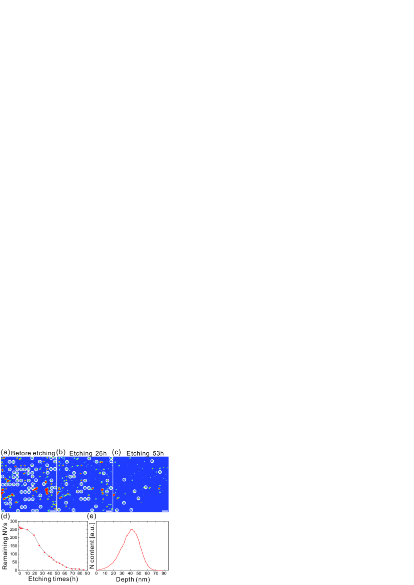
The oxidative etching was performed in air on the diamond chip situated in a box furnace with its implanted side up. In order to have a slow etching rate, we used a lower oxidative temperature of 580 ∘C. The diamond chip was put in the furnace when the furnace temperature had already stabilized at 580 ∘C. The process for the furnace temperature being stabilized at 580 ∘C only took about 1 minute. Similarly, when the etching process was finished, we directly took the diamond chip out to the air for cool down. We traced the evolution of the number of single NV centers remaining in the chip with the etching time and investigated the relationship between the coherence times of the NV centers and the etching times. Figure 1(a) showed the fluorescence image of a representative area of the diamond chip before oxidative etching, with the traced single NV centers marked with circles in the figure. The larger bright specks in the image were NV center clusters produced in the implantation due to imperfection of the PMMA templet layer deposited on the diamond chip key-18 . After oxidative etching for 26 h, the image of the same area showed less single NV centers and the bright specks of the NV center clusters also became less bright and smaller [Fig. 1(b)]. As shown in Fig. 1(c), after oxidative etching for 53 h, there were only few single NV centers remained on the chip and the bright specks became even less bright and smaller. These results clearly demonstrated that the NV centers originally situated at different depths of the diamond chip had been removed successively by oxidative etching key-13 ; key-15 .
We traced 265 single NV centers that were initially in the diamond chip. As shown in Fig. 1(d), the number of the remaining single NV centers in the chip reduced with the oxidative etching times. We found that when the etching time was less than 10 h, the number of the remaining NV centers reduced very little. Then, when the etching times increased from 10 h to about 60 h, the NV centers number reduced rapidly. After that, the number reduced slowly and finally almost all the NV centers finally disappeared after 85 h etching. The results showed that the number of the remaining single NV centers reduced about 70% after etching 42 h. By comparing the above results with the SRIM simulations for an implantation nitrogen atom energy of 30 keV [Fig. 1(e)], we found that the etching depth corresponding to 42 h etching was 46 nm. Therefore, we estimated that the etching rate was about 1.1 nm/h at 580 C in air.
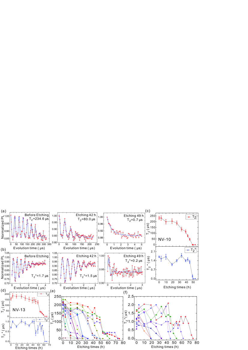
The slow etching rate made it possible to control the depth of the NV center at nanoscale. Thus, we could precisely trace the evolution of the coherence time of a single NV center with its depth, which reflected the variation in its local environment, from the bulk spin bath to the surface spin bath. A set of randomly selected 20 single NV centers [named NV-1 through 20] with their axes parallel to the external magnetic field (47 G) was used for the tracing. We performed spin echo measurements for all the 20 single NV centers before the chip etching, and found that the of 19 NV centers among them were between 134 and 234 , and the other one was 3.3 . The mean value of of the 19 single NV centers was about 194 , which was comparable to that of the native NV center inside electronic grade diamond key-20 , implying that the NVs were initially deep inside the chip and the initial major spin impurities were .
Then, we measured the coherence times of the 20 NV centers after successively etching for various times step by step. Fig. 2(a) showed three representative results of the spin echo measurements for NV-10 (which just disappeared after etching 50 h), after different oxidative etching times. In the first two figures, we found that the photoluminescence (PL) profile collapsed and revived at Larmor frequency (about 50.3 kHz), which was due to the incoherent precession of the 13C nuclei spins in our natural abundance sampleskey-21 . It was found that for the sample before etching, the of NV-10 was 234.6 . And, after an etching of 42 h, the declined to 80 . However, when the etching time reached 49 h, its PL intensity was not stable and was reduced to about half of the initial value, indicating that the center had been very shallow and its charge state had become unstable key-22 ; key-23 . (The similar phenomenon was also observed for other NV centers, when they were shallow enough by long time etching.) Moreover, its was reduced to only about 0.7 . The above results revealed that the NV center became very shallow and suffered a strong influence of the rapid fluctuating surface spin bath key-8 ; key-9 ; key-10 ; key-24 . The of NV-10 in the sample etched for various times were presented in Fig. 2(c) top. This etching time dependence can be converted to the depth dependence as the depth varied with the etching time. As shown from the figure, for short etching time (less than about 30 h), the decreased slowly with the etching time, then declined rapidly in its last about 20 h etching before it finally disappeared (i.e. when its depth was less than about 22 nm). Finally, when the etching time was longer than 50 h, NV-10 was finally disappeared.
Three representative Ramsey measurements for NV-10 were also shown in Fig. 2(b), and its for the sample after various etching times were summarized in Fig. 2(c) bottom. We could see that the had a similar evolution to the . As another example, Figure 2(d) gave the results of the coherence time measurements for NV-13 (just disappeared after etching 62 h). It is clear that the coherence time decreased very slowly with the etching time in the initial 40 h, while declined rapidly in the last 20 h etching before it finally disappeared (i.e. when its depth was less than about 22 nm). The evolution were similar to that of NV-10. Fig. 2(e) summarized the dependences of with the etching time for all the 20 NV centers. We found that there was a similar dependence for all these NV centers: the of each NV centers decreased rapidly when the etching time was about 20 h before the centers finally disappeared (i.e. when their depth became less than about 22 nm). The results of Ramsey measurements of the 9 representative single NV centers after different oxidative etching times were shown in Fig. 2(f), which exhibited a similar variation as that of their in Fig. 2(e). The results suggested that, when the depth decreased to about 22 nm, rapidly fluctuating surface spins, compared with the slow bulk spin bath, began to play an important role in NV decoherence, leading to a rapid decreasing in coherence time with a further decrease in centers depth, which was consistent with the results of the delta doping NV centers key-9 .
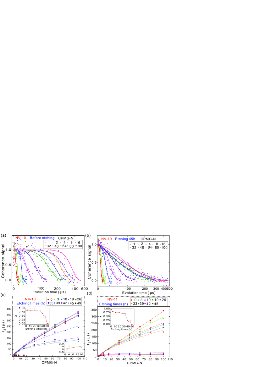
Dynamical decoupling was important in NV center based high sensitivity magnetic field key-25 and temperature key-18 ; key-26 sensing. In particular, the shallow NV centers, combined with dynamical decoupling, could also be used to detect external spins key-3 ; key-5 ; key-6 ; key-7 and investigate the surface spin noise key-9 ; key-10 ; key-11 . In view of this, we performed CPMG measurements on three arbitrarily selected NV centers (NV-1, 10, 11) on the chip after different oxidative etching times. The results were shown in Fig. 3. As shown in Fig. 3(a), before etching, the of the CPMG-N of NV-10 were always increasing with the pulse number N, in particular, the of the CPMG-100 was about 360.4 , about 52 times longer than the value 6.9 for the spin echo. However, in Fig. 3(b), after etching for 45 h, almost all the of the CPMG-N were declined, in particular, the of the CPMG-100 was about 120.4 , which was only about one third of the value before etching. The of the CPMG-N as a function of N for NV-10 with the chip etched for various times were summarized in Fig. 3(c). The decoupling efficiencies key-9 varied with the etching time were shown in the inset (top left) of Fig. 3(c). When the etching time was less than about 30 h, the of the CPMG were decreased very slowly, and the decoupling efficiencies was nearly a constant of about 0.82. This was consistent to the fact that the center, for sample etched for 30 h, was still inside the chip and the main spin bath was a bulk bathkey-20 . Then, they both declined rapidly when its depth decreasing in its last about 20 h etching before it finally disappeared (i.e. when its depth was less than about 22 nm), which was similar to the results in Fig. 2(c). The similar phenomena were observed for NV-11 (just disappeared after etching 48 h) [Fig. 3(d)] and NV-1 (just disappeared after etching 75 h, and its data was not shown in this paper). The results were consistent with the fact that when the depth of the NV centers decreased, they would have a higher coupling strength with surface spin bath that had a fast fluctuation rate key-9 ; key-10 .
In summary, we investigated the depth dependence of coherence times of NV centers in diamond with the depth controlled using oxidative etching. We used a lower oxidative temperature of 580 ∘C in air to reduce the etching rate to about 1.1 nm/h. Thus, we can more precisely control the depth of the centers. On the basis of this, we performed the spin echo and Ramsey and CPMG measurements on the NV centers, of which the depth was decreased by successive oxidative etching, and found that the coherence times of NV centers declined rapidly with the depth reduction in their last about 22 nm etching before they finally disappeared, revealing a critical depth for the influence of rapid fluctuating surface spin bath, which was consistent with the results of the delta doping NV centers. key-9 . The obtained results showed how the surface spin influenced the coherence behavior of NV centers of different depths, paving the way for investigating surface spins. Particularly, the slow etching method make it possible to control the depth of the NV center at nanoscale, which can be used to study the stability of the very shallow NV centers key-24 ; key-25 ; key-27 , to investigate the surface spin noise key-8 ; key-9 ; key-10 ; key-11 , and for high sensitivity (even for single electron and nuclear) nanoscale spin detection key-5 ; key-7 ; key-15 ; key-16 . Moreover, it can also be used to control the depth of the NV center in the diamond tip equipped to the atomic force microscope, which can be used in high sensitivity nanoscale magnetic imaging of the spins key-28 .
This work was supported by the National Basic Research Program of China (2013CB921800, 2011CB921400) and the Natural Science Foundation of China (Grants No. 11374280 and No. 50772110).
References
- (1) B. Grotz, J. Beck, P. Neumann, B. Naydenov, R. Reuter, F. Reinhard, F. Jelezko, J. Wrachtrup, D. Schweinfurth, B. Sarkar, and P. Hemmer, New J. Phys. 13, 055004 (2011).
- (2) H. J. Mamin, M. H. Sherwood, and D. Rugar, Phys. Rev. B 86, 195422 (2012).
- (3) T. Staudacher, F. Shi, S. Pezzagna, J. Meijer, J. Du, C. A. Meriles, F. Reinhard, and J. Wrachtrup, Science 339, 561 (2013).
- (4) H. J. Mamin, M. Kim, M. H. Sherwood, C. T. Rettner, K. Ohno, D. D. Awschalom, and D. Rugar, Science 339, 557 (2013).
- (5) C. Müller, X. Kong, J.-M. Cai, K. Melentijević, A. Stacey, M. Markham, D. Twitchen, J. Isoya, S. Pezzagna, J. Meijer, J. F. Du, M. B. Plenio, B. Naydenov, L. P. McGuinness, and F. Jelezko, Nat. Commun. 5, 4703 (2014).
- (6) S. J. DeVience, L. M. Pham, I. Lovchinsky, A. O. Sushkov, N. Bar-Gill, C. Belthangady, F. Casola, M. Corbett, H. Zhang, M. Lukin, H.K. Park, A.Yacoby, and R. L. Walsworth, Nat. Nano. 10, 129 (2015).
- (7) F. Z. Shi, Q. Zhang, P. F. Wang, H. B. Sun, J. R. Wang, X. Rong, M. Chen, C. Y. Ju, F. Reinhard, H. W. Chen, J. Wrachtrup, J. F. Wang, and J. F. Du, Science 347, 1135 (2015).
- (8) T. Rosskopf, A. Dussaux, K. Ohashi, M. Loretz, R. Schirhagl, H. Watanabe, S. Shikata, K. M. Itoh, and C. L. Degen, Phys. Rev. Lett. 112, 147602 (2014).
- (9) B. A. Myers, M. C. Dartiailh, K. Ohno, A. Das, D. D. Awschalom, and A. C. B. Jayich, Phys. Rev. Lett. 113, 027602 (2014).
- (10) Y. Romach, C. Muller, T. Unden, L. J. Rogers, T. Isoda, K. M. Itoh, M. Markham, A. Stacey, J. Meijer, S. Pezzagna, B. Naydenov, L. P. McGuinness, N. Bar-Gill, and F. Jelezko, Phys. Rev. Lett. 114, 017601 (2015).
- (11) L. Luan, M. S. Grinolds, S.K. Hong, P. Maletinsky, R. L. Walsworth, and A. Yacoby, Sci. Rep. 5, 8119 (2015).
- (12) J. R. Maze, P. L. Stanwix, J. S. Hodges, S. Hong, J. M. Taylor, P. Cappellaro, L. Jiang, M. V. Gurudev Dutt, E. Togan, A. S. Zibrov, A. Yacoby, R. L. Walsworth, and M. D. Lukin, Nature (London) 455, 644 (2008).
- (13) M. Kim, H. J. Mamin, M. H. Sherwood, C. T. Rettner, J. Frommer, and D. Rugar, Appl. Phys. Lett. 105, 042406 (2014).
- (14) S. Y. Cui, A. S. Greenspon, K. Ohno, B. A. Myers, A. C. Bleszynski Jayich, D. D. Awschalom, and E. L. Hu, Nano Lett. 15, 2887 (2015).
- (15) M. Loretz, S. Pezzagna, J. Meijer, and C. L. Degen, Appl. Phys. Lett. 104, 033102 (2014).
- (16) A. O. Sushkov, I. Lovchinsky, N. Chisholm, R. L. Walsworth, H. Park, and M. D. Lukin, Phys. Rev. Lett. 113, 197601 (2014).
- (17) P. Spinicelli, A. Dréau, L. Rondin, F. Silva, J. Achard, S. Xavier, S. Bansropun, T. Debuisschert, S. Pezzagna, J. Meijer, V. Jacques, and J.-F. Roch, New J. Phys. 13, 025014 (2011).
- (18) J. F. Wang, F. P. Feng, J. Zhang, J. H. Chen, Z. C. Zheng, L. P. Guo, W. L. Zhang, X. R. Song, G. P. Guo, L. L. Fan, C.W. Zou, L. R. Lou, W. Zhu, and G. Z Wang, Phys. Rev. B 91, 155404 (2015)
- (19) T. Yamamoto, T. Umeda, K. Watanabe, S. Onoda, M. L. Markham, D. J. Twitchen, B. Naydenov, L. P. McGuinness, T. Teraji, S. Koizumi, F. Dolde, H. Fedder, J. Honert, J. Wrachtrup, T. Ohshima, F. Jelezko, and J. Isoya, Phys. Rev. B 88, 075206 (2013).
- (20) C. A. Ryan, J. S. Hodges, and D. G. Cory, Phys. Rev. Lett. 105, 200402 (2010).
- (21) L. Childress, M. V. Gurudev Dutt, J. M. Taylor, A. S. Zibrov, F. Jelezko, J. Wrachtrup, P. R. Hemmer, and M. D. Lukin, Science 314, 281 (2006).
- (22) R. Schirhagl, K. Chang, M. Loretz, and C. L. Degen, Annu. Rev. Phys. Chem. 65, 83 (2014).
- (23) C. Bradac, T. Gaebel, N. Naidoo, M. J. Sellars, J. Twamley, L. J. Brown, A. S. Barnard, T. Plakhotnik, A. V. Zvyagin, and J. R. Rabeau, Nat. Nanotechnol. 5, 345 (2010).
- (24) B. K. Ofori-Okai, S. Pezzagna, K. Chang, M. Loretz, R. Schirhagl, Y. Tao, B. A. Moores, K. Groot-Berning, J. Meijer, and C. L. Degen, Phys. Rev. B 86, 081406 (R) (2012).
- (25) L. M. Pham, N. Bar-Gill, C. Belthangady, D. Le Sage, P. Cappellaro, M. D. Lukin, A. Yacoby, and R. L. Walsworth, Phys. Rev. B 86, 045214 (2012).
- (26) D. M. Toyli, C. F. de las Casas, D. J. Christle, V. V. Dobrovitski, and D. D. Awschalom, Proc. Natl. Acad. Sci. USA 110, 8417 (2013).
- (27) I. I. Vlasov, A. A. Shiryaev, T. Rendler, S. Steinert, S.-Y. Lee, D. Antonov, M. Vörös, F. Jelezko, A. V. Fisenko, L. F. Semjonova et al., Nat. Nanotechnol. 9, 54 (2013).
- (28) M. S. Grinolds, S. Hong, P. Maletinsky, L. Luan, M. D. Lukin, R. L. Walsworth, and A. Yacoby, Nat. Phys. 9, 215 (2014).