Strain induced topological phase transitions in monolayer honeycomb structures of group-V binary compounds
Abstract
We present first-principles calculations of electronic structures of a class of two-dimensional (2D) honeycomb structures of group-V binary compounds. Our results show these new 2D materials are stable semiconductors with direct or indirect band gaps. The band gap can be tuned by applying lattice strain. During their stretchable regime, they all exhibit metal-indirect gap semiconductor-direct gap semiconductor-topological insulator (TI) transitions with increasing strain from negative (compressive) to positive (tensile) values. The topological phase transition results from the band inversion at point due to lattice strain and is irrelevant to spin-orbit coupling (SOC).
keywords:
Electronic structures, 2D Topological insulators, Topological phase transition, First-principles calculations, Strain engineering![[Uncaptioned image]](/html/1507.06068/assets/x1.png)
Two-dimensional (2D) topological insulators (TIs), also known as quantum spin Hall (QSH) insulators, have attracted much attention recent years due to their rich physics and promising applications in spintronics and quantum computations1, 2, 3, 4. The QSH effect, which was first proposed in graphene5, describes the existence of the edge states on the sides of a 2D TI system. These edge states are supposed to consist of two counter-propagating oppositely spin polarized edge channels in the band gap of the material. However, the spin-orbit coupling (SOC) in graphene is too weak to open a gap large enough to support accessible QSH effect experimentally. Unlike graphene, its elemental analogues - silicene and germanene, show energy gaps because they have larger SOC due to their buckled honeycomb structures6. Therefore, QSH effect can be observed in an experimentally accessible temperature regime in both systems7. Other monolayer honeycomb structures of group-IV elements as well as III-V binary compounds have been systematically investigated based on first-principles calculations8. Theoretical studies show that many of these materials are 2D TIs at the equilibrium structure, including stanene9, InBi, GaBi, and TlBi10, 11. Most recently, there has been rising interest in layered compounds of group-V elements12, 13, 14, 15, 16. Elemental phosphorus have a large number of allotypes. Among them, blue phosphorous has the same layered structure as bulk arsenic, antimony, and bismuth. Their corresponding monolayer materials have the same buckled honeycomb structure as silicene and germanene12, 17. Monolayer bismuth is reported a 2D TI, while other monolayer buckled honeycomb structures of group-V elements are conventional semiconductors18, 19, 20. Furthermore, recent studies indicate that band topology in these 2D materials could be altered by chemical adsorptions21, 22, 23, external electric field24, 25, and lattice strain25, 26, 27. Under lattice strain, monolayer honeycomb structure of P, As, and Sb all exhibit trivial semiconductor to TI transition27. However, the mechanism of the topological phase transition under lattice strain has not been revealed. We also note that there is no report of monolayer honeycomb structures of group-V binary compounds, although bulk AsSb has the same layered structure as bulk arsenic, antimony, and bismuth28.
In this paper, we study monolayer honeycomb structures of group-V binary compounds (except nitrogen) by first-principles calculations. We investigate the stability of these new 2D materials by studying phonon dispersion and molecular dynamical simulations, and calculate their band structures under lattice strains. We find all of them are stable semiconductors with indirect or direct energy gaps. Under strain, they all exhibit metal-indirect gap semiconductor-direct gap semiconductor-topological insulator (TI) transitions. It is noteworthy that the mechanism of topological transition is due to the different response of energies of the valence band and the conduct band at point under lattice strain, and is irrelevant to SOC, which is previously supposed to be indispensable for realizing TIs.
Our first-principles calculations are carried out in the framework of density-functional theory (DFT)29 within the Perdew-Burke-Ernzerhof generalized gradient approximation (GGA)30 implemented in the ABINIT codes31. Norm-conserving HGH pseudopotentials32 and the plane-wave cutoff energy of 30 Hartree are used. For monolayer binary compounds, a supercell with a vacuum space of 20 Å along the z-direction is employed with a k-point mesh. Both the lattice parameters and the positions of all atoms are relaxed until the force is less than 1 meV/Å. The phonon frequencies are computed using density-functional perturbation theory (DFPT)33 with a q-point mesh. We perform canonical molecular dynamics (MD) simulation at 300K with a supercell of 72 atoms. The length of time-step of 3 fs and simulations with 500 steps are executed.
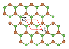
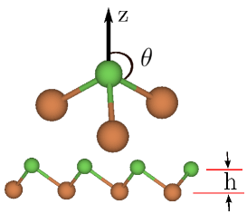
Bulk AsSb, or arsenic antimonide, has the same layered crystal structure as arsenic, antimony, and bismuth (space group Rm, No.166), with the intermediate values of lattice parameters of arsenic and antimony, Å, Å. Like monolayer As and Sb, we consider monolayer AsSb consisting of a layer of As and a layer of Sb. This new material has the same structure as silicene and germinene, i.e. the buckled honeycomb structure, as shown in Figure 1. We perform geometry optimization for such a monolayer AsSb, obtain the lattice constants Å, and calculate the binding energy. Motivated by this, we consider all possible group-V binary compounds (except nitrogen) with the same structure. The optimized lattice constants, buckled parameters, and binding energies are calculated, and the corresponding parameters of monolayer P, As ,Sb, and Bi are also given for the sake of comparison (see Supporting Information for more detail).
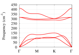
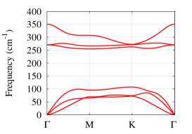
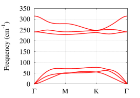
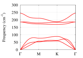
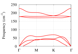
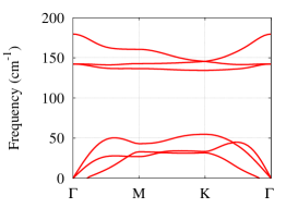
To check the stability, we calculate the phonon dispersion of these monolayer binary compounds. Absence of negative frequencies of the calculated phonon dispersion indicates the stability of monolayer PAs, PSb, PBi, and AsSb (see Figure 2). Note that although ZA branch (out of plane acoustical modes) becomes soft and get imaginary frequencies near point for AsBi and SbBi, it is believed such instability can be removed by the defects6, 8. On the other hand, the ZA imaginary frequencies around point also depends on the mesh size used in the calculations. It may be an artifact of the mesh size6, 8. The MD simulations also show the stability of these 2D compounds because no structural collapse happens during the simulations (see Supporting Information for more detail).
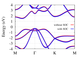
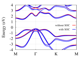
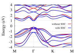
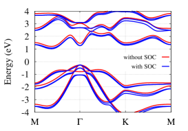
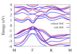
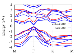
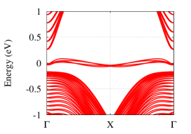
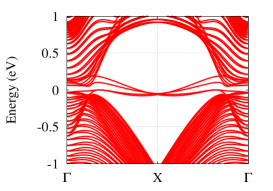
Figure 3 shows band structures of these binary compounds. The band structures of monolayer phosphorous, arsenic, antimony, and bismuth are also given for comparison (see Supporting Information for more detail). The calculated band structures (without SOC) show similarities between different systems. This is not surprising, since these elements are chemically similar. Taking into account SOC, the number of bands of binary compounds is doubled due to the nonsymmetric structure and SOC. Note that SOC just modifies the band gaps but does not change band orders for these binary compounds, P, As, and Sb. However, the band structure of Bi differs from others when SOC is included. The parity of the states that form the valence and conduction bands is reversed at point. This exchange of bands is the consequence of the increased SOC in Bi, and Bi is reported a 2D topological insulator18. On the contrary, other 2D group-V elemental materials and binary compounds with the same buckled honeycomb structure are conventional insulators. Take monolayer AsSb for example, the calculated band structure (without SOC) shows it is a semiconductor with a indirect gap of 1.48 eV, while a gap of 1.73 eV at . The valence band maximum (VBM) is at point, and the conduct band minimum (CBM) is at point. The band structures (without SOC) of binary compounds containing Bi possess direct gaps, while others show indirect gaps.
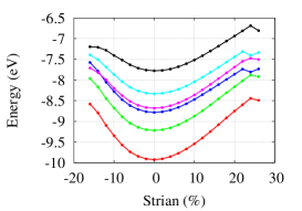
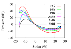
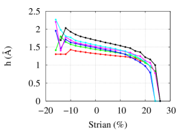
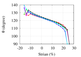
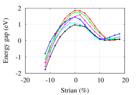
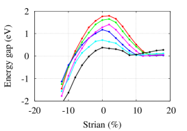
We perform strain engineering to these 2D binary compounds. Figure 4 shows calculated energies, pressures, buckling parameters, and energy gaps as functions of the strain. From the place where the stress maximum(minimum) occur we can determine the stretchability of the material. Take AsSb for example, the stretchability is about for press, and for stretch. During these domain, buckling parameters h and change almost linearly. When strain is larger than , h drops to zero and equals , and corresponding energy also changes rapidly. It means the system becomes planar honeycomb structure as graphene. Band gaps shown in Figure 4 (without SOC) and Figure 4 (with SOC) indicate that the system is metallic when strain is between and ; when strain is between and , the system is a indirect insulator; the system becomes a direct semiconductor with a gap at when strain is larger than . The band gap decreases with increasing strain and closes at about strain, then reopen when strain is larger than . Band structures of other binary compounds as well as P, As, and Sb under strain have similar characteristics (see Supporting Information for more detail).
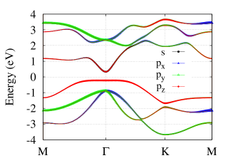
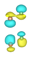
To get a better understanding of the mechanism underlying the band inversion, we investigate the band structure evolution at point. Take AsSb for example, As and Sb have five electrons in the outer shell. For each atom, two electrons occupy s orbital and three electrons occupy p orbitals. They form five energy bands below the Fermi energy. The two s bands are much lower than the three p bands. The three p bands of two atoms in the cell form six bands with three below the Fermi energy and three above the Fermi energy. According to our first-principles calculations, ignoring normalization factors, these six bands around point are mainly denoted by , (in fact, there are some and components in ), , , , and . A denotes As atom and B Sb atom. The , , and are below the Fermi energy while , , and are above the Fermi energy. When SOC is not included, and are degenerated, and so are and .
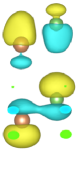
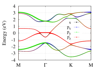
Under ambient conditions, is below and . When strain reaches up to , the indirect gap becomes a direct gap. When strain is , , , and have the same energy. When strain is beyond , the two bands below and above the Fermi energy at point is constructed by and , respectively. Figure 5 shows the band structures of monolayer AsSb at strain of and respectively, and the band composition. We see the band inversion at according to Figure 5(a) and Figure 5(c). Because h is relatively large when strain is small, the low half of is close to the upper half of , their coupling is bonding when they are out of phase, while their coupling is anti-bonding when they are in phase. Therefore has a lower energy than . Figure 5(b) shows and , corresponding to VBM and CBM, respectively. In other words, is the highest occupied molecular orbital (HOMO) at point, while is the lowest unoccupied molecular orbital (LUMO) at point. Note that shows and components. With further increase of strain, h decreases and the low half of is move from upper half of to low half of , then energy of increases and decrease. When strain is about , and have the same energy and the gap closes. When strain is larger than , the low half of is closer to the low half of because of small h, then their coupling is bonding when they are in phase, while their coupling is anti-bonding when they are out of phase, therefore has a higher energy than . Now is HOMO at point, while is LUMO at point, and the band inverts, as shown in Figure 5(c) and Figure 5(d).
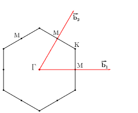
When A and B are the same element such as P, As, and Sb monolayer, the system has inversion symmetry. and orbitals have even and odd parity, respectively. The invariant can be determined from the parities of the occupied states at the time-reversal invariant momenta in the Brillouin zone34. There are four time-reversal invariant momenta for buckled honeycomb structure, i.e., one and three M points, as shown in Figure 1. The band inverts at means topological invariants changes. Directly parity counting at time reversal invariant momenta shows that the changes from 0 to 1 for monolayer P, As, and Sb, when stain is larger than (see Supporting Information for more detail). We note that As and Sb are reported to exhibit topological phase transition at tensile strain 27. However, this critical value is estimated according to bulk As and Sb lattice constants , which is about longer than that of corresponding 2D lattice constants26. Taking monolayer As and Sb lattice constants as bases, the critical value should be .
When A and B are different elements, the inversion symmetry is broken. Then , , and other states, are not the eigenstates of parity. Then it is not possible to determine the invariant from the symmetry of the occupied states at time-reversal invariant momenta. To check the topological invariants, we adopt the method proposed by Soluyanov and Vanderbilt35. The method is to track the largest gap between Wannier charge centers (WCCs). The path following the largest gap between WCCs cross the WCCs bands a number of times that is equal, mod 2, to the invariant. The calculated indices show AsSb is a conventional insulator under strain and a topological insulator under (see Supporting Information for more detail).
The mechanism of the band inversion at point is the different response of energies of and to lattice strain. The origin of the nontrivial topology in buckled honeycomb structures of group-V binary compounds (as well as monolayer P, As, and Sb with the same structure) results from the band inversion due to lattice strain. It is neither like the band inversion at point in monolayer Bi, HgTe quantum well, and , which is due to SOC, nor like that in silicene and germanene, which results from massive Dirac cone and there is no band inversion. In the case of these 2D honeycomb structures of group-V binary compounds, SOC just modifies energy gaps, as shown in Figure 4 and Figure 4. For example, monolayer AsSb, PBi, and SbBi exhibit topological energy gaps of 77, 333, and 69 meV under lattice strain without including SOC, respectively. Taking into account SOC, the corresponding energy gaps are 50, 29, and 247 meV, respectively.
Note that the existence of and components in does not change the mechanism of the band inversion mentioned above. However, it makes the difference between band dispersions of and near point. A remarkable feature can be seen that the band shows more flatter with increasing strain, in particular when it gets close to the Fermi energy. In fact, the band around point can be approximately given by (see Supporting Information for more detail)
| (1) |
When the energy of equals to that of , we have . It means the valency band becomes flat. On the contrary, the existence of and components in makes its band dispersive. In recent years, lattice models with flat bands have attracted attention for a number of reasons, among them are enhanced interaction effects36.
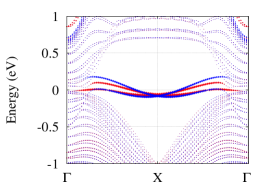
The existence of topological protected gapless edge states is one of the most important consequences of 2D topological insulators. To verify the edge states, we construct zigzag ribbons with 48 atoms in a unit cell (about 84.40 Å and 90.65 Å wide), under strain and , respectively. Figure 6 shows the calculated band structures. We observe both ribbons show band gaps, and inside the gap, as expected, we observe four states, corresponding to two spin-splitting edge states from either side of the ribbon inside bulk gap. AsSb ribbon has topologically protected gapless edge states under . Although gapless edge states are also shown under , they are not topologically protected.
In conclusion, we predict that monolayer honeycomb structures of group-V binary compounds are stable according to phonon dispersion and molecular dynamical simulations. These new 2D materials are semiconductors under ambient conditions. Monolayer PBi, AsBi, and SbBi possess direct gaps, while PAs, PSB, and AsSb possess indirect gaps. Under lattice strain, they show topological phase transitions according to calculated invariants. By constructing ribbons, we show topologically protected edge states exist at nontrivial topology phase. Analysis of the band structure evolution at point indicates that the band inversion is due to lattice strain and irrelevant to SOC. This mechanism of topological transition under lattice strain is different from that of previously studied 2D TIs, in which SOC is indispensable for nontrivial band topology. Therefore it is possible to seek nontrivial band topology in materials composed of constituents with lighter atoms and thus smaller SOC. We hope that our work will promote the research aiming at the synthesis of these new 2D materials and the search for new 2D TIs.
We wish to acknowledge the support of the National Natural Science Foundation No.11374373, Doctoral Fund of Ministry of Education of China (No.20120162110020), and the Natural Science Foundation of Hunan Province of China (No.13JJ2004).
References
- Hasan and Kane 2010 M. Z. Hasan and C. L. Kane, Reviews of Modern Physics 82, 3045 (2010), ISSN 0034-6861, 1539-0756, URL http://arxiv.org/abs/1002.3895.
- Moore and Balents 2007 J. E. Moore and L. Balents, Physical Review B 75, 121306 (2007), URL http://link.aps.org/doi/10.1103/PhysRevB.75.121306.
- Bernevig et al. 2006 B. A. Bernevig, T. L. Hughes, and S.-C. Zhang, Science 314, 1757 (2006), ISSN 0036-8075, 1095-9203, URL http://www.sciencemag.org/content/314/5806/1757.
- Qi and Zhang 2011 X.-L. Qi and S.-C. Zhang, Reviews of Modern Physics 83, 1057 (2011), URL http://link.aps.org/doi/10.1103/RevModPhys.83.1057.
- Kane and Mele 2005 C. L. Kane and E. J. Mele, Physical Review Letters 95, 146802 (2005), URL http://link.aps.org/doi/10.1103/PhysRevLett.95.146802.
- Cahangirov et al. 2009 S. Cahangirov, M. Topsakal, E. Aktürk, H. Şahin, and S. Ciraci, Physical Review Letters 102, 236804 (2009), URL http://link.aps.org/doi/10.1103/PhysRevLett.102.236804.
- Liu et al. 2006 B. Liu, Z. Qi, and C. Shi, Physical Review B (Condensed Matter and Materials Physics) 74, 174101 (pages 8) (2006), URL http://link.aps.org/abstract/PRB/v74/e174101.
- Şahin et al. 2009 H. Şahin, S. Cahangirov, M. Topsakal, E. Bekaroglu, E. Akturk, R. T. Senger, and S. Ciraci, Physical Review B 80, 155453 (2009), URL http://link.aps.org/doi/10.1103/PhysRevB.80.155453.
- Liu et al. 2011a C.-C. Liu, H. Jiang, and Y. Yao, Physical Review B 84, 195430 (2011a), URL http://link.aps.org/doi/10.1103/PhysRevB.84.195430.
- Chuang et al. 2014 F.-C. Chuang, L.-Z. Yao, Z.-Q. Huang, Y.-T. Liu, C.-H. Hsu, T. Das, H. Lin, and A. Bansil, Nano Letters 14, 2505 (2014), ISSN 1530-6984, URL http://dx.doi.org/10.1021/nl500206u.
- Huang et al. 2014a H. Huang, J. Liu, and W. Duan, Physical Review B 90, 195105 (2014a), URL http://link.aps.org/doi/10.1103/PhysRevB.90.195105.
- Guan et al. 2014 J. Guan, Z. Zhu, and D. Tománek, Physical Review Letters 113, 046804 (2014), URL http://link.aps.org/doi/10.1103/PhysRevLett.113.046804.
- Zhu and Tománek 2014 Z. Zhu and D. Tománek, Physical Review Letters 112, 176802 (2014), URL http://link.aps.org/doi/10.1103/PhysRevLett.112.176802.
- Peng et al. 2014 X. Peng, Q. Wei, and A. Copple, Physical Review B 90, 085402 (2014), URL http://link.aps.org/doi/10.1103/PhysRevB.90.085402.
- Fei and Yang 2014 R. Fei and L. Yang, arXiv:1403.1003 [cond-mat] (2014), URL http://arxiv.org/abs/1403.1003.
- Lee et al. 2014 J. Lee, W.-C. Tian, W.-L. Wang, and D.-X. Yao (2014), URL http://search.arxiv.org:8081/paper.jsp?r=1403.7858&qid=1431438623713mix_nCnN_1941975572qs=monolayer+arsenic+antimonyin=physics.
- Kamal and Ezawa 2015 C. Kamal and M. Ezawa, Physical Review B 91, 085423 (2015), URL http://link.aps.org/doi/10.1103/PhysRevB.91.085423.
- Liu et al. 2011b Z. Liu, C.-X. Liu, Y.-S. Wu, W.-H. Duan, F. Liu, and J. Wu, Physical Review Letters 107, 136805 (2011b), URL http://link.aps.org/doi/10.1103/PhysRevLett.107.136805.
- Yao et al. 2013 G. Yao, Z. Luo, F. Pan, W. Xu, Y. P. Feng, and X.-s. Wang, Scientific Reports 3 (2013), URL http://www.nature.com/srep/2013/130618/srep02010/full/srep02010.html.
- Wada et al. 2011 M. Wada, S. Murakami, F. Freimuth, and G. Bihlmayer, Physical Review B 83, 121310 (2011), URL http://link.aps.org/doi/10.1103/PhysRevB.83.121310.
- Song et al. 2014 Z. Song, C.-C. Liu, J. Yang, J. Han, M. Ye, B. Fu, Y. Yang, Q. Niu, J. Lu, and Y. Yao, NPG Asia Materials 6, e147 (2014), URL http://www.nature.com/am/journal/v6/n12/full/am2014113a.html.
- Ma et al. 2015 Y. Ma, Y. Dai, L. Kou, T. Frauenheim, and T. Heine, Nano Letters 15, 1083 (2015), ISSN 1530-6984, URL http://dx.doi.org/10.1021/nl504037u.
- Jin and Jhi 2015 K.-H. Jin and S.-H. Jhi, Scientific Reports 5 (2015), URL http://www.nature.com/srep/2015/150212/srep08426/full/srep08426.html.
- Ezawa 2012 M. Ezawa, New Journal of Physics 14, 033003 (2012), ISSN 1367-2630, URL http://m.iopscience.iop.org/1367-2630/14/3/033003/article.
- Wang et al. 2013 D. Wang, L. Chen, H. Liu, and X. Wang, EPL (Europhysics Letters) 104, 57011 (2013), ISSN 0295-5075, URL http://iopscience.iop.org/0295-5075/104/5/57011.
- Chuang et al. 2013 F.-C. Chuang, C.-H. Hsu, C.-Y. Chen, Z.-Q. Huang, V. Ozolins, H. Lin, and A. Bansil, Applied Physics Letters 102, 022424 (2013), ISSN 0003-6951, 1077-3118, URL http://scitation.aip.org/content/aip/journal/apl/102/2/10.1063/1.4776734.
- Huang et al. 2014b Z.-Q. Huang, C.-H. Hsu, F.-C. Chuang, Y.-T. Liu, H. Lin, W.-S. Su, V. Ozolins, and A. Bansil, New Journal of Physics 16, 105018 (2014b), ISSN 1367-2630, URL http://iopscience.iop.org/1367-2630/16/10/105018.
- Kou et al. 2015 L. Kou, Y. Ma, X. Tan, T. Frauenheim, A. Du, and S. Smith, The Journal of Physical Chemistry C 119, 6918 (2015), ISSN 1932-7447, URL http://dx.doi.org/10.1021/acs.jpcc.5b02096. When we prepair our submission, we note a report of AsSb in this paper.
- Kohn and Sham 1965 W. Kohn and L. J. Sham, Phys. Rev. A 140, 1133 (1965).
- Perdew et al. 1996 J. P. Perdew, K. Burke, and M. Ernzerhof, Phys. Rev. Lett 77, 3865 (1996).
- Gonze et al. 2002 X. Gonze, J. M. Beuken, R. Caracas, et al., Computational Materials Science 25, 478 (2002).
- Hartwigsen et al. 1998 C. Hartwigsen, S. Goedecker, and J. Hutter, Phys. Rev. B 58, 3641 (1998).
- Baroni et al. 1987 S. Baroni, P. Giannozzi, and A. Testa, Phys. Rev. Lett. 58, 1861 (1987).
- Fu and Kane 2007 L. Fu and C. L. Kane, Physical Review B 76, 045302 (2007), URL http://link.aps.org/doi/10.1103/PhysRevB.76.045302.
- Soluyanov and Vanderbilt 2011 A. A. Soluyanov and D. Vanderbilt, Physical Review B 83, 235401 (2011), URL http://link.aps.org/doi/10.1103/PhysRevB.83.235401.
- Hu et al. 2011 X. Hu, M. Kargarian, and G. A. Fiete, Physical Review B 84, 155116 (2011), URL http://link.aps.org/doi/10.1103/PhysRevB.84.155116.