Three-Dimensional Interface Roughness in Layered Semiconductor Structures and Its Effects on Intersubband Transitions
Abstract
A general model for treating the effects of three dimensional interface roughness (IFR) in layered semiconductor structures has been derived and experimentally verified. Configurational averaging of the IFR potential produces an effective grading potential in the out-of-plane direction, greatly altering the energy spectrum of the structures. IFR scattering self-energy is also derived for the general case; when IFR is strong, its scattering effect is shown to dominate over phonon interaction and impurity scattering. When applied to intersubband transitions, the theoretical predictions explain the experimental observation of the anomalous energy shift and unusual broadening of the ISB transitions in III-Nitride thin-layered superlattices.
pacs:
73.21.Fg,81.05.Ea,81.07.St,78.67.DeHeterointerface is an essential structure in a wide range of research fields Miao et al. (2012); Takagi et al. (2013); König et al. (2007); King et al. (2012); Kuch et al. (2006). It is frequently associated with significant interface roughness (IFR), such as in III-nitride heterostructures, II-VI thin films including ZnSe or HgTe, perovskite quantum wells (QWs), and magnetic multilayers Almeida et al. (2014); Boullay et al. (2011); Edmunds et al. (2013); Nakagawa et al. (2006); Santamaria et al. (2002). IFR plays an vital role in determining the transport and optical properties of such structures. Traditional approaches to the IFR effects have been based on the premise of near-perfect interfaces. For example, in study of IFR scattering, a two-dimensional (2-D) IFR random potential is assumed which only appears on the average interface plane. This 2-D approximation has been been universally applied in studies ranging from condensed matter heterointerfaces to the Casimir effect Chevoir and Vinter (1993); Ando et al. (1982). In semiconductor samples with very high growth quality, a QW layer can even be regarded as adjoining lateral regions with different thicknesses but zero IFR Brunner et al. (1994); Leosson et al. (2000). While these treatments are valid when IFR is sufficiently small, their general feasibility remains unverified. In the mean while, various interesting phenomena have been observed in the study of subband structures in QWs, with examples including anomalous intersubband (ISB) transition energy shift between experimental observations and theoretical predictions, unusual broadening in the ISB transition spectra, topological phase transitions, etc Bayram et al. (2009); Edmunds et al. (2013); Machhadani et al. (2013); Miao et al. (2012). Understanding the subband structure and the associated ISB transitions are essential for further scientific study and devices implementations Lee et al. (2009), and it is of interest to revisit the theoretical model for treating the effects of IFR.
Here, we develop a formalism to accommodate IFR in the general scenario. The generic stochastic form of the IFR potential with explicit 3-D dependence is retained, i.e. dropping the 2-D approximation. Configurational average of the IFR potential produces the effective interface grading (EIG) on the lowest order, which significantly alters the energy spectrum. We also derive the IFR scattering self-energy in the general case. The IFR scattering is shown to be dominant over longitudinal optical (LO) phonon and impurity scattering when strong IFR exists. In ISB transitions, the IFR scattering leads to extra broadening in the transition spectra. These predictions are confirmed by experimental examination of the ISB transitions in III-nitride superlattices. And the calculation also allows quantified extraction of the roughness parameters.
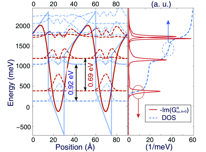
We perform a full quantum modelling of the effects of 3-D IFR within the framework of non-equilibrium Green’s functions Wacker and Jauho (1998); Lee and Wacker (2002); Rammer (1991). The model is explained as follows. The general Hamiltonian can be written as . The non-interacting includes the effective mass Hamiltonian within kp theory Sugawara et al. (1993), i.e. the superlattice potential assuming ideally smooth interfaces. The nonlinear spontaneous and piezoelectric polarization potentials are also contained in . is separable and can be diagonized straightforwardly, whose eigen-system is known as the Wannier-Stark (WS) basis. The wave functions of a WS state is expressed as , where the index represent the confined states in the out-of-plane direction , stands for the in-plane coordinates, and represents the in-plane momentum. An example of such a structure is shown in Fig. 1 (left part, blue curves). The interacting term includes electron-phonon interaction, impurity scattering and electron-electron interaction, respectively. represents the IFR random potential. The matrix element of in the WS basis is denoted as .
The characteristics of the structure are obtained by solving the Dyson equation
| (1) | ||||
where is energy, is the matrix element of , is the Kronecker delta, is the retard Green’s function, represents various self-energies. Repeated indices are summed. The terms in (1) are explained as follows. and are self-energies of electron-phonon interaction and impurity scattering, respectively. They are calculated with the Fock-type diagram in self-consistent Born Approximation (SCBA) Rammer (1991). The electron - electron Coulomb interaction is treated in the mean field approximation, i.e. Poisson equation; and is the mean-field potential calculated from
| (2) |
where is the permittivity, , is the Fermi-Dirac distribution, and is the density of the ionized impurities.
and in the Dyson equation (1) are IFR originated self-energies:
| (3) |
| (4) |
where angle brackets are understood as the configurational average. corresponds to the “single leg” diagram of random potential scattering. is the scattering self-energy induced by IFR, which is handled within SCBA. The expressions of and depend on .
Generically, the IFR stochastic potential is a 3-D function:
| (5) |
where is the band offset at the interface, is the ’s interface position, , is the Heaviside function, and is the interface fluctuation at the in-plane location of the interface. In (5) we retain the original form of the IFR stochastic potential with explicit 3-D dependence, and the approximation of a purely 2-D IFR potential is dropped.
is a Gaussian random process Khurgin (2008) with a probability distribution density and a correlation as
| (6) |
where is the roughness height, is the correlation length, and . Furthermore, the joint probability density at and is
| (7) |
where is the correlation matrix, and are the identity matrix and the -Pauli matrix, respectively.
With the original 3-D form of IFR potential retained in (5), can be expressed as 111See the supplementary material for the detailed derivation of .
| (8) |
where
| (9) |
and is the cumulative probability distribution. is the error function.
If a 2-D IFR potential is assumed, the “single leg” diagram of would produce an universal constant zero, thus has no physical effect. We recognize as precisely the unperturbed superlattice potential with ideally smooth interfaces. can be merged into , retaining the separability of the Hamiltonian. We call the basis formed by the eigenstates of the “proper-WS” basis.
We have plotted an example of the superlattice potential added with in Fig. 1 (left part, red curves). It is observed that inclusion of leads to an effective interface grading. As a result, the depths of the wells are reduced, causing a narrowing in the proper-WS subband energy spacing.
Without IFR, the polarization charges are localized on the ideal interface planes. However, due to roughness they are now distributed in . This induces a correction to the polarization fields close to the interfaces, followed by a small change of 30 meV in the ISB transition energies in these samples. This effect by itself does not explain the large energy ISB transition energy shift, but is included for accuracy in our calculation.
The IFR scattering self-energy introduced in (4) plays a vital role in the broadening and transport characteristics in the superlattice, and it can also contribute to the energy renormalization of the subbands. Based on the 3-D form of the IFR stochastic potential, can be expressed as Note (1)
| (10) | ||||
where , is the joint probability distribution found in (7), and the domain of integration is
| (11) |
To retrieve the energy structure of the superlattices, the Dyson equation (1) and the Poisson equation (2) are calculated iteratively. An example of the calculated imaginary part of the Green’s functions are plotted in Fig. 1 (right part), which represents the respective density of states (DOS) for each proper-WS subband state. Broadening in each subbands is discernable. The total DOS, is also plotted in Fig. 1. The staircase shape of the total DOS is a signature of a 2-D system, with the onset of each step corresponding to each proper-WS subband. Based on the calculated Green’s functions, the ISB transition spectrum can be generated by calculating the real part of the conductivity using the Kubo formula Rammer (1991); Ando (1978)222Here we retain full instead of the approximation of using the “on-shell” .
For a systematic study of the effect of 3-D IFR in the subband structure, we have designed, grown and characterized a series of GaN/Al(Ga)N superlattices with varying parameters listed in Table 1. All samples are grown by metal organic chemical vapor deposition (MOCVD) on c-plane sapphire. Multi-layered templates are employed, with the final layer being strain relaxed AlxGa1-xN matching to the average Al concentration in the active layers, ensuring balanced strain in the superlattices. The average layer thicknesses are controlled within 3.5% of the designed values. Multiple samples ( 3) are grown for the same designs to ensure repeatability. To compare to the theoretical results, an experimental estimation of the roughness height is obtained through characterization of the top surface morphology. To this end, atomic force microscope (AFM) measurements are performed at multiple locations and over multiple wafers. The result gives an average roughness height of 6 Å with a standard error of 2 Å.
| Sample | GaN (nm) | AlN (nm) | Doping ( cm-3) |
|---|---|---|---|
| A1 | 1.5 | 3.0 | 0.8 |
| A2 | 1.5 | 3.0 | 1.6 |
| A3 | 1.5 | 3.0 | 3.2 |
| B | 2.0 | 5.0 | 1.6 |
| C | 3.0 | 5.0 | 1.6 |
| D | 3.0 | 3.0 (Al0.6Ga0.4N) | 0.8 |
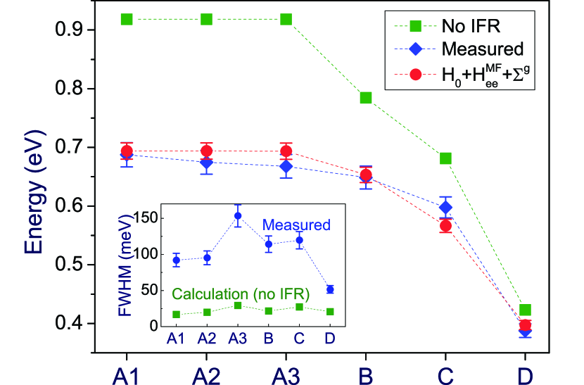
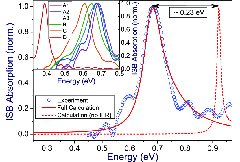
In Fig. 2 we have plotted the measured ISB absorption spectrum of design A1 (blue circles), the baseline spectrum calculated without the effects of IFR (dashed red curve) and that obtained in the full calculation (red solid curve). The observed ISB absorption only appears in the transverse magnetic polarization, which is a signature of ISB transition. The relevant material parameters used in the calculation are found in Ref. Morkoç (2009); *JP_Book2007nitride. The measured peak transition energy at 0.69 eV display a 0.23 eV red-shift from the baseline calculation. Conversely, with the effects of 3-D IFR included, the full calculation successfully reproduces both the peak transition energy and the broadening of the experimental result. The the measured ISB absorption spectra of all the designs in Table 1 are plotted in the inset of Fig. 2. The measured peak transition energies span 0.39 eV - 0.69 eV. A summary of the measured peak energies (purple) and that of the baseline calculation without considering the IFR effects (green) are shown in Fig. 3. To demonstrate the effect of the effective grading potential, the peak ISB transition energies calculated with and an universally fitted roughness height of 5.5 Å are also shown in Fig. 3 (red). All measured ISB transitions exhibit clear red-shift of up to 25% compared to the results from the baseline calculation. The deviation in the average layer thickness of 3.5 % can only lead to a energy shift of less than 20 meV, which can not account for such a significant discrepancy. The electron-electron and electron-ionized impurity interactions in these structures merely contribute to 5 meV of energy shift in the subbands, and is thus not the main reason for the observed discrepancy either. Contrarily, the calculation equipped with immediately brings the predicted ISB transition energies close to the experimental results, which is a clear evidence of the effect of the 3-D IFR. This reaffirms the reduction of energy spacings between the proper-WS subbands observed in Fig. 1.
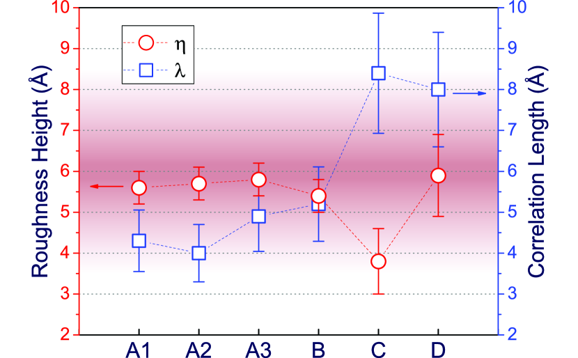
The measured full width at half maximum (FWHM) of the ISB transitions, originated from the broadening of the proper-WS subbands, ranges from 50 meV to 150 meV (13% - 23% of the transition energy) in different designs. A summary is shown in the inset of Fig. 3. Such values are significantly larger than those found in the III-phosphide or -arsenide material system. For a comparison, the calculated FWHM without the IFR effects are also plotted in the inset. The resulting broadening is merely 20% - 40% of the measured FWHM, clearly indicating the importance of the missing factor of the IFR scattering. With the full theoretical model developed above, one can extract the roughness height and the correlation length in each sample by fitting to the peak position and the FWHM of the ISB transition spectra. A summary of the extracted and is shown in Fig. 4. The experimental estimation of the roughness height is also indicated in the shaded region in Fig. 4. All fitted reside within the range of experimental results. For the correlation length , proper experimental measurement methods are still under discussion, with large uncertainty found in the reported values (14 Å 120 Å) for the more studied materials Gold (2008); Khurgin (2008); Luhman et al. (2007); Quang et al. (2009). It is worthy to note that in this work the energy shift and the broadening provide two constraints, which enables simultaneous fitting of and . The resulting correlation length ranges from 4 Å to 10 Å. The variation among samples A-D is understandable since they have different structure designs and are grown on templates with different material compositions. The correlation lengths found here are generally smaller than those in III-phosphide or -arsenide material system; this meets our expectation given that the interfaces in III-nitride materials are known to be considerably rougher.
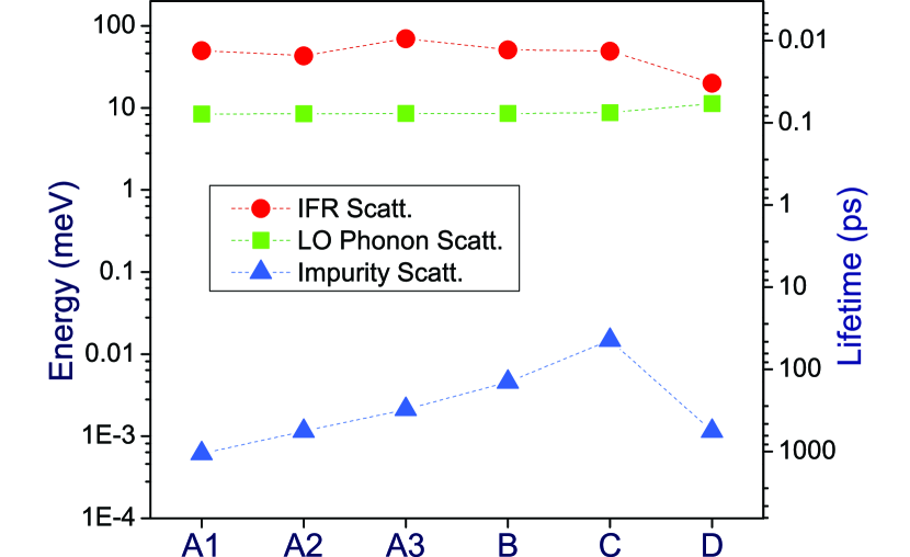
In Fig. 5 we have plotted the semi-classical lifetimes of 3-D IFR, LO phonon and impurity scattering to illustrate their relative importance in the proper-WS subband broadening Lee and Wacker (2002). As is shown, LO phonon scattering lifetimes are typically 0.05 ps, while that of impurity scattering is 50 ps. Again, clear dominance of the IFR scattering of 0.01 ps is observed, a result of strong 3-D IFR in thin QWs.
In summary, we have developed a general model for treating the effect of 3-D IFR in thin layered semiconductor structures. An effective grading potential is predicted in the model, which significantly alters the energy spectrum and leads to a narrowing in the subband spacing. The IFR scattering self-energy is also derived for the general case, and the IFR scattering mechanism is shown to be dominant over phonon and impurity scattering. Through the full calculation, the anomalous energy shift and the significant broadening observed in the ISB transitions are explained. Beyond the optical transitions, the results in this work are also applicable to the vertical as well as in-plane transport studies. Investigations of similar IFR effects in structures of other dimensions such as quantum wires and quantum dots are also enabled. Equipped with the quantitative results of this work, the ISB light emission in III-nitride superlattices in the mid-infrared wavelength range is realized Song et al. (2014, ).
Acknowledgements.
This work is supported in part by MIRTHE (NSF-ERC). The authors would like to thank Dr. Joesph Maciejko for valuable discussions.References
- Miao et al. (2012) M. S. Miao, Q. Yan, C. G. Van de Walle, W. K. Lou, L. L. Li, and K. Chang, Physical review letters 109, 186803 (2012).
- Takagi et al. (2013) H. Takagi, H. Kunugita, and K. Ema, Physical Review B 87, 125421 (2013).
- König et al. (2007) M. König, S. Wiedmann, C. Brüne, A. Roth, H. Buhmann, L. W. Molenkamp, X.-L. Qi, and S.-C. Zhang, Science 318, 766 (2007).
- King et al. (2012) P. King, R. He, T. Eknapakul, P. Buaphet, S.-K. Mo, Y. Kaneko, S. Harashima, Y. Hikita, M. Bahramy, C. Bell, et al., Physical review letters 108, 117602 (2012).
- Kuch et al. (2006) W. Kuch, L. Chelaru, F. Offi, J. Wang, M. Kotsugi, and J. Kirschner, Nature Materials 5, 128 (2006).
- Almeida et al. (2014) R. A. L. Almeida, S. O. Ferreira, T. J. Oliveira, and F. D. A. Aarão Reis, Physical Review B 89, 045309 (2014).
- Boullay et al. (2011) P. Boullay, A. David, W. Sheets, U. Lüders, W. Prellier, H. Tan, J. Verbeeck, G. Van Tendeloo, C. Gatel, G. Vincze, et al., Physical Review B 83, 125403 (2011).
- Edmunds et al. (2013) C. Edmunds, L. Tang, M. Cervantes, M. Shirazi-HD, J. Shao, A. Grier, A. Valavanis, J. D. Cooper, D. Li, G. Gardner, D. N. Zakharov, Z. Ikonić, D. Indjin, P. Harrison, M. J. Manfra, and O. Malis, Phys. Rev. B 88, 235306 (2013).
- Nakagawa et al. (2006) N. Nakagawa, H. Y. Hwang, and D. A. Muller, Nature materials 5, 204 (2006).
- Santamaria et al. (2002) J. Santamaria, M. E. Gómez, J. L. Vicent, K. M. Krishnan, and I. K. Schuller, Physical review letters 89, 190601 (2002).
- Chevoir and Vinter (1993) F. Chevoir and B. Vinter, Physical Review B 47, 7260 (1993).
- Ando et al. (1982) T. Ando, A. B. Fowler, and F. Stern, Rev. Mod. Phys. 54, 437 (1982).
- Brunner et al. (1994) K. Brunner, G. Abstreiter, G. Böhm, G. Tränkle, and G. Weimann, Applied physics letters 64, 3320 (1994).
- Leosson et al. (2000) K. Leosson, J. R. Jensen, W. Langbein, and J. M. Hvam, Physical Review B 61, 10322 (2000).
- Bayram et al. (2009) C. Bayram, N. Péré-laperne, and R. M., Appl. Phys. Lett. 95, 201906 (2009).
- Machhadani et al. (2013) H. Machhadani, M. Beeler, S. Sakr, E. Warde, Y. Kotsar, M. Tchernycheva, M. P. Chauvat, P. Ruterana, G. Nataf, P. De Mierry, E. Monroy, and F. H. Julien, Journal of Applied Physics 113, 143109 (2013).
- Lee et al. (2009) M. Lee, M. O. Hachiya, E. Bernardes, J. C. Egues, and D. Loss, Physical Review B 80, 155314 (2009).
- Wacker and Jauho (1998) A. Wacker and A.-P. Jauho, Phys. Rev. Lett. 80, 369 (1998).
- Lee and Wacker (2002) S.-C. Lee and A. Wacker, Phys. Rev. B 66, 245314 (2002).
- Rammer (1991) J. Rammer, Reviews of Modern Physics 63, 781 (1991).
- Sugawara et al. (1993) M. Sugawara, N. Okazaki, T. Fujii, and S. Yamazaki, Phys. Rev. B 48, 8102 (1993).
- Khurgin (2008) J. B. Khurgin, Applied Physics Letters 93, 091104 (2008).
- Note (1) See the supplementary material for the detailed derivation of .
- Ando (1978) T. Ando, Journal of the Physical Society of Japan 44, 765 (1978).
- Note (2) Here we retain full instead of the approximation of using the “on-shell” .
- Morkoç (2009) H. Morkoç, “Electronic band structure and polarization effects,” in Handbook of Nitride Semiconductors and Devices (Wiley-VCH Verlag GmbH & Co. KGaA, 2009) pp. 131–321.
- Piprek (2007) J. Piprek, Nitride semiconductor devices: principles and simulation (John Wiley & Sons, 2007).
- Gold (2008) A. Gold, Journal of Applied Physics 103, 043718 (2008).
- Luhman et al. (2007) D. Luhman, D. Tsui, L. Pfeiffer, and K. West, Applied Physics Letters 91, 072104 (2007).
- Quang et al. (2009) D. N. Quang, N. H. Tung, L. Tuan, N. T. Hong, and T. T. Hai, Applied Physics Letters 94, 072106 (2009).
- Song et al. (2014) Y. Song, R. Bhat, P. Badami, T.-Y. Huang, Z. Chung-En, and C. F. Gmachl, in CLEO: Science and Innovations (Optical Society of America, 2014) pp. STh4I–2.
- (32) A. Y. Song, R. Bhat, A. A. Allerman, J. Wang, T.-Y. Huang, C.-E. Zah, and C. F. Gmachl, in preparation .