Tunneling conductance in half-metal/conical magnet/superconductor junctions in the adiabatic and non-adiabatic regime: self-consistent calculations
Abstract
The tunneling conductance in the half-metal/conical magnet/superconductor (HM/CM/SC) is investigated by the use of the combined Blonder-Tinkham-Klapwijk (BTK) formalism and the Bogoliubov-de Gennes (BdG) equations. We show that the conductance calculated self-consistently differs significantly from the one calculated in the non-self-consistent framework. The use of the self-consistent procedure ensures that the charge conservation is satisfied. Due to the spin band separation in the HM, the conductance in the subgap region is mainly determined by the anomalous Andreev reflection the probability of which strongly depends on the spin transmission in the CM layer. We show that the spin of electron injected from the HM can be transmitted through the CM to the SC adiabatically or non-adiabatically depending on the period of the exchange field modulation. We find that the conductance in the subgap region oscillates as a function of the CM layer thickness wherein the oscillations transform from irregular, in the non-adiabatic regime, to regular in the adiabatic case. In the non-adiabatic regime the decrease of the exchange field amplitude in the CM leads to the emergence of the conductance peak for one particular CM thickness in agreement with experiment [J.W.A Robinson, J. D. S Witt and M. G. Blamire, Science 329, 5987]. For both transport regimes the conductance is analyzed over a broad range of parameters determining the spiral magnetization in the CM.
I Introduction
In recent years the quantum transport in the ferromagnet/superconductor (FM/SC) junctions has attracted growing interest due to a possible existence of the spin-triplet pairingChampel and Eschring (2005); Braude and Nazarov (2007); Houzet and Buzdin (2007); L ofwander et al. (2007) and novel transport phenomena related to this unique superconducting state.Buzdin (2005); Bergeret et al. (2005) For the s-wave superconductors with the spatially symmetric orbital part of the Cooper pair wave function, the Pauli principle requires that its spin part is antisymmetric, which means that the spin-singlet seems to be the only possible state for the Cooper pair. However, many years ago BerezinskiiBerezinskii (1974) proposed a possible existence of the spin-triplet state in a system with the s-wave interaction which do not violated the Pauli principle. The triplet pairing correlations proposed by Berezinskii are odd in time (or frequency) and can appear in systems with sort of the time-reversal symmetry breaking mechanism. Recent studies suggest that the spin-triplet Cooper pair correlations can be induced and observed experimentally in the FM/SC junctions with the spin-active or magnetically inhomogeneous interface.Bergeret et al. (2001, 2003); Volkov et al. (2003)
In the normal metal/superconductor (NM/SC) junctions the electrons incident on the interface from the NM side are reflected as holes with opposite spins. This mechanism, known as the Andreev reflection,Andreev (1964) leads to the proximity effect - the superconducting pairing correlations penetrate into the normal metal over the distance as long as one micron at low temperature.Lambert and Raimondi (1998) The proximity effect significantly changes if we replace the normal metal by the ferromagnet. The exchange interaction in the ferromagnet results in the different Fermi wave vectors for electrons with opposite spins forming the Cooper pairs. This wave vector mismatch is compensated by the non-zero total momentum of the electron pairs giving rise to the oscillations of the spin-singlet superconducting correlations in the ferromagnet,Buzdin (2005); Demler et al. (1997) known as the FFLO oscillations.Fulde and Ferrell (1964); Larkin and Ovchinnikov (1964) Since the exchange field tends to align the electronic spins along the field direction, the spin-singlet superconducting correlations in the ferromagnet are strongly suppressed leading to the short-range penetration length. In contrast to the short-range proximity effect for the spin-singlet state, the spin-triplet state with , with both electronic spin of the Cooper pair directed along the exchange field, is robust against the pair breaking induced by the exchange interaction. Therefore, the spin-triplet superconducting correlations (), if they exist, can penetrate the ferromagnet over the distance comparable to this observed in the NM/SC junctions. This phenomenon, called long-range proximity effect was predicted theoretically by Bergeret et al. (see Refs. Bergeret et al., 2001, 2003, 2005). It was foundBergeret et al. (2001, 2003, 2005) that in the FM/SC multilayer junctions with the spin-active or magnetically inhomogeneous interface (the spin-flip processes are possible) all three components and of the spin-triplet state can arise. Despite few theoretical studies on the spin-triplet pairing induced by the spin-active interface, including the effect of domain wall,Fominov et al. (2005) spin-orbit couplingLv. (2011) or spin-dependent potential,Terrade et al. (2013) up to date, the direct evidence of the spin-triplet supercurrent has been observed in multilayer FM/FM/SC systems with a non-collinear magnetization of the ferromagnetic layers.Klose et al. (2012); Gingrich et al. (2012); Leksin et al. (2012)
A first experimental hint for the long-range proximity effect was reported in a half-metal Josephson junction based on CrO2.Keizer et al. (2009) However, since the measured critical current varied by two orders of magnitude in similar samples, the results of this experiment needed to be confirmed. The strong evidence for the long range proximity effect was then reported in the Josephson junctions based on Co.Khaire et al. (2010) The dependence of the critical current on the Co layer thickness, which agrees with the theoretical expectations, provides a strong experimental confirmation of the existence of the spin-triplet pairing in the FM/SC heterojunctions. Further studies on the spin-triplet pairing concerned the FM/SC/FM and FM/FM/SC junctions with a relative magnetization between the ferromagnets. The spin triplet pairing in the clean FM/SC/FM nanostructures with an arbitrary angle between the magnetization of the FM layers was theoretically studied by Haltermann et al. in Refs. Halterman and Valls, 2005; Halterman et al., 2007, 2008; Zhu et al., 2010. The authors used the self-consistent solutions of the microscopic Bogoliubov de-Gennes (BdG) equations and analyzed the spin-triplet correlations as a function of the relative magnetization between the magnets. The self-consistent calculations allowed to confirm the experimentally observed angular dependence of the critical temperature which monotonically increases due to the presence of the long range spin-triplet correlations. reaches minimum if the relative magnetization is parallel and maximum for antiparallel magnetization.Zhu et al. (2010) A different behavior was observed for the FM/FM/SC nanostructures for which the critical temperature is minimized in case of perpendicular alignment of the magnetization.Leksin et al. (2011); Wu et al. (2012a)
Research on the spin-triplet pairing in the FM/FM/SC junctions has been recently extended to systems with the conical (helical) ferromagnets (CM). Efforts to control the long-range triplet supercurrent has been recently demonstrated in Josephson junctions based on holmium(Ho)-Cobalt(Co)-holmium(Ho) multilayer setup.Robinson et al. (2010) One has been observed a nonmonotonic dependence of the critical supercurrent as a function of the Ho layer thickness, , with peaks for nm and nm. By increasing the Co layer thickness a slow decay of the critical current has been reported in agreement with theoretical calculations. Alidoust and Linder (2010) Nevertheless, the theoretical model presented in Ref. Alidoust and Linder, 2010 does not explain the complex dependence of the critical supercurrent on the Ho thickness. The nonmonotonic behavior of has been obtained by Halász et al. in Ref. Halász et al., 2011 who have performed calculations in the clean limit using Eliashberg equations. Similar dependence has been also demonstrated by the use of the Blonder-Tinkham-Klapwijk (BTK) approach.Wen et al. (2014); Jin et al. (2012)
In the mentioned theoretical worksHalász et al. (2011); Wen et al. (2014); Jin et al. (2012) the proximity effect at the CM/SC interface has been neglected meaning that the superconducting pair potential has been assumed to be a step function. However, as shown by recent studies,Wu et al. (2014) only the self-consistent calculations of the tunneling conductance guarantees that the charge conservation law is satisfied. It means that one cannot properly determine the tunneling conductance in the FM/CM/SC heterostructures by using the non-self-consistent framework. The full self-consistent approach is needed. The self-consistent calculations of the spin-triplet correlations in two layered CM/SC junctions have been presented in Refs. Wu et al., 2012b, c. Nevertheless, these studies concern only the spin-triplet correlations between the CM and SC. They do not include the analysis of the tunneling conductance (transport calculations), the influence of the FM layer attached to the CM or the influence of the CM layer thickness. Summing up, the theoretical analysis of the tunneling conductance through the FM/CM/SC heterojunctions with the inclusion of the proximity effect in the full self-consistent framework has not been presented until now.
In the present paper we report the full self-consistent calculations of the tunneling conductance in the HM/CM/SC junctions. The charge transport in the considered system is mainly determined by the anomalous Andreev reflection, the probability of which strongly depends on the spin transmission in the CM layer. We consider the conductance in two cases in which the spin transport is adiabatic and non-adiabatic. The conductance is analyzed over a broad range of parameters determining the spiral magnetization in the CM. We show that the tunneling conductance in the HM/CM/SC junctions strongly depends on the spin transport regime. The paper is organized as follows: in Sec. II we introduce the basic concepts of the theoretical scheme based on the self-consistent solution of the BdG equations and the BTK formalism. In Sec. III we present the results while the summary is included in Sec. IV.
II Theoretical method
We consider the FM/CM/SC structure schematically illustrated in Fig. 1. In the plane the system is assumed to be infinite while the axis is perpendicular to the layers whose lengths are denoted by , , , respectively.
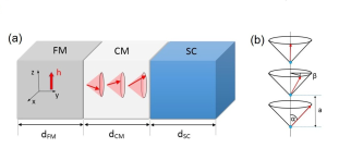
The value and the direction of the exchange field , denoted by the red arrow in Fig. 1, depends on the position. It is directed along the axis in the ferromagnet, , while, in the conical ferromagnet, is given by
| (1) |
where is the exchange field amplitude, determines the angle of a relative magnetization of the CM layer measured from the FM layer at the FM/CM interface while and are the cone and rotation angle whose physical meaning is depicted in Fig. 1(b). From Eq. (1) the spatial period of the helix exchange field is , where is the lattice constant.
In the present paper we consider the charge transport through the FM/CM/SC junction and analyze the tunneling conductance as a function of the system parameters. As mentioned above, the correct analysis of the conductance behavior require the inclusion of the proximity effect. This can be done only by the full self-consistent calculations in which the pair potential distribution is determined from the microscopic BdG equations. The self-consistent procedure used in the paper consists of two steps. First, we determine the self-consistent pair potential in the nanostructure by solving BdG equations. Then, is used to calculate the tunneling conductance within the BTK approach. Blonder et al. (1982); Bugoslavsky et al. (2005); Wójcik et al. (2011) Below, both these steps are described in detail.
II.1 Self-consistent pair potential calculations
The effective BCS Hamiltonian of the considered system is given by
| (2) | |||||
where , are the creation and annihilation operators with spin , is the exchange field, is the Pauli matrices vector, is the chemical potential and is the spin-singlet pair potential in real space defined as
| (3) |
where is the phonon-mediated electron-electron coupling constant. The generalized Bogoliubov transformation
| (4) |
where and are the quasiparticle annihilation and creation operators, and are the electron and hole components of the amplitudes vector and for spin down(up), reduces the Hamiltonian (2) into the diagonal form. By the commutation relation
| (5) |
| (6) |
where is the single electron Hamiltonian, and using the fact that the system is infinite in the plane we obtain the BdG equations in the quasi-one dimensional form
| (7) |
Equations (7) are coupled with the expression for the pair potential given by
| (8) | |||||
where is the Fermi-Dirac distribution. The summation in
Eq. (8) is carried out only over the electronic states with energy inside the
Debye window , where is the Debye frequency.
In our approach is assumed to be nonzero only in the SC layer.
The self-consistent procedure used to solve the BdG equations (7) is similar to these reported in previous papers.Wu et al. (2012b); Halterman and Valls (2005); Halterman et al. (2007, 2008) The main difference is that the assumed basis functions have the form of the plane waves. Such choiceis needed in the transport calculations because it guarantees nonzero current at the boundaries of the system. The self-consistent procedure can be described as follows. First, the BdG equations (7) are diagonalized in the basis of the plane waves
| (9) |
where are the expansion coefficients, is the wave vector with being an integer while is the total length of the nanostructure. Then, using the calculated wave functions the new pair potential is determined on the basis of Eq. (8). This new distribution is used in the next iteration in which we again solve the BdG equations and determine . This procedure is repeated until the convergence is reached. Due to the high computational complexity of such scheme the parallel implementation of the numerical procedure is required.
Finally, we also calculate the magnetization vector given by the formula
| (10) | |||||
| (11) | |||||
| (12) | |||||
where are the Bohr magneton.
II.2 Tunneling conductance calculations
The tunneling conductance calculations have been performed within the tight-binding approximation using the Kwant package.Groth et al. (2014) For this purpose we have transformed the BdG equations (7) into the discretized form on the grid with lattice constant (). We introduce the discrete representation of the quasi-particle wave vector as follows: , Introducing a set of Pauli-like matrices in electron-hole space, the discretized tight-binding form of the Hamiltonian in Eq.(7) is given by
where , , and is the unity matrix.
Let us assume that the electron with
spin-up is injected from the FM into the SC through the CM layer. There are five possible
scattering processes: normal reflection with spin conservation ,
normal reflection with spin-flip , reflection as a hole with
opposite spin (normal Andreev reflection, ), reflection as a hole with
spin conservation (anomalous Andreev reflection, ) and transmission as
a quasi-particle . In the above, denotes the reflection probability where upper and lower right index
corresponds to the state of an incident particle while upper and lower left index is associated
with the reflected one, is the transmission probability where upper indexes indicate
the state of incident particle. Analogous scattering processes can be distinguished for the
spin-down electron injected from the FM. Their probabilities are marked by , , , and , respectively.
According to the BTK approach the current through the FM/CM/SC junction can be calculated from the
formula
| (14) |
where is the bias voltage and is the Fermi-Dirac distribution. At low temperature the energy dependent tunneling conductance (in units of ) is given by
| (15) | |||||
where , expressed in units of , corresponds to the spin polarization at the Fermi level in the FM layer. In our calculations the reflection probabilities in Eq. (15) are determined by the use of the Kwant packageGroth et al. (2014) which requires the implementation of the discretized tight-binding Hamiltonian given by Eq. (II.2). In the paper, we consider the forward tunneling conductance with the angle of the incident electron and neglect the scattering potential at the interfaces.
III Results and discussion
In this section we analyze the tunneling conductance through the FM/CM/SC junctions by the use of the full self-consistent approach presented in Sec. II. Since the first experimental evidence for the long-range proximity effect (spin-triplet pairing) was reported in a half-metal Josephson junction,Keizer et al. (2009) we restrict our analysis to the case in which the ferromagnetic layer is embedded in a half-metal (HM), . In our calculations we neglect the Fermi wave-vector mismatch between the layers assuming a constant value of the chemical potential throughout the nanostructure. Its value is used as the energy unit. In the calculations we adopt the following values of the parameters: zero temperature energy gap in the bulk , Debye energy , temperature and the lattice constant nm corresponding to the conical magnet Holmium.Robinson et al. (2010) Other parameters determining the magnetic configuration of the MC, namely the exchange field amplitude , the cone angle , the rotation angles and , as well as the CM layer thickness are used to analyze the tunneling conductance through the HM/CM/SC junctions and vary from one simulation to another.
As predicted by Bergeret et al.Bergeret et al. (2001, 2003) the join effects of the Andreev reflection and the proximity at the FM/SC interface allow for the coexistence of the spin-singlet pairing correlations and the spin-triplet pairing correlations with the total spin projection ). If a magnetically inhomogeneous layer, such as the CM layer, is present between the FM and SC, the spin-triplet state with can be rotated to the state with (). It means that the existence of the spin-triplet pairing with strongly depends on the spin transmission in the CM layer. This, in turn, is determined by the exchange field which in the CM has a rotating component varying with the period . Depending on the spins of electrons injected from the FM can be transmitted through the CM adiabatically - the spin orientation follows the spatial modulation of the exchange field, or non-adiabatically - the period of the exchange field modulation is so short that the electron spin is not able to adopt to the field changes. The degree of adiabaticity can be defined by the parameter , where is the magnetic field modulation frequency in the electron’s frame of reference, is the Fermi velocity and is the frequency of the spin Larmor precession. In the adiabatic regime, . Below, we analyze the tunneling conductance through the HM/CM/SC junctions in both adiabatic and non-adiabatic regimes.
III.1 Non-adiabatic regime
All results presented in this subsection have been obtained for the rotational angle which corresponds to the spatial period of the helical exchange field nm measured in the Holmium.Robinson et al. (2010) For this value of the spin transport through the considered system is non-adiabatic, .
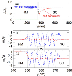
In Fig. 2 we present the pair potential and the magnetization in the nanostructure calculated for , and the thickness of the conical magnet layer nm. As shown in Fig. 2(a) the self-consistent pair potential significantly differs from the one used in the non-self-consistent approach. Due to the proximity effect does not have the step-like form but smoothly increases in the SC region reaching its bulk value for a distance grater than the coherence length. Similarly, as the magnetism alters the superconductivity near the CM/SC interface, the superconductivity also influences the magnetism. This so-called reverse proximity effect allows to penetrate the magnetization into the SC region as presented in Fig. 2(b,c). Almost a tenfold reduction of the magnetization amplitude in the CM layer (red lines), as compared to the exchange field (blue dashed lines), results from the fact that the chosen value of corresponds to the non-adiabatic transport regime. In this regime the changes of the exchange field seen by electrons flowing through the nanostructure are so fast that the their spin do not have enough time to adopt to these changes. As a result, the electron spin rotates around the exchange field irregularly. Note that, in accordance with Eqs. (10)-(12), the magnetization is expressed as a sum of the averaged spin over states with different wave vectors. Since spins of these states rotate around with different irregular frequency, this sum averages to low value. In subsection B we will show that the suppression of the magnetization does not dependent on the conical magnet thickness but, as expected, is mainly determined by the spatial period of the helical exchange field .
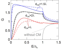
For the self-consistent pair potential we calculate the tunneling conductance using the procedure described in Sec. II B. Figure 3 presents the normalized conductance as a function of energy for different thicknesses of the CM layer calculated by the use of the non-self-consistent (dashed lines) and the self-consistent (solid lines) procedure. For comparison, we also mark the conductance calculated without the CM (gray lines). As we see the dashed and solid gray lines overlap which results from the fact that the conductance in this case is nonzero only for the high-energy limit, above the energy gap, for which the electron incident into the superconductor does not experience much difference between the step-like pair potential and the smooth pair potential from the self-consistent approach. Results presented in Fig. 3 clearly show that the self-consistent conductance is considerably different than this obtained in the non-self-consistent framework. The most pronounced difference between them is observed in the subgap energy range. Based on the results presented in Fig. 2 and 3 one can formulate the following conclusion: to properly determine the tunneling conductance in the HM/CM/SC heterojunctions the full self-consistent calculations including the proximity effect are needed.
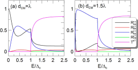
To explain the conductance behavior presented in Fig. 3 let us first discuss the half-metal/superconductor (HM/SC) junctions without the CM layer. In the HM/SC junctions the normal Andreev reflections are forbidden due to the isolation of the spin band. This leads to the zero conductance in the subgap energy regime as depicted by the gray solid lines in Fig. 3 (we assume no scattering potential at the interface). The situation diametrically changes if we put the conical magnet between the HM and SC. As predicted by Bergeret et al.Bergeret et al. (2001, 2003) the magnetic inhomogeneity at the FM/SC interface can induce the non-zero correlations of all three components and of the spin-triplet state. As a consequence, one appears an extra scattering mechanism, called the anomalous Andreev reflection in which electron incident into the SC is reflected as a hole with the same spin (in contrast to the normal Andreev reflection in which the incident electron and the reflected hole have opposite spins). For the HM/CM/SC junctions, this new scattering mechanism, if it exists, leads to the nonzero conductance in the subgap region as presented in Fig. 3. As one can see the conductance strongly depends on the thickness of the conical magnet layer, , i.e. its value reaches minimum for and maximum for , respectively. In Fig. 4 we present the reflection and transmission probabilities , , , , as a function of energy for these two distinguished thicknesses. We see that for the CM thickness the increase of the conductance in the subgap region is mainly determined by the increase of the anomalous Andreev reflection probability . On the other hand the probability is suppressed for for which the normal reflection with spin conservation emerges and also contributes to the conductance value leading to its decrease. Regardless of the CM layer thickness, for low energy, the anomalous Andreev reflection probability drops to zero while the normal reflection increases to unity. This results in the zero conductance at zero energy as demonstrated in Fig. 3.
Now, we discuss the thickness dependence of the conductance , important from the viewpoint of experiments in which the critical current is measured as a function of the CM layer thickness. In Fig. 5 we present the tunneling conductance as a function of energy and .
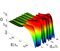
We see that the conductance oscillates as a function of the CM layer thickness with the amplitude which is not constant but varies wit . The clear evidence of these oscillations is shown in Fig. 6(b) where the cross-section of the map is presented for the energy . The small number of points in this figure results from the high computational cost of the full-self consistent calculations. Results presented in Fig. 6 (b) are consistent with the phenomena observed in experiments, namely (i) the conductance is a nonmonotonic function of with peaks for the half-integer multiplies of and (ii) the conductance slowly decays with increasing CM layer thickness. For comparison, in Fig. 6(a) the non-self-consistent dependence for are also presented. As we see the peaks in conductance calculated in the non-self-consistent framework are greater than the corresponding peaks calculated self-consistently. Moreover, the conductance decay rate (with increasing ) is slower than in the self-consistent approach.
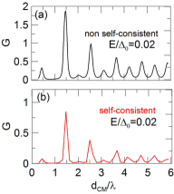
The irregular nonmonotonic dependence of the conductance presented in Figs. 5 and 6 can be explained as follows. If the spin-active region (the CM layer) is present at the FM/SC interface the anomalous Andreev reflections can appear giving raise to the nonzero conductance in the subgap region. Bergeret et al. (2001, 2003) The probability depends mainly in the spin transition in the CM layer. Note, that the strength of the spin-flip scattering in the CM is proportional to the off-diagonal matrix elements of the Hamiltonian (7) which have the form . Since and vary periodically, the strength of the spin-flip scattering also oscillates with increasing CM layer thickness. Nevertheless in the non-adiabatic regime the modification of the exchange field seen by electrons flowing through the nanostructure is so fast that the electronic spins are not able to follow these changes. It entails the irregular oscillations of the anomalous Andreev reflection probability and, in consequence, the irregular oscillations of the conductance depicted in Figs. 5 and 6.
In delineating the role of the spin-triplet pairing in the charge transport through the HM/CM/SC junctions, it is necessary to understand the behavior of the conductance under the influence of the magnetic configuration in the CM layer determined by the value of the exchange field amplitude and the angles and (see Eq. 1). In Fig. 7 we plot the conductance maps for the exchange field amplitude (a) and (b) . Other parameters are assumed to be the same as in previous calculations, results of which are presented in Fig. 5.
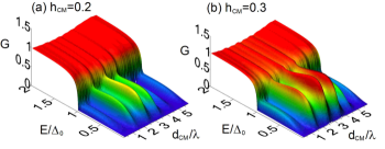
Figure 7 clearly demonstrates the suppression of the conductance in the subgap region with decreasing exchange field amplitude . The comparison of Fig. 7 and Fig. 5 allows to conclude that the strength of this conductance suppression depends on the CM layer thickness. It is minimal for . Note that, for the conductance peak for is still well pronounced [Fig. 7(a)]. Further reduction of the amplitude leads to the situation in which the conductance peak survives only for in consistency with the experimental measurements reporting the peak of the critical current exactly for this value of the CM layer thickness. Although the conductance for decreases slower than for other thicknesses, even for this value of the conductance in the subgap region is suppressed with decreasing . This suppression is depicted in Fig. 8 which presents for different values of the exchange field amplitude . We see that in the limit , as expected, the conductance in the subgap region tends to zero.
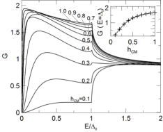
We should also notice clear cups in the conductance for the energy . The non-self consistent analysis for the FM/SC junctions without the CM layer leads to the analytical dependence of which is a decreasing function of the exchange field in the ferromagnetŽutić and Valls (2000)
| (16) |
As depicted in the insert of Fig. 8 for the HM/CM/SC junctions the dependence is an increasing function of in contrast to the FM/SC structure. This results from the fact that the conductance for the considered energy is mainly determined by the anomalous Andreev reflections whose probability increases with increasing amplitude of the spiral magnetic configuration in the CM layer.
The magnetic configuration in the CM layer can be modified not only by changing the amplitude but also by changing the spatial configuration determined by the angles , and . Figure 9(b) presents the conductance for different angles of a relative magnetization of the CM layer measured from the HM layer at the HM/CM interface.
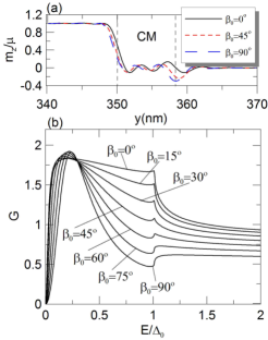
In panel (a) we present the -component of the magnetization for three different angles . Note that is not discontinuous but changes smoothly at the interfaces HM/CM and CM/SC. It saturates to unity in the HM region on the left-hand and penetrates the SC region on the right-hand. Although the amplitude of the exchange field is the same for all three cases, the conductance in the subgap region decreases with increasing [see Fig. 9(b)]. This behavior can be easily understood by considering two factors. The fist is directly related to the oscillatory dependence of the conductance with the CM layer thickness. In fact, the introduction of a relative magnetization between the HM and CM layers corresponds to the phase shift in the oscillatory dependence of the helical magnetic configuration. Therefore, in the first approximation, the dependence should be shifted in argument by . This shift causes the conductance for (corresponds to the maximum value for ) shifts to lower value related to . The second factor is the increase of the normal reflection probability at the HM/CM interface resulting from the discontinuity of the exchange field. The presented dependence is important in the simulation of the real HM/CM/SC structure since the conical magnets used in the multilayer setup have several ways to orient the magnetic moments with respect to the half-metal magnetization depending on the magnetic coupling at the HM/CM interface.
All results presented so far have been obtained for for which the -component of the exchange field is zero - the magnetization in the CM layer rotates in the plane. Now, we analyze the conductance for the non-zero value of . In Fig. 10 we plot the conductance map for two values of the cone angle (a) and (b) . We see that for the low cone angle the conductance map significantly differs from the map for (Fig. 5).
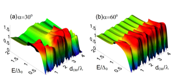
Based on Fig. 10 one can state that regardless of the angle the value of the conductance in subgap region oscillates as a function of whereas the period and the amplitude of these oscillations are irregular. In Fig. 11 we present the conductance map as a function of the cone angle calculated for the CM layer thickness (a) and (b) nm.
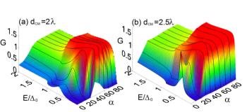
As we can see, the conductance in the subgap region decays with decreasing the cone angle, whereas the decay rate strongly depends on . For it is stronger than for .
III.2 Adiabatic regime
In this subsection we analyze the the tunneling conductance in the HM/CM/SC junctions in the adiabatic regime for a long period . In subsection III.1 we have demonstrated that in the non-adiabatic regime the magnetization in the CM layer is strongly suppressed compared to the helical exchange field. As presented in Fig. 2 (b,c) the amplitude of and modulation in the CM is about ten times smaller than the amplitude of the helical exchange field. Such a strong suppression have been obtained for a short period of the exchange field modulation nm corresponding to (non-adiabatic regime). It has been suggested that the magnitude of this suppression can be used as the additional parameter to measure the degree of adiabaticity.
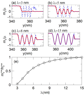

In Fig. 12 we demonstrate the self-consistent -component of the magnetization for different values of assuming . For comparison the distributions of the exchange field are plotted by the blue dashed lines. As presented in Fig. 12 (compare the red and blue lines), the suppression of the magnetization in the CM layer is more pronounced for a short period of the exchange field modulation (non-adiabatic regime) and almost completely disappears for a long (adiabatic regime). For nm there is no difference between the magnetization and the exchange field except the boundaries of the CM layer where smoothly changes penetrating the SC region due to the reverse proximity effect. Fig. 12 (e) presents the ratio of the amplitudes in the CM as a function of the exchange field modulation period . As one can see the ratio saturates to the value for grater than nm for which the transport through the heterojunction can be assumed to be adiabatic. The further analysis presented in this subsection will be carried out in the adiabatic regime for nm corresponding to .
Figure 13 shows the normalized conductance as a function of energy and CM layer thickness for the cone angles and . For corresponding to [Fig.13(c)] the conductance in the subgap region oscillates with a period . It reaches maximum for being an integer multiple of . In this case (we assume ) the spin of electrons injected from the HM has the same direction as the exchange field in the CM. In the adiabatic regime the spin of electrons flowing through the nanostructure follows the exchange field. Therefore, in this case the anomalous Andreev reflection probability is exactly proportional to the off-diagonal elements which oscillate leading to the regular oscillations of the conductance presented in Fig. 13(c). This behavior considerably differs from the irregular conductance oscillations presented in Fig 5 for non-adiabatic regime. Moreover, note, that the value of the conductance in the subgap region is lower than this obtained in the non-adiabatic regime (compare with Fig. 5) which is caused by the enhancement of the normal reflection probability due to increase of the exchange field modulation period .
For the cone angle , corresponding to the non-zero , the spin of electrons injected from the HM is non-collinear with the exchange field at the HM/CM interface. Therefore, the electronic spin starts to precesses around the exchange field direction with the Larmor frequency which, in the adiabatic regime, is much higher than the frequency of the exchange field modulation experienced by electrons flowing through the CM. For nm () one period of the exchange field modulation corresponds to ten full-rotations of electron spin around the exchange field direction. Therefore, for the non-zero the spin behavior in the CM layer is determined by joint effects: Larmor precession and the exchange field modulation. For certain energies and the CM thicknesses this complex spin behavior leads to the enhancement of normal reflection probability with spin flip presented in Fig. 14(b). Note, that the probability of this scattering mechanism in the non-adiabatic regime is close to zero (Fig. 4).
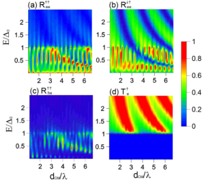
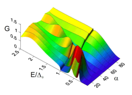
According to Eq. 15, in the range in which increases, the conductance is suppressed leading to the characteristics demonstrated in Fig. 13(a). In this figure the conductance suppression for the energy above corresponds to green areas. Nevertheless this suppression expands also on the subgap region for which is even grater than above [Fig. 14(b)]. The evolution of the conductance with increasing cone angle is presented in Fig. 15. We see that the conductance in the subgap region initially decreases and then clear conductance peak for appears. The position of this peak is shifted on the energy scale with increasing cone angle .
Finally, in Fig. 16 we present the conductance map calculated for and the exchange field amplitude . As shown in previous subsection in the non-adiabatic regime the decrease of results in decrease of the conductance in subgap region. This conductance suppression is different for different CM thicknesses (see Fig. 7) leading to the conductance peak for in consistency with the experimental results. Robinson et al. (2010)
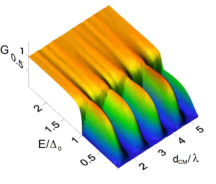
In the adiabatic regime the exchange field amplitude affects the conductance in a different manner. It leads to the conductance decay for the thicknesses being an integer multiples of whereas for the conductance remains almost unchanged. Therefore, the conductance in the sugap region oscillates regularly with the period as presented in Fig. 16.
IV Summary
We present the detailed analysis of the transport properties in the HM/CM/SC junction within the fully self-consistent framework based on the combined BTK formalism and the BdG equations. For comparison, the calculations have been also carried out with the use of the non-self consistent scheme. One has been shown that the peaks in the CM layer thickness dependence of the conductance are significantly reduced when the self-consistent procedure is applied (cf. Fig. 6). It is clear from our analysis that to properly determine the tunneling conductance in the HM/CM/SC heterojunctions the full self-consistent calculations including the proximity effect should be carried out.
Due to the spin band separation in the HM, the anomalous Andreev reflection mechanism which appears in structures with magnetically inhomogeneous layer (such as the CM layer) results in the nonzero conductance within the subgap region (cf. Fig. 3). Its probability strongly depends on the spin transmission in the CM layer. Therefore, we analyze the influence of the exchange field modulation on the behavior of spins of electrons transfered through the CM layer. With this respect, we show that one can distinguish between two regimes. In the non-adiabatic regime (low value of the exchange field modulation ) the changes of the exchange field are so fast that the spins of electrons are not able to adopt and, as a result, they rotate around irregularly and as an average give a small value of magnetization in comparison to the amplitude of the exchange field. On the other hand, in the adiabatic regime (high value of ) the magnetization coming from the spins of electrons is almost identical to the exchange field position dependence within the CM layer (cf. Fig 12). The conductance behavior as function of the energy and the CM layer thickness has different behavior in the two mentioned regimes (cf Figs. 5 and 13(c)). The regular oscillations observed in the adiabatic regime are caused by the fact that anomalous Andreev reflection probability is exactly proportional to the off-diagonal elements of the Hamiltonian . This leads to constant hight of the peaks in the CM layer thickness conductance dependence, whereas for the case of the non-adiabatic regime the hight of those peaks is decreasing with increasing thickness, , in consistency with the experiment observation (cf. Fig. 6). Moreover in the non-adiabatic regime the decrease of the exchange filed amplitude results in the well pronounced conductance peak for for which the peak of the critical current was observed in the experiment.Robinson et al. (2010) The influence of other parameters characterizing the exchange field behavior in the CM layer are also analyzed (such as the , and angles). It is shown that the conductance is strongly affected by the geometrical structure of the exchange field determined by the cone angle and the rotational a4.21a (PWD, AO, DPC) hacked
References
- Champel and Eschring (2005) T. Champel and M. Eschring, Phys. Rev. B 72, 054523 (2005).
- Braude and Nazarov (2007) V. Braude and V. Nazarov, Yu, Phys. Rev. Lett. 98, 077003 (2007).
- Houzet and Buzdin (2007) M. Houzet and I. A. Buzdin, Phys. Rev. B 76, 060504(R) (2007).
- L ofwander et al. (2007) T. L ofwander, T. Champel, J. Durst, and M. Eschring, Phys. Rev. Lett. 95, 187003 (2007).
- Buzdin (2005) A. I. Buzdin, Rev. Mod. Phys. 77, 035 (2005).
- Bergeret et al. (2005) F. S. Bergeret, A. F. Volkov, and K. B. Efetov, Rev. Mod. Phys. 77, 1321 (2005).
- Berezinskii (1974) V. L. Berezinskii, JETP Lett. 20, 287 (1974).
- Bergeret et al. (2001) F. S. Bergeret, A. F. Volkov, and K. B. Efetov, Phys. Rev. Lett. 86, 4096 (2001).
- Bergeret et al. (2003) F. S. Bergeret, A. F. Volkov, and K. B. Efetov, Phys. Rev. B 68, 064513 (2003).
- Volkov et al. (2003) A. F. Volkov, F. S. Bergeret, and K. B. Efetov, Phys. Rev. B 90, 117006 (2003).
- Andreev (1964) A. F. Andreev, JETP 19, 1228 (1964).
- Lambert and Raimondi (1998) C. J. Lambert and R. Raimondi, J. Phys. Condens. Matter 10, 901 (1998).
- Demler et al. (1997) E. A. Demler, G. B. Arnold, and M. R. Beasley, Phys. Rev. B 55, 15174 (1997).
- Fulde and Ferrell (1964) P. Fulde and A. Ferrell, Phys. Rev. 135, A550 (1964).
- Larkin and Ovchinnikov (1964) A. I. Larkin and Y. N. Ovchinnikov, Zh. Eksp. Teor. Fiz. 47, 1136 (1964).
- Fominov et al. (2005) Y. V. Fominov, A. F. Volkov, and K. B. Efetov, Phys. Rev. B 75, 104509 (2005).
- Lv. (2011) B. Lv., Eur. Phys. J. B 83, 493 (2011).
- Terrade et al. (2013) D. Terrade, P. Gentile, M. Cuoco, and D. Manske, Phys. Rev. B 88, 054516 (2013).
- Klose et al. (2012) C. Klose, T. S. Khaire, Y. Wang, W. P. Pratt jr., N. O. Birge, B. J. McMorran, T. P. Ginley, J. A. Borchers, B. J. Kirby, B. B. Maranville, and J. Unguris, Phys. Rev. Lett. 108, 127002 (2012).
- Gingrich et al. (2012) E. C. Gingrich, P. Quarterman, Y. Wang, R. Loloee, W. P. Pratt Jr., and N. O. Birge, Phys. Rev. B 86, 224506 (2012).
- Leksin et al. (2012) P. V. Leksin, N. N. Garif’yanov, I. A. Garifullin, Y. V. Fominov, J. Schumann, Y. Krupskaya, V. Katev, O. G. Schmidt, and B. Büchner, Phys. Rev. Lett. 109, 057005 (2012).
- Keizer et al. (2009) R. S. Keizer, S. T. B. Goennenwein, T. M. Klapwijk, G. Miao, G. Xiao, and A. Gupta, Nature (London) 439, 825 (2009).
- Khaire et al. (2010) T. S. Khaire, M. A. Khasawneh, W. P. Pratt Jr., and N. O. Birge, Phys. Rev. Lett. 104, 137002 (2010).
- Halterman and Valls (2005) K. Halterman and O. T. Valls, Phys. Rev. B 72, 060514(R) (2005).
- Halterman et al. (2007) K. Halterman, P. H. Barsic, and O. T. Valls, Phys. Rev. Lett. 99, 127002 (2007).
- Halterman et al. (2008) K. Halterman, O. T. Valls, and P. H. Barsic, Phys. Rev. B 77, 174511 (2008).
- Zhu et al. (2010) J. Zhu, I. N. Krivorotov, K. Halterman, and O. T. Valls, Phys. Rev. Lett. 105, 207002 (2010).
- Leksin et al. (2011) P. V. Leksin, N. N. Garifyanov, I. A. Garifullin, J. Schumann, V. Katev, O. G. Schmidt, and B. Büchner, Phys. Rev. Lett. 106, 067005 (2011).
- Wu et al. (2012a) C. T. Wu, O. T. Valls, and K. Halterman, Phys. Rev. B 86, 014523 (2012a).
- Robinson et al. (2010) J. W. A. Robinson, J. D. S. Witt, and M. G. Blamire, Science 329, 59 (2010).
- Alidoust and Linder (2010) M. Alidoust and J. Linder, Phys. Rev. B 82, 224504 (2010).
- Halász et al. (2011) G. Halász, M. G. Blamire, and J. W. A. Robinson, Phys. Rev. B 84, 024517 (2011).
- Wen et al. (2014) L. Wen, J. L. J, G. Q. Zha, and S. P. Zhou, 105, 27007 (2014).
- Jin et al. (2012) L. J. Jin, Y. Wang, L. Wen, and S. P. Zha, G Q nad Zhou, Physics Letters A 376, 2435 (2012).
- Wu et al. (2014) C.-T. Wu, O. T. Valls, and K. Halterman, Phys. Rev. B 90, 054523 (2014).
- Wu et al. (2012b) C.-T. Wu, O. T. Valls, and K. Halterman, Phys. Rev. B 86, 184517 (2012b).
- Wu et al. (2012c) C.-T. Wu, O. T. Valls, and K. Halterman, Phys. Rev. Lett. 108, 117005 (2012c).
- Blonder et al. (1982) G. E. Blonder, M. Tinkham, and T. M. Klapwijk, Phys. Rev. B 25, 4515 (1982).
- Bugoslavsky et al. (2005) Y. Bugoslavsky, Y. miyoshi, S. K. Clowes, W. R. Brandford, M. Lake, I. Brown, A. D. Caplin, and L. F. Cohen, Phys. Rev. B 71, 104523 (2005).
- Wójcik et al. (2011) P. Wójcik, A. Naylor, M. Wołoszyn, B. J. Hickey, B. J. Spisak, and J. Adamowski, J Supercond Nov Magn 24, 939 (2011).
- Groth et al. (2014) C. W. Groth, M. Wimmer, A. R. Akhmerov, and X. Waintal, New J. Phys. 16, 063065 (2014).
- Žutić and Valls (2000) I. Žutić and O. T. Valls, Phys. Rev. B 61, 1555 (2000).
ngle and .
Acknowledgments
This work was financed from the budget for Polish Science in the years 2013-2015. Project number: IP2012 048572.