Characteristics of Non-Irradiated and Irradiated Double SOI Integration Type Sensor
Mari ASANOA, Kazuhiko HARAA, Daisuke SEKIGAWAA, Shunsuke HONDAA, Naoshi TOBITAA, Yasuo ARAIB, Toshinobu MIYOSHIB, Ikuo KURACHIB
AUniversity of Tsukuba, Tsukuba, Ibaraki Japan.
BHigh Energy Accelerator Research Organization(KEK), Tsukuba, Ibaraki, Japan.
We are developing monolithic pixel sensors based on a 0.2 m fully-depleted Silicon-on-Insulator (SOI) technology for HEP experiment applications. The total ionizing dose (TID) effect is the major issue in the applications for hard radiation environments in HEP experiments. To compensate for TID damage, we have introduced a Double SOI structure which has a Middle Silicon layer (SOI2 layer) in addition. We studied the recovery from TID damage induced by ’s and other characteristics of an Integration-type Double SOI sensor. The Double SOI sensor irradiated to 100 kGy showed a response for IR laser similar to of a non-irradiated sensor when we applied a negative voltage to the SOI2 layer. We conclude that the Double SOI sensor is radiation hard enough to be used in HEP experiments in harsh radiation environments such as at Bell II or ILC.
PRESENTED AT
International Workshop on SOI Pixel Detector (SOIPIX2015), Tohoku University, Sendai, Japan, 3-6, June, 2015.
1 Introduction
1.1 SOI pixel sensor
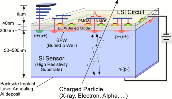
We are developing monolithic pixel sensors for various applications [1] based on a 0.2 m fully-depleted SOI technology. The schematics of an SOI pixel sensor is shown in Figure 1[2]. The sensors are processed by Lapis Semiconductor[3] on SOI wafers provided by SOITEC Co.[4]. For use in hard radiation environment as in HEP experiments, TID effect is the major issue[5].
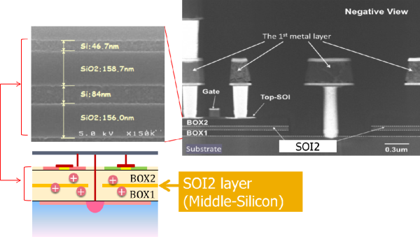
1.2 Double SOI
To compensate for TID damage, we introduced a Middle Silicon layer (SOI2 layer). By applying a negative voltage (), the effects due to irradiation-induced holes trapped in oxide layers are to be cancelled (Figure 2).
1.3 INTPIXh2
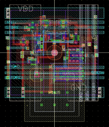
INTPIXh2 is an integration type SOI pixel sensor (see Table 1 for main parameters). Figure 4 is the on-pixel circuit of INTPIXh2. The pixel architecture is shown in Figure 5. The characteristics are compared between Double SOI and Single SOI types, which are fabricated in Double SOI wafer and Single SOI wafer, respectively. In the Double type, only the pixels in top-right sensor region (region-2) utilize the SOI2 layer (Figure 4). We used them to study the recovery from TID damage induced by ’s and to compare characteristics difference between Single SOI and Double SOI type sensors.
| INTPIXh2 parameters | |
|---|---|
| Pixel size | 18 m |
| Number of pixels | 280240 |
| Overall chip size | 6mm |
![[Uncaptioned image]](/html/1507.05382/assets/x3.png)
Only the pixels in Region-2 utilize the SOI2. ![[Uncaptioned image]](/html/1507.05382/assets/x4.png)
|
2 Response after 100 kGy irradiation
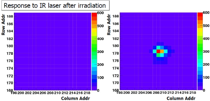
Response of a 100 kGy irradiated sensor (300 m thick, 100 V applied as reverse bias) to IR laser was clearly confirmed at while it was not at all at (see Figure 6). This demonstrates that applying a negative voltage to the SOI2 layer recovers the response of irradiated sensor to the level of non-irradiated one.
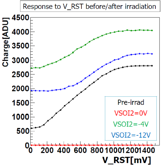
We studied the functionality of the circuit by measuring the output linearity w.r.t. the reset voltage amplitude ().
Figure 7 plots the results for the 100 kGy irradiated sensor (100 m thick, 100 V applied as reverse voltage), showing the recovery of the response by applying negative voltages to (green, blue). There was no response seen at (red). The response curve of a non-irradiated sensor is also plotted for comparison (black). The shifts in operation conditions, mainly thresholds, of the FETs induced by irradiation have not been completely recovered because a single common is applicable in this sensor design for various types of FETs employed. However, the response region has been clearly re-established by with the dynamic range being reduced partly.
.
3 Signal speed
We evaluated the signal time structure using a pulsed IR laser (wavelength 1064nm, signal width 50 ns, jitter 5 ns). Figure 9 shows the IR laser signal shape measured by a fast MPPC. We measured the output charge from INTPIXh2 as a function of delay time with a fixed integration time of 10 ns. By varying the delay time of integration start w.r.t. the IR laser trigger, we derived the information how fast the signal of INTPIXh2 is. The measured signal width is about 150 ns with a fast peaking time of 40 ns (Figure 9).
![[Uncaptioned image]](/html/1507.05382/assets/x8.png)
![[Uncaptioned image]](/html/1507.05382/assets/x9.png)
|
4 Cross talk
We measured the output signals from a pixel in which IR laser was injected and from the surrounding pixels (100 m thick n-bulk sensor). The laser spot size was set to 4 m square in order to inject the laser to one pixel only. We define the cross talk as the ratio of output signal height from a pixel to that from the pixel where laser was injected. The cross talk at low reverse bias voltage was substantial before irradiation (Figure10). However, the cross talk has decreased after irradiation. This is understood that the electrical isolation between pixels is improved by irradiation by accumulating electrons between p-type pixel nodes. The cross talk is found not to degrade by irradiation.
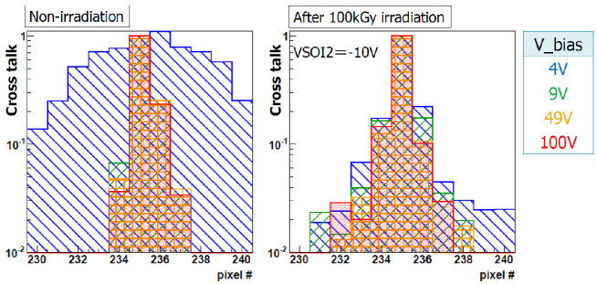
The collimated laser was spotted at pixel-235, and relative pulse heights in neighbouring pixels are plotted for typical bias voltages.
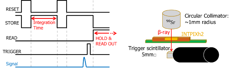
5 Response to MIP
The response to penetrating -rays was measured with INTPIXh2 Single and Double sensors. The -ray source was placed on top and penetrated was triggered by a plastic scintillator. The trigger system timing chart and geometry illustration are shown in Figure 11. Table 2 summarizes the parameters of INTPIXh2 set for the measurement. The -ray signal was reconstructed in a 55 pixel cluster with the seed centred at the pixel which has the maximum response in an event. Hit pixel distributions of the seeds in single-type and double-type sensors are shown in Figure 13 and Figure 15, respectively. The response of a single-type sensor showed a clear mip peak separated well from the pedestal with the peak value consistent with the calculation using a depletion thickness of 315 m (Figure 13). The response of a double-type sensor showed a mip peak with the peak as calculated using a 190 m thickness (Figure 15).
| INTPIXh2, single and double | |
|---|---|
| Integration Time | 1.00 s |
| 400 mV | |
| 150 V | |
![[Uncaptioned image]](/html/1507.05382/assets/x12.png)
![[Uncaptioned image]](/html/1507.05382/assets/x13.png)
|
![[Uncaptioned image]](/html/1507.05382/assets/x14.png)
![[Uncaptioned image]](/html/1507.05382/assets/x15.png)
|
6 Summary
We have introduced a double SOI structure for the purpose of compensating for TID damage. Characterization results obtained with non-irradiated and 100 kGy irradiated sensors conclude that the response from irradiated sensor is recoverable by applying negative voltage to the SOI2 layer. The double SOI sensor is radiation hard enough to be used in HEP experiments in hard radiation environment such as at Bell II or ILC.
ACKNOWLEDGEMENTS
The authors are grateful for fruitful collaboration with the Lapis Semiconductor Co. Ltd. The double SOI wafers have been realized through their excellence. This work was supported by JSPS KAKENHI Grand Number 25109006, by KEK Detector Technology Project and also by VLSI Design and Education Center (VDEC), The University of Tokyo, with the collaboration of the Cadence Corporation and Mentor Graphics Corporation.
References
- [1] T. Miyoshi et al., gMonolithic pixel detectors with 0.2 m FD-SOI pixel process technology, h Nucl. Instr. Meth. A732 (2013) 530.
- [2] SOIPIX collaboration group: http://rd.kek.jp/project/soi/.
- [3] Lapis Semiconductor Co., Ltd.: http://www.lapis-semi.com/en/.
- [4] SOITEC: http://www.soitec.com/en/technologies/smart-cut/.
- [5] S. Honda et al., g Total Ionization Damage Compensations in Double Silicon-on- Insulator Pixel Sensors h, Proceedings of Sciences (TIPP2014), 039, 2014.