Electronic transport in Si:P -doped wires
Abstract
Despite the importance of Si:P delta-doped wires for modern nanoelectronics, there are currently no computational models of electron transport in these devices. In this paper we present a nonequilibrium Green’s function model for electronic transport in a delta-doped wire, which is described by a tight-binding Hamiltonian matrix within a single-band effective-mass approximation. We use this transport model to calculate the current-voltage characteristics of a number of delta-doped wires, achieving good agreement with experiment. To motivate our transport model we have performed density-functional calculations for a variety of delta-doped wires, each with different donor configurations. These calculations also allow us to accurately define the electronic extent of a delta-doped wire, which we find to be at least 4.6 nm.
pacs:
73.22.-f, 73.63.-b, 73.63.NmI Introduction
Phosphorus doping in silicon with atomic precision has led to a variety of new nanostructures on the silicon platform Zwanenburg et al. (2013). Foremost among these are metallic wires that are “one atom tall and four atoms wide” Weber et al. (2012). These wires are made using a -doping technique that combines scanning-probe lithography with molecular-beam epitaxy Tucker and Shen (1998); O’Brien et al. (2001); Shen et al. (2002); Simmons et al. (2005). This technique achieves both high-density carrier concentrations and excellent two-dimensional (2D) confinement of phosphorus atoms in silicon McKibbin et al. (2010, 2014). For example, 2D doping densities of one in four inside a (001) silicon monolayer (i.e. 0.25 ML) have previously been reported Wilson et al. (2006). These high donor densities result in spatially confined electron transport when an in-plane voltage bias is applied to the nanostructure Rueß et al. (2008); Weber et al. (2014). Therefore, these systems have similar quantum mechanical properties to undoped silicon nanowires which are confined structurally Ko et al. (2001); Svizhenko et al. (2007); Ryu et al. (2015). The electronic properties of Si:P systems have applications for quantum computing and quantum communication technologies Kane (1998); Cole et al. (2005); Hollenberg et al. (2006). In this paper, we examine some of these properties for a phosphorus in silicon (Si:P) -doped wire Rueß et al. (2007a, b, 2008); Weber et al. (2012); McKibbin et al. (2013); Weber et al. (2014) using density-functional theory (DFT), effective-mass theory (EMT), the nonequilibrium Green’s function (NEGF) formalism, and tight-binding (TB) theory.
The long spin-coherence times and large Bohr radius of the phosphorus donor electron in silicon make this material an interesting candidate for spin-based devices and other nanoscale electronics Kohn and Luttinger (1955); Faulkner (1969); Tyryshkin et al. (2011); Steger et al. (2012). Si:P -doped wires might be used as the interconnects between stationary and flying qubits DiVincenzo (2000); Rueß et al. (2007a), low-resistivity source-drain contacts for nanoelectronics Clarke et al. (2008); Weber et al. (2012), or one-dimensional (1D) spin chains for confined magnon transport Balachandran and Gong (2008); Makin et al. (2012); Ahmed and Greentree (2015). The modern -doped wire is a quasi-1D row of phosphorus atoms oriented in the [110] crystallographic direction, with a width of 1.54 nm in the lateral [10] direction which is equivalent to two dimer rows (2DR) on the reconstructed (001) silicon surface Weber et al. (2012, 2014). In addition, because the placement of phosphorus atoms on the (001) plane is indeterministic Wilson et al. (2006); Schofield et al. (2006), a variety of donor configurations are possible within a realistic wire.
Computational models of Si:P -doped wires are limited to our density-functional model (Ref. Drumm et al., 2013a) and the empirical TB model of Ref. Ryu et al., 2013, where the nemo3d package is used to describe the equilibrium electronic properties of a Si:P -doped wire Weber et al. (2012). There are currently no computational models of electron transport in a -doped wire. However, electronic transport in an Si:P -doped layer has previously been investigated using a semi-classical model Hwang and Das Sarma (2013).
In this paper we calculate the electronic properties of a Si:P -doped wire for a variety of donor configurations. We investigate the effects of donor disorder and accurately define the electronic extent of a -doped wire. The current-voltage (I-V) characteristics of two -doped wires have recently been reported experimentally Weber et al. (2014). Therefore, we expand on our density-functional model by using it to develop the first computational model for electronic transport in a -doped wire. We calculate the I-V characteristics for the two -doped wires which have been reported experimentally and investigate the change in these characteristics for wires with larger in-plane widths. This computational model has wide applicability because it scales easily to large system sizes, which are needed to simulate realistic devices.
II Equilibrium electronic properties of -doped wires
In this section we present the results of our density-functional calculations for the equilibrium electronic properties of a variety of -doped wires. The equilibrium properties are those for which the potential difference between the source and drain contacts is equal to zero. Of particular interest are those properties relating to the spatial confinement or electronic extent of the donor electrons perpendicular to the axis of the wires. We make an important distinction between two closely related concepts: the electronic width and the electronic extent of the wires. The electronic width is defined as a measure of spread for the probability density of the donor electrons perpendicular to the wire axis (for example, the full-width half maximum of this probability distribution). This width is sometimes referred to as the “effective electronic diameter” of the wires Weber et al. (2012). The electronic extent of the wires is defined as the minimum distance of lateral separation at which two wires do not affect each other’s equilibrium electronic properties. Therefore, the electronic extent is the minimum distance at which two wires must be separated so they behave exactly as they do in isolation. By contrast, the electronic width is the region within which it is most likely to find the donor electrons.
II.1 Density-functional theory
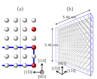
The siesta package was used to apply the Kohn-Sham self-consistent density-functional method in the generalized-gradient approximation Kohn and Sham (1965); Ordejón et al. (1996); Soler et al. (2002). This method was used to calculate the equilibrium electronic properties of the Si:P -doped wire shown in Fig. 1a. This wire is made of a single row of phosphorus atoms that have been doped into one dimer row (1DR) of the reconstructed (001) silicon surface and will therefore be referred to as the single-row wire. The single-row wire represents the 1D limit to scaling of the in-plane width of a phosphorus wire in silicon111At a 2D doping density of 0.25 ML.. A supercell for the single-row wire is shown in Fig. 1b where the axis of the wire is oriented in the direction. This supercell has dimensions of , which corresponds to at least 2.7 nm of bulk silicon “cladding” perpendicular to the wire axis222The supercell in Fig. 1b contains a total of 1120 atoms.. To avoid surface effects in the calculations, periodic boundary conditions are applied to the supercells. In Fig. 1, the periodic boundaries are shown as blue lines. The length of the supercell in the and directions is therefore determined by the amount of bulk silicon cladding that is needed to isolate the phosphorus wire from its periodic images.
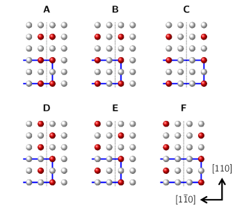
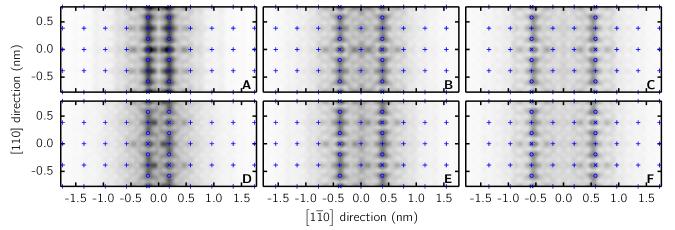
We have also performed density-functional calculations on the Si:P -doped wires shown in Fig. 2. These wires have been doped into two dimer rows (2DRs) of the reconstructed (001) silicon surfaceNote (1) and will be referred to as double-row wires A-F (see labels in Fig. 2). Double-row wires A-F represent all donor configurations which can result from adsorption of molecules onto a 2DR wide and 0.77 nm long region on the Si(001) surface, which is also periodic in the directionNote (1). For double-row wire B, we have previously found that by using 2.7 nm of bulk silicon cladding perpendicular to the wire axis, the minima of the occupied bands in the resulting band structure are converged to within 5 meV Drumm et al. (2013a).
To reduce the periodicity of the donor atoms in the direction we would need to at least double the length of the supercell in this directionNote (1). When the length of the supercell is doubled in one direction, the number of atoms in the supercell also doubles. This results in an impractical eightfold increase in the computation time of density-functional calculations. Therefore, the length of the supercells in the direction is limited to 0.77 nm for all wires considered herein. For double-row wires A-F, the lengths of the supercell in the and directions are the same as that for the supercell shown in Fig. 1b. However, the length of the supercell in the direction is larger so that there is always at least 2.7 nm of bulk silicon cladding perpendicular to the wires.
An optimized double- polarized basis set of localized atomic orbitals and norm-conserving Troullier-Martins pseudopotentials were used to variationally solve for the ground-state electron density of these -doped wires Budi et al. (2012); Troullier and Martins (1991). The lattice constant of bulk silicon was found to be 5.4575 Å using this basis set, which is in good agreement with the experimental value of 5.431 Å Becker et al. (1982). The exchange-correlation energy was calculated using the Perdew-Burke-Ernzerhof exchange-correlation functional Perdew et al. (1996). Total energies were converged to within using a Methfessel-Paxton occupation function of order 5 with an electronic smearing of 0.026 eV. The mesh energy grid cut-off used was 300 Ry. A Monkhorst-Pack -point grid was used to sample the Brillouin zone (BZ), which has previously been shown to give good results for double-row wire B Drumm et al. (2013a). The atomic positions of the silicon atoms were not geometrically optimized after phosphorus substitution because their positions are not significantly affected by this substitution Drumm et al. (2013b); Carter et al. (2009). Further details of our density-functional calculations are available in Refs. Budi et al., 2012; Drumm et al., 2013a, b.
II.2 Probability density of donor electrons
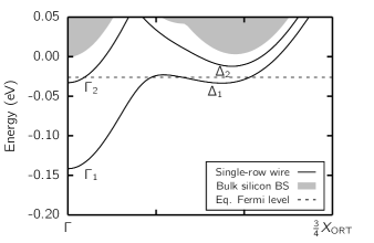
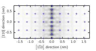
The probability density for the donor electrons in the single-row wire is shown in Fig. 3. This probability density has been calculated by integrating the local density of states (LDOS) between the conduction band (CB) edge and the equilibrium Fermi level of the single-row wire band structure shown in Fig. 4. Therefore, this probability density is a mixture of the states with minima , , and (which are labeled in Fig. 4). We can assume the donor electrons occupy the bands in this energy range because the valence band of bulk silicon is fully occupied at equilibrium and so the only bands that are available for the donor electrons are those of the CB. Experimental measurements of these systems are performed at and so we can also ignore the effects of electronic smearing (due to thermal motion) in this calculation Weber et al. (2012, 2014). The LDOS is calculated for the full supercell on a three-dimensional (3D) Cartesian grid, which is then line-averaged along the [001] direction (perpendicular to the donor plane) to make the probability density shown in Fig. 3. The probability distribution is normalized such that the integral of this probability density over the supercell is equal to the number of donor electrons inside the supercell. In Fig. 3, a distance equivalent to two supercells is shown in the [110] direction.
The donor electrons are partially delocalized along the axis of the phosphorus wire in Fig. 3. There is significant probability density not only on the phosphorus atoms but also the intervening silicon atoms both in- and out-of-plane. The majority of the probability density is localized to the atomic sites along the axis of the wire. Fig. 3 shows there is strong spatial confinement of the donor electrons perpendicular to the axis of the wire. The probability density decays sharply with distance from the wire axis in the direction. The majority of the probability density can seen to be localized to nm of the wire axis and, therefore, one may conclude that nm is a good approximation for the electronic extent of the wire. However, as we will demonstrate, this is not a valid approximation. Indeed, we will show that even nm is a poor approximation for the electronic extent of the single-row wire.
Fig. 5 shows the probability densities for double-row wires A-F. These probability densities have been calculated in the same way as Fig. 3. In each subfigure, there is significant overlap between the wavefunctions of the two rows of phosphorus atoms. The presence of this overlap is independent of whether the rows are staggered relative to one another or aligned (compare the probability densities of double-row wires A-C with those of double-row wires D-F). If the overlap between the two rows of phosphorus atoms is large enough such that they behave as a single wire, then the electronic width of this wire is strongly dependent on the donor configuration. The electronic width varies by as much as over double-row wires A-F and, therefore, we expect a similar variation in the width of a realistic wire.
Overall, it is difficult to determine the electronic extent of a -doped wire from these probability densities. Instead, we use the band structure of the wires and, in particular, energy splittings in the band minima to determine the electronic extent of a -doped wire.
II.3 Band structure of -doped wires
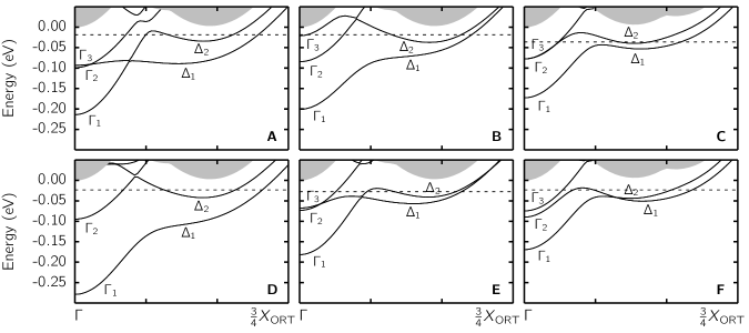
The band structure of bulk silicon calculated using a 1280-atom orthorhombic (ORT) supercell is shown as the gray shaded region in Fig. 4. There are two CB edges shown for bulk silicon, which are each doubly degenerate; one at and the other at , where in the -space direction. An explanation of the location of the bulk CB edges in this band structure is given in Appendix A. The band structure of the single-row wire is shown as solid lines in Fig. 4. The nuclear potential of the phosphorus atoms has moved the CB edges into the bulk bandgap region. The degeneracy of these CB edges or valleys has been broken, resulting in the appearance of four separate valleys. The minima of these four valleys are labeled as , , , and in Fig. 4.
It is well-known for -doped systems that an enhancement of the valley-orbit interaction due to spatial confinement will break the six-fold degeneracy of the bulk silicon CB edge, resulting in a valley splitting (VS) Carter et al. (2009, 2011); Drumm et al. (2012, 2013b). In Fig. 4, the 1D confinement caused by the donor potential has moved the CB edges into the bulk bandgap region and lifted their degeneracy by a VS. We report two different VSs for the single-row wire; one at labeled and another at labeled . The magnitude of the splitting is found to be 109 meV, which is within 10 meV of the same VS reported for -doped layers Drumm et al. (2013b). It has also been reported for -doped layers that CB valleys with higher curvature are moved further into the bulk bandgap region Drumm et al. (2012); Smith et al. (2014) and this is shown for the single-row wire in Fig. 4. In addition, we find the VS is larger for CB valleys with higher curvature. The magnitude of the splitting is found to be 21 meV, which is 19% of the splitting.
The position of the Fermi level shows three of the four CB valleys to be occupied at equilibrium; the , , and bands. The and minima at in the -space direction are symmetrically equivalent to two CB edges at . This is due to the symmetry of the path which is discussed in Appendix A. Therefore, for the single-row wire, we predict four conducting modes to be available for electron transport at low voltage biases.
The band structures for double-row wires A-F are shown in Fig. 6. The location of the bulk silicon CB edge for double-row wires C and F is at not , as discussed in Appendix A. For the double-row wires, the larger nuclear potential of more phosphorus atoms moves the CB valleys further into the bulk bandgap region compared to the single-row wire. The minima of these valleys are again labeled as , , , and . For all double-row wires (except double-row wire D) there is a third CB valley minimum at the point, labeled as in Fig. 6. The position of the Fermi level shows five CB valleys (including ) to be occupied at equilibrium for double-row wires A, C, E, and F. We expect there to be eight available conducting modes for the double-row wires, which is twice the number of available conducting modes as the single-row wire. However, there are only seven available conducting modes for double-row wires A, C, E, and F and six for double-row wires B and D when the symmetry of the path is taken into account.
The magnitudes of the and splittings are different for each of the double-row wires and, therefore, these VSs must be dependent on donor configuration. It has previously been reported for -doped layers that the magnitude of the splitting is dependent on the in-plane configuration of the donor atoms Carter et al. (2011). Fig. 6 shows the magnitude of the VS is affected by whether the two rows of phosphorus atoms are aligned (A, B, C) or staggered (D, E, F) relative to one another. The and splittings are largest for double-row wires A and D. These wires represent the donor configurations for which the two rows of phosphorus atoms are laterally separated by the smallest distance. The and splittings decrease as the distance of lateral separation increases in Fig. 6.
II.4 Electronic extent of a -doped wire in the one-dimensional limit
We expect there to be eight available conducting modes for double-row wires A-F. However, in the previous subsection, we report seven (and six) available conducting modes for double-row wires A, C, E, and F (and double-row wires B and D). Therefore, the number of available conducting modes in these wires is reduced by something so far unaccounted for. If there were zero overlap between the wavefunctions of each row of phosphorus atoms, the band structure for the double-row wires would be identical to the band structure of the single-row wire (except with each band being doubly degenerate). Therefore, we suggest is a degenerate pair of and that this degeneracy has been lifted by an energy splitting which is proportional to the wavefunction overlap between the two rows of phosphorus atoms333Given this hypothesis, we suggest the - splitting is not observed for double-row D because the splitting is so large that the minima cannot be distinguished from the higher energy modes of the silicon band structure.. We label this energy splitting as -. In Fig. 6, excluding double-row wires A and D, the - splitting decreases as the lateral separation of the two rows increases, i.e. as the wavefunction overlap between the two rows decreases so too does the - splitting. A similar energy splitting has previously been reported for two adjacent -doped layers Carter et al. (2013); Drumm et al. (2014).
In Fig. 7, the - splitting is plotted versus the lateral separation of the two rows of phosphorus atoms (between 0.8 nm and 4.6 nm). We also plot the - splitting versus the lateral separation of the two rows of phosphorus atoms in this figure. These energy splittings have been calculated by using supercells that are larger than those used for double-row wires A-F444The lengths of these supercells in the and directions are the same as that for double-row wires A-F. However, the length of the supercells in the direction is larger. In this direction, the length of the supercells is chosen such that there is always at least 2.7 nm of bulk silicon cladding surrounding the two rows of phosphorus atoms. Therefore, the maximum distance of lateral separation that can be investigated has to be less than 5.4 nm.. In Fig. 7, the - splitting tends towards the value of the VS calculated for the single-row wire as the lateral separation of the two rows is increased. By contrast, the - splitting tends towards zero as the lateral separation is increased. This suggests is a degenerate pair of and that the wavefunction overlap between the two rows of phosphorus atoms is what breaks this degeneracy.
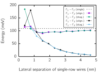
At a lateral separation of 1.9 nm, two additional CB valley minima appear at (when the two rows of phosphorus atoms are aligned), which we interpret as degenerate pairs of and that have also been lifted by an energy splitting. These splittings tend to zero as the lateral separation of the two rows is further increased. When the lateral separation is equal to 3.5 nm, a fourth CB valley minimum appears at which we suggest is the degenerate pair of . The energy splitting of the degeneracy is equal to 60 meV at a lateral separation of 3.5 nm and decreases to 37 meV by 4.6 nm, i.e. it has not converged to zero at a lateral separation of 4.6 nm.
We can now use this analysis of the splitting (and other energy splittings in , , and ) to approximate the electronic extent of the single-row wire. When the lateral separation of the two rows of phosphorus atoms is large, the two rows will each behave as single-row wires. The electronic extent of the single-row wire is then the lateral separation at which the energy splittings in , , , and are equal to zero. The - splitting and the energy splittings of the and degeneracies are approximately equal to 6 meV at a lateral separation of 4.6 nm. This is equal to the uncertainty in , , and . Therefore, to within the uncertainty of our density-functional method, the energy splittings in , and are indistinguishable from zero and so the electronic extent of the single-row wire is approximately equal to 4.6 nm. However, because the energy splitting in the degeneracy has not converged to zero by 4.6 nm, this is but a lower bound on the electronic extent of the single-row wire. Nonetheless, we expect this to be a good approximation because the occupancy of the state is much greater than that of the state, as shown in Fig. 4. For -doped wires that are separated by in-plane distances less than 4.6 nm, we predict a decrease in the number of available conducting modes at low voltage biases.
III Electronic transport properties of -doped wires
In this section we use the results of our density-functional calculations to construct a computational model of electron transport in a Si:P -doped wire. We solve for the electronic transport properties of a -doped wire using the general NEGF approach of Datta and others Datta (2006); Golizadeh-Mojarad and Datta (2007); Svizhenko et al. (2007); Ryndyk et al. (2009).
III.1 The nonequilibrium Green’s function formalism
The difficulty of solving for the eigenstates of a many-body system in the Schrödinger picture is avoided in the NEGF formalism by replacing the Hamiltonian operator by a Green’s function matrix. The transport properties of the system are then calculated from this Green’s function matrix. Our NEGF model describes a Si:P -doped wire using a TB Hamiltonian matrix, within a single-band effective-mass approximation, that is defined as
| (1) |
where is the on-site energy, is the tunneling parameter, and are first-nearest-neighbor donor atoms, and is the total number of donor atoms. is an offset to the on-site energy due to a gate voltage applied to the wire (with eV for a gate voltage equal to zero), is the dimension of the device, is the effective mass of the donor electrons (discussed below), and is the distance between two nearest-neighbor donor atoms.
A Si:P -doped wire is divided into three parts: a source, a drain, and a channel region that separates the two. In general, Eq. 1 describes the channel region only. However, in our NEGF model the source and drain contacts are described as semi-infinite extensions of the channel and, therefore, Eq. 1 is also used to describe the contacts. The retarded Green’s function matrix is then defined as
| (2) |
where is energy, is a positive infinitesimal real number, and and are the self-energy matrices for the source and drain respectively. These are given by
| (3) |
where is the coupling matrix between the contact and the channel, and is the surface Green’s function for the contact. We calculate the surface Green’s functions using the iterative scheme of Sancho et al., which solves the accompanying Dyson equation to arbitrary precision Sancho et al. (1985).
The transmission function for the device is written as
| (4) |
where is the degeneracy of the single band (discussed below), and and are the broadening matrices for the source and the drain respectively. These are given by
| (5) |
In the Landauer-Büttiker formalism, the current can then be calculated using the equation:
| (6) |
where is the elementary charge of an electron, is Planck’s constant and is the Fermi-Dirac distribution function for the contacts, defined as
| (7) |
In Eq. 7, is Boltzmann’s constant, is temperature (in Kelvin), and is the chemical potential of the source or drain which are given by
| (8) |
and
| (9) |
with the equilibrium chemical potential of the wire555The equilibrium chemical potential is measured relative to the energy of the CB edge when eV, which is not necessarily energy zero. and the source-drain bias voltage. For our calculations, the source-drain bias voltage decays linearly across the channel region.
The effective mass of the donor electrons is needed to fully specify the TB Hamiltonian in Eq. 2. This effective mass can be calculated for the single-row wire from the occupied CB valleys in the band struture shown in Fig. 4. The band dispersion in the neighborhood of the CB valley minima is approximately parabolic Drumm et al. (2012, 2013a). The curvature of this parabola is related to the effective mass of the donor electrons through the equation Drumm et al. (2013a):
| (10) |
Therefore, the effective mass of the donor electrons can be calculated by fitting parabola to the CB valleys in Fig. 4. However, it has previously been shown for double-row wire B that the curvature of these bands do not change significantly from their bulk values and so we may use the transverse and longitudinal effective masses of bulk silicon without modification Drumm et al. (2013a). In Fig. 4, the CB valleys at have high curvature; they are described by the transverse effective mass of bulk silicon Drumm et al. (2013a). The CB valleys at have low curvature; they are described by the longitudinal effective mass of bulk silicon Drumm et al. (2013a).
| (Å) | (K) | (eV) | |||
|---|---|---|---|---|---|
| 0.9163 666Ref. Hensel et al.,1965 | 7.718 | 4.2 777Ref. Weber et al.,2014 | 0.12 | 4 |
In Section II, it was shown for the single-row wire that there were four conducting modes available for electronic transport at low voltage biases. Therefore, we describe the single-row wire by one conducting mode that is four-fold degenerate within a single-band effective-mass approximation by setting in Eq. 4. We set the effective mass of this conducting mode equal to the average of the effective masses for the four occupied conducting modes. There are two occupied CB edges at and two occupied CB edges at . The average of the effective masses is given by
| (11) |
where there is a reduction of in the longitudinal effective mass (as discussed in Ref. Drumm et al., 2013a and Appendix A). The bulk silicon effective masses and , and the other parameters used in our NEGF model, are listed in Table 1. The equilibrium chemical potential is equal to the difference between and the equilibrium Fermi level for the single-row wire in Fig. 4. The atomic spacing is equal to the distance between two nearest-neighbor donor atoms in Fig. 1a. 2D wires with widths greater than that of the single-row wire are modeled as many adjacent single-row wires where the lateral separation of the donor atoms is equal to and the tunneling parameter for nearest-neighbor atoms in adjacent wires is equal to . Hardwall boundary conditions are applied in the dimension perpendicular to the axes of the wires.
III.2 I-V characteristics of -doped wires
In this section we present I-V characteristics for two -doped wires that have recently been measured in experiment Weber et al. (2014). One of the wires has a width of 4.6 nm, which is equivalent to 6 dimer rows (6DRs) on the reconstructed (001) silicon surface. The other wire has a width of 1.5 nm, which is equivalent to 2DRs on the same surface. In addition, we present I-V characteristics for wires that have widths larger than 4.6 nm. For means of comparison, all the wires have a channel region with a length of 47 nm (which is equal to the length spanned by the 6DR wire in experiment Weber et al. (2014)).
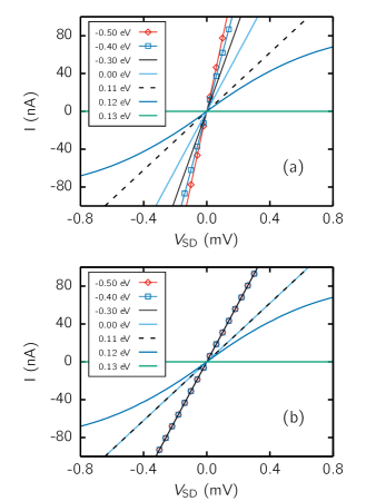
The I-V characteristics of the 6DR wire are shown in Fig. 8a. The I-V curve for eV shows a linear response when a non-zero source-drain bias voltage is applied to the 6DR wire. This linear response is characteristic of metallic conduction and is in good agreement with experimentWeber et al. (2014). The size of the current is approximately 2 times greater than in experiment when eV (see Fig. 1e of Ref. Weber et al., 2014).
In Fig. 8b, the I-V curve for eV shows a linear response when a bias voltage is applied to the 2DR wire. The size of the current is approximately 6 times greater than in experiment when eV (see Fig. 1f of Ref. Weber et al., 2014) and is exactly half that of the 6DR wire. Therefore, when eV there are double the number of available conducting modes in the 6DR wire than in the 2DR wire. The ratio of the two currents is also equal to two when eV as shown in Fig. 9a. The doubling in the number of available conducting modes is confirmed by the transmission functions for the two wires in Fig. 9b (compare the transmission function of the 6DR wire with that of the 2DR wire at in Fig. 9b).
The gradient of these I-V curves is equal to the differential conductance of the wires, which when divided by is equal to the number of conducting modes that are available for electron transport. To model the application of a gate voltage to the wires, we add a non-zero offset energy to the diagonal terms of the Hamiltonian matrix Graf and Vogl (1995) describing the channel region (see Eq. 1). An applied gate voltage will change the occupancy of the conducting modes in the wire and thereby change the conductance of the device.
Beginning with the I-V curve for eV in Fig. 8a, the differential conductance of the 6DR wire increases as is decreased to zero and then becomes increasingly negative. A negative offset energy in our NEGF model is equivalent to a positive gate voltage in experiment and, therefore, this trend is in good agreement with experiment Weber et al. (2014) (where the differential conductance increases as increasingly positive gate voltages are applied to the 6DR wire [see Fig. 1e of Ref. Weber et al., 2014]). A negative offset energy moves the unoccupied conducting modes to lower energies, making them available to conduction electrons and thereby increasing the conductance of the device. Alternatively, a positive offset energy moves the occupied conducting modes to higher energies, emptying these states of electrons and resulting in zero current because there are no longer any states available to conduction electrons (as shown in Fig. 8a for eV).
I-V curves for the 2DR wire are shown in Fig. 8b for the same offset energies that are applied to the 6DR wire in Fig. 8a. The relationship between these offset energies and the differential conductance of the 2DR wire is the same as that of the 6DR wire up to eV. Beyond this point, the differential conductance for the 2DR wire increases when eV and then remains constant as is made more negative (as shown for eV and eV). Therefore, when eV, the current in the 2DR wire has reached saturation because all of the conducting modes are occupied. By contrast, in the wider 6DR wire there remain conducting modes at higher energies that can be made available to conduction electrons by applying larger gate voltages.
Finally, in both Figs. 8a and 8b, there is a non-linear I-V response for eV (i.e. for ). When the offset energy is equal to the equilibrium chemical potential, the mean energy of the conduction electrons is equal to the energy of the CB edge. The application of a source-drain voltage bias broadens the energy of the conduction electrons but it also increases the energy of the CB edge. And, therefore, it is possible for the rate of change in the energy of the CB edge to be greater than the rate of change in the energy broadening of the conduction electrons. If this is the case then although the current will increase as the source-drain bias voltage is increased, the change in the current will decrease (as shown in Figs. 8a and 8b for eV). This non-linearity is not the same as the non-linear response reported experimentally for the 2DR wire (see Fig. 1f of Ref. Weber et al., 2014).
In general, there is good agreement between experiment and our results for the I-V characteristics of the 6DR wire. It is obvious that the results for the 6DR wire are in better agreement with experiment than the 2DR wire. This is the case for both the size of the current and the change in the current versus source-drain bias voltage. Therefore, we conclude that the 6DR wire is well-described by a ballistic model of electron transport, whereas the narrower 2DR wire is not. It is likely that a single-band effective-mass approximation is able to reproduce the low-temperature transport properties of the 6DR wire because the electron transport occurs at low voltage biases and, therefore, the higher energy modes of the silicon band structure are insignificant. This is promising for device simulation because our NEGF model scales easily to large system sizes.
There are a number of approximations in our NEGF model that could explain the discrepancies between theory and experiment. For the 6DR wire these include the value of the free parameters in Table 1, the boundary conditions, the average of the effective masses and the degeneracy of the single band in our effective-mass approximation. However, changing these properties will never reproduce the non-linear response reported experimentally for the 2DR wire Weber et al. (2014). To reproduce this non-linearity, we suggest it is necessary to extend our NEGF model to include donor disorder and non-ballistic transport. In this paper we have chosen to present the simplest model of electron transport in a Si:P -doped wire and, therefore, leave the investigation of these approximations to the subject of future work.
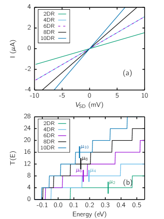
The transmission functions and equilibrium chemical potentials for wires with widths of 2DR, 4DR, 6DR, 8DR, and 10DR are shown in Fig. 9b. In this figure, is constant across all wires and is equal to -0.12 eV. The transmission functions and values of the equilibrium chemical potentials for each of these wires show that the number of available conducting modes increase as the width of the wires increase. Therefore, the I-V characteristics for the wider wires in Fig. 9a have larger differential conductances than the narrower wires. The energy of the lowest conducting modes decrease as the width of the wires increase, as shown in Fig. 9b. The spatial confinement of the donor electrons, perpendicular to the wire axis, decreases as the width of the -doped wire increases; thereby moving the conducting modes to lower energies in a similar fashion to the eigenenergies of an infinite potential well. This decrease in spatial confinement also decreases the energy splittings between the conducting modes, which is shown in Fig. 9b as a narrowing of the steps in the transmission functions. Finally, it should be noted that the width of the steps in the transmission functions are related to the splitting888As well as the other energy splittings in the , , and minima that were discussed in Section II, excluding the VSs.. Otherwise the transmission functions for the 2DR, 4DR, 6DR, 8DR, and 10DR wires would vary only by a multiplicative constant.
IV Conclusions
The band structure of a -doped wire has been calculated for a variety of donor configurations. We find a valley splitting at , in agreement with previous density-functional calculations of -doped layers. In addition, for -doped wires comprised of more than a single row of phosphorus atoms, we find another energy splitting at . This energy splitting () is not caused by the valley-orbit interaction but by wavefunction overlap between the adjacent rows of phosphorus atoms. The splitting is then used to calculate the electronic extent of the single-row wire, which is found to be at least 4.6 nm. When two single-row wires are separated by in-plane distances less than 4.6 nm, the resulting energy splittings reduce the number of available conducting modes and, therefore, conductance at low bias voltages.
Furthermore, we present a nonequilibrium Green’s function model for electron transport in a Si:P -doped wire. We calculate the I-V characteristics of a variety of -doped wires which have different in-plane widths, achieving good agreement with experiment. These wires show a linear response to an applied bias voltage, which is characteristic of the metallic conduction that is observed in experiment. We also show that the conductance can be controlled by applying a gate voltage to the wires. In the future this NEGF model could be extended to include donor disorder and non-ballistic transport.
Acknowledgements.
The authors acknowledge the support of the NCI National Facility (Canberra, Australia).Appendix A Band folding in -doped wires
We analyze the band structure of the -doped wires with respect to the band structure of bulk silicon. It is well-known that silicon is an indirect bandgap semiconductor with a sixfold degenerate CB edge Madelung (1996). These six CB edges are located at in the first BZ of the face-centered cubic (FCC) Bravais lattice, one along each of the six directions (where is the lattice constant of bulk silicon). The band structure of bulk silicon calculated using a 2-atom FCC unit cell is shown in Fig. 10, where is a point of high symmetry in the first BZ of the FCC unit cell and the path lies along one of the directions in reciprocal space Bradley and Cracknell (1972). The CB edges are located at in Fig. 10 as . The band dispersion in the neighborhood of the CB edges is approximately parabolic Drumm et al. (2012, 2013a) and, therefore, in reciprocal space these CB edges can be represented in 3D by spheroidal surfaces of constant energy centered at Singleton (2001) as shown in Fig. 11a. The spheroidal surfaces are anisotropic because the curvature of the band dispersion in silicon is anisotropic.
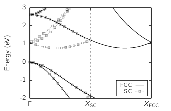
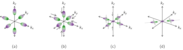
Fig. 10 also shows the band structure of bulk silicon calculated using an 8-atom simple cubic (SC) unit cell. From a comparison of the two band structures, we see the location of the CB edges and, therefore, spheroids in reciprocal space is dependent on the real-space unit cell that is used for the calculation, which is a result of band folding as discussed in our earlier work (see Appendices 1 and 2 of Ref. Drumm et al., 2013b). In Fig. 10, the BZ is folded about due to a doubling in the length of the supercell in the direction from 2.73 Å (for the FCC unit cell) to 5.46 Å (for the SC unit cell). When the length of the unit cell is increased in one dimension, the length of the BZ in the equivalent reciprocal dimension is decreased. The CB edges are thereby folded along their corresponding reciprocal space dimension towards the point999In general, when length of the BZ is decreased in one dimension, the distance between the CB edge and the point is not certain to decrease (this relationship is not monotonic). Rather, this distance decreases on average as the length of the BZ in this dimension is decreased. at . The CB edges have been folded from to in Fig. 10 and this is also shown in Fig. 11b by the translation of the spheroids along each of the cardinal axes towards .
The band structure of bulk silicon calculated using a 1280-atom orthorhombic (ORT) supercell (for example, see Fig. 1b) is shown as the gray shaded region in Fig. 4. There are two CB edges at energy zero; one at and the other at . These are each doubly degenerate and, therefore, represent four of the six CB edges of bulk silicon. The other two CB edges are located at and are not shown as they are symmetrically equivalent to those at . The locations of the CB edges in reciprocal space are dependent on the supercell that is used for the calculation and the resulting band folding of the SC (and ultimately FCC) band structure. Therefore, the location of the CB edges for the 1280-atom ORT supercell can be predicted from the band structure calculated using the 8-atom SC unit cell and simple geometric arguments.
To see how the SC band structure can be used to calculate the location of the CB edges for the 1280-atom ORT supercell, consider the simulation cell for an Si:P -doped layer. We use a 16-atom tetragonal (TET) unit cell to represent -doped layers because the phosphorus atoms are doped in-plane at densities of 0.25 ML and the supercell needs to include at least four silicon atoms in the donor plane (so one of these atoms can be substituted by a phosphorus atom for a doping density of one in four) Budi et al. (2012); Drumm et al. (2013b).
The TET unit cell is rotated by about the axis compared to the 8-atom SC unit cell. This rotation does not affect the location of the CB edges in reciprocal space, only their relative position in the first BZ of the TET unit cell. The length of the TET unit cell in the (i.e. ) direction is greater than that of the SC unit cell and this folds the CB edges in the direction towards . If the length of the TET unit cell in the direction is increased, it becomes a TET supercell. If this TET supercell is large enough to separate the -doped layer from its periodic images in the direction, then the CB edges in the direction are folded to the point101010The CB edges are only approximately folded to . This approximation is only exact in the limit as the length of the TET unit cell in the direction tends to infinity.. This folding is shown as a “flattening” of the spheroids to the plane in Fig. 11c. In this figure, there are CB edges located at and in the direction and, indeed, these have previously been reported for a TET supercell Drumm et al. (2013b).
The length of the simulation cell must also be large in the direction for an Si:P -doped wire so the 1D confinement of the donor electrons can be modeled accurately. In addition, the length of the simulation cell in the direction will be different to the length of the simulation cell in the direction (for atomistic simulations) because of the different crystallographic symmetries in each of these directions. Therefore, we must use an ORT supercell rather than a TET supercell to simulate the -doped wires.
The ORT supercell is elongated in the direction compared to the TET supercell, which shortens the equivalent reciprocal space dimension of the first BZ (parallel to the -space direction and perpendicular to the line ). The four CB edges at in Fig. 11c are thereby folded along the -space direction towards the line , as is shown in Fig. 11d. Two of the six CB edges are located at along the line in Fig. 11d and another two at along the same line. There is also a contraction of the valleys for these four CB edges as a result of this folding and, ultimately, the rotation of the ORT supercell (relative to the SC unit cell) Drumm et al. (2013a). This contraction of the valleys causes an effective doubling in the curvature of the band dispersion and, therefore, a reduction of in the corresponding effective mass Drumm et al. (2013a). In addition, the CB edges are only approximately folded onto the line . This approximation is only exact in the limit as the length of the ORT supercell in the direction tends to infinity. Therefore, the CB edge along the path in Figure 4 is located at rather than (where in the -space direction). For double-row wires C and F, where the length of the ORT supercell in the direction is larger, the same CB edge is located at in the -space direction111111For double-row wires C and F, the ORT supercell is elongated in the direction so that the amount of silicon cladding perpendicular to the phosphorus wires is not less than 2.7 nm..
References
- Zwanenburg et al. (2013) F. A. Zwanenburg, A. S. Dzurak, A. Morello, M. Y. Simmons, L. C. L. Hollenberg, G. Klimeck, S. Rogge, S. N. Coppersmith, and M. A. Eriksson, Reviews of Modern Physics 85, 961 (2013).
- Weber et al. (2012) B. Weber, S. Mahapatra, H. Ryu, S. Lee, A. Fuhrer, T. C. G. Reusch, D. L. Thompson, W. C. T. Lee, G. Klimeck, L. C. L. Hollenberg, and M. Y. Simmons, Science 335, 64 (2012).
- Tucker and Shen (1998) J. Tucker and T.-C. Shen, Solid-State Electronics 42, 1061 (1998).
- O’Brien et al. (2001) J. L. O’Brien, S. R. Schofield, M. Y. Simmons, R. G. Clark, A. S. Dzurak, N. J. Curson, B. E. Kane, N. S. McAlpine, M. E. Hawley, and G. W. Brown, Physical Review B 64, 161401 (2001).
- Shen et al. (2002) T.-C. Shen, J.-Y. Ji, M. A. Zudov, R.-R. Du, J. S. Kline, and J. R. Tucker, Applied Physics Letters 80, 1580 (2002).
- Simmons et al. (2005) M. Y. Simmons, F. J. Rueß, K. E. J. Goh, T. Hallam, S. R. Schofield, L. Oberbeck, N. J. Curson, A. R. Hamilton, M. J. Butcher, R. G. Clark, and T. C. G. Reusch, Molecular Simulation 31, 505 (2005).
- McKibbin et al. (2010) S. R. McKibbin, W. R. Clarke, and M. Y. Simmons, Physica E: Low-dimensional Systems and Nanostructures 42, 1180 (2010).
- McKibbin et al. (2014) S. R. McKibbin, C. M. Polley, G. Scappucci, J. G. Keizer, and M. Y. Simmons, Applied Physics Letters 104, 123502 (2014).
- Wilson et al. (2006) H. F. Wilson, O. Warschkow, N. A. Marks, N. J. Curson, S. R. Schofield, T. C. G. Reusch, M. W. Radny, P. V. Smith, D. R. McKenzie, and M. Y. Simmons, Physical Review B 74, 195310 (2006).
- Rueß et al. (2008) F. J. Rueß, A. P. Micolich, W. Pok, K. E. J. Goh, A. R. Hamilton, and M. Y. Simmons, Applied Physics Letters 92, 052101 (2008).
- Weber et al. (2014) B. Weber, H. Ryu, Y.-H. M. Tan, G. Klimeck, and M. Y. Simmons, Physical Review Letters 113, 246802 (2014).
- Ko et al. (2001) Y.-J. Ko, M. Shin, S. Lee, and K. W. Park, Journal of Applied Physics 89, 374 (2001).
- Svizhenko et al. (2007) A. Svizhenko, P. W. Leu, and K. Cho, Physical Review B 75, 125417 (2007).
- Ryu et al. (2015) H. Ryu, J. Kim, and K.-H. Hong, Nano Letters 15, 450 (2015).
- Kane (1998) B. E. Kane, Nature 393, 133 (1998).
- Cole et al. (2005) J. H. Cole, A. D. Greentree, C. J. Wellard, L. C. L. Hollenberg, and S. Prawer, Physical Review B 71, 115302 (2005).
- Hollenberg et al. (2006) L. C. L. Hollenberg, A. D. Greentree, A. G. Fowler, and C. J. Wellard, Physical Review B 74, 045311 (2006).
- Rueß et al. (2007a) F. J. Rueß, B. Weber, K. E. J. Goh, O. Klochan, A. R. Hamilton, and M. Y. Simmons, Physical Review B 76, 085403 (2007a).
- Rueß et al. (2007b) F. J. Rueß, K. E. J. Goh, M. J. Butcher, T. C. G. Reusch, L. Oberbeck, B. Weber, A. R. Hamilton, and M. Y. Simmons, Nanotechnology 18, 044023 (2007b).
- McKibbin et al. (2013) S. R. McKibbin, G. Scappucci, W. Pok, and M. Y. Simmons, Nanotechnology 24, 045303 (2013).
- Kohn and Luttinger (1955) W. Kohn and J. M. Luttinger, Physical Review 98, 915 (1955).
- Faulkner (1969) R. A. Faulkner, Physical Review 184, 713 (1969).
- Tyryshkin et al. (2011) A. M. Tyryshkin, S. Tojo, J. J. L. Morton, H. Riemann, N. V. Abrosimov, P. Becker, H.-J. Pohl, T. Schenkel, M. L. W. Thewalt, K. M. Itoh, and S. A. Lyon, Nature Materials 11, 143 (2011).
- Steger et al. (2012) M. Steger, K. Saeedi, M. L. W. Thewalt, J. J. L. Morton, H. Riemann, N. V. Abrosimov, P. Becker, and H.-J. Pohl, Science 336, 1280 (2012).
- DiVincenzo (2000) D. P. DiVincenzo, Fortschritte der Physik 48, 771 (2000).
- Clarke et al. (2008) W. R. Clarke, X. Zhou, A. Fuhrer, C. M. Polley, D. L. Thompson, T. C. G. Reusch, and M. Y. Simmons, Physica E: Low-dimensional Systems and Nanostructures 40, 2131 (2008).
- Balachandran and Gong (2008) V. Balachandran and J. Gong, Physical Review A 77, 012303 (2008).
- Makin et al. (2012) M. I. Makin, J. H. Cole, C. D. Hill, and A. D. Greentree, Physical Review Letters 108, 017207 (2012).
- Ahmed and Greentree (2015) M. H. Ahmed and A. D. Greentree, Physical Review A 91, 022306 (2015).
- Schofield et al. (2006) S. R. Schofield, N. J. Curson, O. Warschkow, N. A. Marks, H. F. Wilson, M. Y. Simmons, P. V. Smith, M. W. Radny, D. R. McKenzie, and R. G. Clark, The Journal of Physical Chemistry B 110, 3173 (2006).
- Drumm et al. (2013a) D. W. Drumm, J. S. Smith, M. C. Per, A. Budi, L. C. L. Hollenberg, and S. P. Russo, Physical Review Letters 110, 126802 (2013a).
- Ryu et al. (2013) H. Ryu, S. Lee, B. Weber, S. Mahapatra, L. C. L. Hollenberg, M. Y. Simmons, and G. Klimeck, Nanoscale 5, 8666 (2013).
- Hwang and Das Sarma (2013) E. H. Hwang and S. Das Sarma, Physical Review B 87, 125411 (2013).
- Kohn and Sham (1965) W. Kohn and L. J. Sham, Physical Review 140, A1133 (1965).
- Ordejón et al. (1996) P. Ordejón, E. Artacho, and J. M. Soler, Physical Review B 53, 10441R (1996).
- Soler et al. (2002) J. M. Soler, E. Artacho, J. D. Gale, A. García, J. Junquera, P. Ordejón, and D. Sánchez-Portal, Journal of Physics: Condensed Matter 14, 2745 (2002).
- Note (1) At a 2D doping density of 0.25 ML.
- Note (2) The supercell in Fig. 1b contains a total of 1120 atoms.
- Budi et al. (2012) A. Budi, D. W. Drumm, M. C. Per, A. Tregonning, S. P. Russo, and L. C. L. Hollenberg, Physical Review B 86, 165123 (2012).
- Troullier and Martins (1991) N. Troullier and J. L. Martins, Physical Review B 43, 8861 (1991).
- Becker et al. (1982) P. Becker, P. Scyfried, and H. Siegert, Zeitschrift für Physik B Condensed Matter 48, 17 (1982).
- Perdew et al. (1996) J. P. Perdew, K. Burke, and M. Ernzerhof, Physical Review Letters 77, 3865 (1996).
- Drumm et al. (2013b) D. W. Drumm, A. Budi, M. C. Per, S. P. Russo, and L. C. L Hollenberg, Nanoscale Research Letters 8, 111 (2013b).
- Carter et al. (2009) D. J. Carter, O. Warschkow, N. A. Marks, and D. R. McKenzie, Physical Review B 79, 033204 (2009).
- Carter et al. (2011) D. J. Carter, N. A. Marks, O. Warschkow, and D. R. McKenzie, Nanotechnology 22, 065701 (2011).
- Drumm et al. (2012) D. W. Drumm, L. C. L. Hollenberg, M. Y. Simmons, and M. Friesen, Physical Review B 85, 155419 (2012).
- Smith et al. (2014) J. S. Smith, J. H. Cole, and S. P. Russo, Physical Review B 89, 035306 (2014).
- Note (3) Given this hypothesis, we suggest the - splitting is not observed for double-row D because the splitting is so large that the minima cannot be distinguished from the higher energy modes of the silicon band structure.
- Carter et al. (2013) D. J. Carter, O. Warschkow, N. A. Marks, and D. R. McKenzie, Physical Review B 87, 045204 (2013).
- Drumm et al. (2014) D. W. Drumm, M. C. Per, A. Budi, L. C. L. Hollenberg, and S. P. Russo, Nanoscale Research Letters 9, 443 (2014).
- Note (4) The lengths of these supercells in the and directions are the same as that for double-row wires A-F. However, the length of the supercells in the direction is larger. In this direction, the length of the supercells is chosen such that there is always at least 2.7 nm of bulk silicon cladding surrounding the two rows of phosphorus atoms. Therefore, the maximum distance of lateral separation that can be investigated has to be less than 5.4 nm.
- Datta (2006) S. Datta, Quantum Transport: Atom to Transistor, 1st ed. (Cambridge University Press, Cambridge, 2006).
- Golizadeh-Mojarad and Datta (2007) R. Golizadeh-Mojarad and S. Datta, Physical Review B 75, 081301 (2007).
- Ryndyk et al. (2009) D. A. Ryndyk, R. Gutiérrez, B. Song, and G. Cuniberti (Springer Berlin Heidelberg, Berlin, Heidelberg, 2009) pp. 213–335.
- Sancho et al. (1985) M. P. L. Sancho, J. M. L. Sancho, J. M. L. Sancho, and J. Rubio, Journal of Physics F: Metal Physics 15, 851 (1985).
- Note (5) The equilibrium chemical potential is measured relative to the energy of the CB edge when eV, which is not necessarily energy zero.
- Hensel et al. (1965) J. C. Hensel, H. Hasegawa, and M. Nakayama, Physical Review 138, A225 (1965).
- Graf and Vogl (1995) M. Graf and P. Vogl, Physical Review B 51, 4940 (1995).
- Note (6) As well as the other energy splittings in the , , and minima that were discussed in Section II, excluding the VSs.
- Madelung (1996) O. Madelung, ed., Semiconductors - Basic Data, 2nd ed. (Springer, London, 1996).
- Bradley and Cracknell (1972) C. J. Bradley and A. P. Cracknell, The mathematical theory of symmetry in solids: Representation theory for point groups and space groups, 1st ed. (Oxford University Press, London, 1972).
- Singleton (2001) J. Singleton, Band Theory and Electronic Properties of Solids, 1st ed. (Oxford University Press, New York, 2001).
- Note (7) In general, when length of the BZ is decreased in one dimension, the distance between the CB edge and the point is not certain to decrease (this relationship is not monotonic). Rather, this distance decreases on average as the length of the BZ in this dimension is decreased.
- Note (8) The CB edges are only approximately folded to . This approximation is only exact in the limit as the length of the TET unit cell in the direction tends to infinity.
- Note (9) For double-row wires C and F, the ORT supercell is elongated in the direction so that the amount of silicon cladding perpendicular to the phosphorus wires is not less than 2.7 nm.