Charging of Cu atom on Mo supported thin films of ScN, MgO and NaF
Abstract
Molybdenum supported thin films of ScN, MgO and NaF with a Cu adatom have been studied in the framework of density functional theory. We have observed a charge transfer from the metal/film interface to the Cu atom and investigated its relation to surface and interface deformations. We find that a weak interaction between the metal and the film is a promising prerequisite for adatom charging. The detailed study of Cu/NaF/Mo and NaF/Mo indicates that the distortion of the NaF film caused by the Cu adsorption has essentially anharmonic character, as it is coupled to a strong charge redistribution in the system.
I Introduction
Modern experimental techniques made it possible to grow epitaxial films with atomic precision creating a whole new class of complex materials with unique properties where interfaces often play the decisive role Suntola (1992); Freund et al. (1996); Freund (2007); Freund and Pacchioni (2008); Honkala (2014). Ultrathin films of insulating materials grown on a metal support are one example of such materials Freund (2007); Freund and Pacchioni (2008); Honkala (2014); Wu et al. (1991); Franchy (2000); Chambers (2000). In particular, due to the proximity of the insulator/metal interface to the vacuum/insulator interface the adsorption properties of such complex substrates can be completely different from those of the surfaces of the corresponding insulating materials Freund (2007); Freund and Pacchioni (2008); Honkala (2014); Pacchioni et al. (2005); Giordano et al. (2005); Broqvist and Grönbeck (2006); Sterrer et al. (2007a); Honkala and Häkkinen (2007); Frondelius et al. (2008). This makes complex substrates very interesting for applications in the field of heterogeneous catalysis Freund (2007); Freund and Pacchioni (2008); Honkala (2014).
In this regard, one of the intriguing properties of metal supported thin films is a charging of neutral atoms adsorbed on them. This phenomenon was first found when the charge of an Au atom adsorbed on NaCl supported by Cu was manipulated with scanning tunneling microscope (STM) Repp et al. (2004). The gold atom was reversibly switched between the two states: stable \ceAu^0 and charged \ceAu^-. This experimental finding was also supported by density functional theory (DFT) calculations Repp et al. (2004).
A spontaneous adatom charging was for the first time predicted in DFT calculations for an Au atom deposited onto MgO/Mo Pacchioni et al. (2005). The gold atom on this substrate appeared to be negatively charged and its adsorption energy turned out to be significantly increased as compared to the adsorption of Au on MgO Pacchioni et al. (2005). These theoretical findings were later supported by experimental results Sterrer et al. (2007a). More recently the charging effect was intensively studied theoretically and experimentally for different combinations of metal support and thin film materials, and adsorbates (see, for example, Ref. Giordano et al., 2005, 2006; Giordano and Pacchioni, 2006; Grönbeck, 2006; Broqvist and Grönbeck, 2006; Honkala and Häkkinen, 2007; Giordano et al., 2007; Prada et al., 2008; Nilius et al., 2008; Hellman and Grönbeck, 2008; Frondelius et al., 2008; Giordano et al., 2008; Simic-Milosevic et al., 2008; Lin et al., 2009; Sicolo et al., 2009; Nilius et al., 2010; Martinez et al., 2010; Hellman et al., 2009; Ricci et al., 2006; Sterrer et al., 2007b; Frondelius et al., 2007; Nilius et al., 2012; Goniakowski et al., 2009; Goniakowski and Noguera, 2009).
Summarizing the current knowledge about metal supported thin films and their adsorption properties we notice the following facts. Thin films can substantially reduce the work function of support metals Giordano et al. (2005, 2006); Giordano and Pacchioni (2006); Prada et al. (2008), which should lead to easier charge transfer. However, the charging of adatoms can also happen despite the increase of work function Hellman and Grönbeck (2008). For charging adatom should have high enough electron affinity Pacchioni et al. (2005); Giordano et al. (2005).
The origin of adatom charge was found to be the metal and oxide interface as shown for Au/MgO/Ag Honkala and Häkkinen (2007), \ceNO2 /MgO /Ag Grönbeck (2006), \ceNO2 /BaO /Pt Broqvist and Grönbeck (2006), and \ceNO2 /Al2O3 /Ag Hellman and Grönbeck (2008). The electron abstraction from the interface modifies the oxide/metal interaction and increases the adhesion between film and metal Grönbeck (2006); Honkala and Häkkinen (2007). It was also established that the charging of adatom is a long-range phenomenon and could occur for relatively thick films Frondelius et al. (2008). Honkala et al. Honkala and Häkkinen, 2007 showed that the charge of Au on MgO/Mo was almost independent of the thickness of MgO ranging from 1 to 5 monolayers.
Although the formation of negatively charged species on metal supported ultrathin films is quite a widespread phenomenon, the mechanism behind the charging is still under debate. First, it was suggested to be a direct electron tunneling from the support metal conduction band states to the adatom empty states Pacchioni et al. (2005); Giordano et al. (2005); Giordano and Pacchioni (2006); Martinez et al. (2010). However, many authors avoid this concept (see, e.g. Refs. Broqvist and Grönbeck, 2006; Honkala and Häkkinen, 2007; Frondelius et al., 2008; Pacchioni, 2014; Goniakowski et al., 2009), emphasizing instead the role of electrostatic interaction and system polarization Broqvist and Grönbeck (2006); Honkala and Häkkinen (2007); Frondelius et al. (2008); Goniakowski et al. (2009). We also notice that charge redistribution at metal/insulator interfaces was intensively studied in semiconductor physics Schottky (1938, 1939); Mott (1938, 1939) and a number of useful concepts, such as band bending and space charge layer formation were developed Schottky (1938, 1939); Mott (1938, 1939); Zhang and Yates (2012).
It is known that charging is accompanied by surface distortions around the adsorbed adatom Pacchioni et al. (2005); Giordano et al. (2005). Moreover, calculations show that there is no charging on “frozen” surfaces Giordano et al. (2007); Frondelius et al. (2008). The importance of rumpling and surface distortion was most consistently studied by Goniakowski et al. (Refs. Goniakowski et al., 2009; Goniakowski and Noguera, 2009), who showed that the charge transfer from the metal into the thin film or adatom is quasilinearly proportional to the rumpling of the interface. Moreover, these works reported an important finding that the relationship between the charge transfer and film deformation were similar for both bare supported films and the films with adatoms Goniakowski et al. (2009); Goniakowski and Noguera (2009). Their results suggest that interface rumpling is a response of the system to the spontaneous charge redistribution at the interface Goniakowski et al. (2009); Goniakowski and Noguera (2009).
Here we report the results of a systematic study of the ScN/Mo, MgO/Mo and NaF/Mo systems with a Cu adatom. MgO, ScN and NaF were chosen for their simple rock-salt structure and small lattice mismatch with Mo. The anions of these compounds are neighbours in the Periodic Table of elements that can yield a trend in properties. Moreover, NaF and MgO are ionic compounds, while ScN is more covalent and is a semiconductor, which allows us to do a comparative study. The questions we focus on are why and when charging takes place, how it happens, which atoms and electronic states are involved in the charging process.
This article is organized as follows. Section II describes methodology and computational details. Section III contains results and discussions. In Section III.1 and III.2 we describe systems AB/Mo and Cu/AB/Mo (AB = ScN, MgO, NaF), respectively, in particular, factors enhancing charging as well as connection between the charge transfer and deformation of the film induced by adsorption. In Section III.3 we investigate the origin of the adatom charge and where it accumulates. Next, in Section III.4 we demonstrate how the charge is “pumped” from film/metal interface to the top surface layer, and show which electronic states are involved. In Section IV we summarize our findings and provide concluding remarks.
II Methodology and computational details
II.1 Model Description
The ultrathin films of three binary compounds on the surface of bcc molybdenum (AB/Mo, AB = ScN, MgO, NaF) both bare and with an adsorbed Cu atom (Cu/AB/Mo) have been studied. Such epitaxially grown thin films usually adopt rocksalt structure Smith et al. (2001); Benedetti et al. (2008), which we consider here. Thus, an AB/Mo interface is constructed of the AB (001) surface and Mo (001) surface, rotated by with respect to each other. The anion atoms (B = N, O, F) are located directly above the Mo atoms, while the cation atoms (A = Sc, Mg, Na) are above the hollow sites of the Mo lattice. The calculations were carried out for the symmetric slabs, having two AB monolayers (ML) on both sides of a 9 ML thick molybdenum slab (Fig. 1). The thickness of the Mo slab was chosen based on the convergence of the following characteristics i) distances between adjacent (001) Mo planes, ii) density of states (DOS) of surface Mo layer, iii) surface energy. Also, the middle layer of the slab should possess bulk-like properties. Our tests show that to have a good representation of the mentioned properties one can use 9 ML thick Mo slabs. The repeated slabs were separated by at least 17 Å of vacuum.
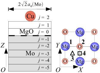
Since the films are ultrathin, while the metal support is supposed to be bulk-like Benedetti et al. (2008) we matched the lattice parameters of the films to the one of Mo and aligned them with ( factor appears due to the Mo(001) surface rotation by ). The lattice mismatch parameters ( and are lattice constants of the film and support) for ScN, MgO and NaF on Mo are , and , respectively (as calculated from the experimental lattice constants Refs. Pawar, 1967; Lengauer, 1988; Tsirelson et al., 1998; Deshpande, 1961). Plus sign here means that the film is compressed with respect to the bulk lattice parameter, while minus means the film is expanded. The lattice mismatch is modest and the most strained film, MgO/Mo, has successfully been synthesized (see, e.g. Ref. Wu et al., 1991; Benedetti et al., 2008).
For all the surfaces we considered four sites for Cu adsorption: 1) on top of cation, 2) on top of anion, 3) hollow site above the center of the square comprised of two cations and two anions, and 4) bridging position above the center of the cation and anion bond (Fig. 1). The Cu atom at these sites was allowed to relax along the axis.
II.2 Computational Details
Density functional theory (DFT) calculations were performed using the projector augmented wave method Blöchl (1994) together with the general gradient approximation (GGA) in Perdew-Budke-Ernzernhof parametrization Perdew et al. (1996, 1997) as implemented in Vienna Ab initio Simulation Package Kresse and Hafner (1993, 1994); Kresse and Furthmüller (1996, 1996); Kresse and Joubert (1999). The cutoff energy of 800 eV was used in the calculations. The following states were included into the valence band: Cu , Sc , N , Mg , O , Na , F , and Mo . The Brillouin zone was sampled over a Pack-Monkhorst -points mesh Monkhorst and Pack (1976). The calculations were spin polarized. During geometry optimization the relaxation of all atoms except for the Mo atoms in the middle symmetry layer (, see Fig. 1) was allowed. A geometry was considered to be optimized if forces acting on unfrozen atoms were less than 5 meV/Å.
We notice that even though standard GGA functionals underestimate band gaps, they adequately describe charging phenomena in metal supported thin films that has been demonstrated by numerous previous works Pacchioni et al. (2005); Giordano et al. (2005); Broqvist and Grönbeck (2006); Sterrer et al. (2007a); Honkala and Häkkinen (2007); Frondelius et al. (2008); Giordano and Pacchioni (2006); Grönbeck (2006); Broqvist and Grönbeck (2006); Honkala and Häkkinen (2007); Giordano et al. (2007); Nilius et al. (2008); Hellman and Grönbeck (2008); Frondelius et al. (2008); Simic-Milosevic et al. (2008); Lin et al. (2009); Sicolo et al. (2009); Nilius et al. (2010); Martinez et al. (2010); Hellman et al. (2009); Ricci et al. (2006); Sterrer et al. (2007b); Frondelius et al. (2007); Hellman et al. (2009). Moreover, it has recently been shown that both standard GGA and hybrid functional produce very similar Bader charges of an Au adatom on MgO and CaO substrates doped with Mo or Cr Prada et al. (2013).
To understand the mechanism of adatom charging on the AB/Mo surfaces we analysed the atomic charges calculated using the Bader approach Bader (1990); Tang et al. (2009). We also found it elucidative to analyze the sum of atomic charges in separate layers (an approach also used in Ref. Goniakowski and Noguera, 2004). In order to choose an optimal grid we tested the convergence of Bader charges with respect to the grid density. Our tests showed that the Bader charge of a monolayer was much more sensitive to the grid step in the direction than in the other directions that allowed us to save computational resources by choosing a non-uniform grid with smaller steps along the axis. The step values: and resulted in the Bader charges with the accuracy of about per monolayer and about per atom.
III Results and Discussions
III.1 ScN/Mo, MgO/Mo, NaF/Mo
First, we calculated the bulk and surface properties of the involved materials. The calculated lattice constant of bcc Mo, , is in good agreement with the experimental value of Pawar (1967), and the calculated surface energy of Mo(001), (), is close to experimental () Che et al. (1998). The calculated work function of Mo(001), , is underestimated compared to the experimental value of 4.53 eV Berge et al. (1974). The underestimation of the work function by GGA for similar systems is well-known Giordano et al. (2005). The calculated lattice constants of bulk ScN, MgO and NaF are 4.500 Å (4.501 Å Lengauer (1988)), 4.240 Å (4.214 Å Tsirelson et al. (1998)), 4.705 Å (4.634 Å Deshpande (1961)), respectively (experimental values are given in parentheses). Notice that in the calculations of the complex substrates reported here the Mo lattice parameter was used. The calculated band gap values for ScN, MgO and NaF are 0.1 eV (1.3 eV Gall et al. (2001)), 4.6 eV (7.7 eV Madelung (2004)) and 6.1 eV (11.5 eV Roy et al. (1985)), respectively (experimental values are given in parentheses). As expected the band gap values are underestimated.
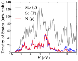
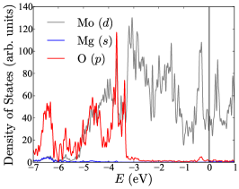
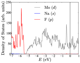
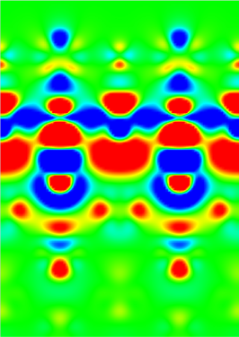
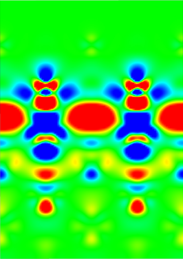
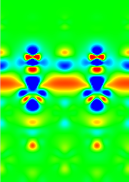
The electronic structure, charge density redistribution pattern and other calculated characteristics of the metal supported thin films are shown in Figs. 2, 3 and Table 1. The densities of states demonstrate that the states of ScN and Mo are strongly mixed, the states of MgO and Mo are moderately mixed, while for those of NaF and Mo virtually there is no mixing (Fig. 2). The calculated adhesion energy follows this trend decreasing from ScN to NaF. The interface distance, on the contrary, increases from ScN to NaF (Table 1), indicating a somewhat stronger bonding between ScN and Mo compared to the other considered cases. The charge density difference maps (Fig. 3) show a noticeable charge redistribution at the ScN/Mo interface involving even the second layer of ScN. In the case of MgO/Mo the charge redistribution at the interface is less pronounced with mostly O atoms being affected. In the case of NaF/Mo the redistribution is quite weak. Rumpling at the interface is more pronounced for MgO/Mo and NaF/Mo, than for ScN/Mo. The reduction of the work function is least pronounced for ScN/Mo and most pronounced for NaF/Mo.
| ScN/MO | MgO/Mo | NaF/Mo | |
|---|---|---|---|
| 0.204 | 0.130 | 0.039 | |
| (eV) | 3.14 | 1.85 | 1.28 |
| 2.11 | 2.15 | 2.41 | |
| 0.02 | 0.04 | 0.02 | |
| 0.02 | 0.08 | 0.04 |
Thus, our results demonstrate that the strength of Mo and film bonding decreases in the row: ScN, MgO, and NaF (Fig. 2, Fig. 3, and Table 1). Among the considered compounds ScN is the least ionic and NaF is the most ionic, which is also shown by the analysis of the Bader charges of the bulk compounds: , , and . Thus we observe the following trend: for more ionic films we find weaker adhesion to the metal, smaller overlap of the densities of states of the metal and the film, and less pronounced charge redistribution at the interface. As we show further, the strength of the interface bonding is also related to the charging of an adatom on the AB/Mo surface.
III.2 Cu Atom Adsorption on Mo Supported Thin Films
Spontaneous adatom charging is studied here by considering the adsorption of Cu atom on the AB/Mo surfaces. Before going into details, we want to outline that the capability to negatively charge the Cu adatom increases in the sequence ScN/Mo, MgO/Mo, NaF/Mo — the same sequence in which the bonding strength, adhesion energy, intensity of charge redistribution and the work function of the AB/Mo substrate decrease.
In order to characterize the adsorption of Cu we investigated four adsorption sites: on top of cation, on top of anion, hollow and bridging, and calculated several quantities, such as, adsorption energy , Bader charge of Cu adatom , the vertical distance from Cu to the top layer (average position of atoms) , and rumpling of atomic layers , calculated from average coordinates of A and B in the layer with an index (see Fig. 1). The obtained results are summarized in Table 2.
| ScN/Mo | |||||
|---|---|---|---|---|---|
| Sc on-top | |||||
| N on-top | |||||
| N on-top* | |||||
| hollow | |||||
| MgO/Mo | |||||
| Mg on-top | |||||
| O on-top | |||||
| hollow | |||||
| hollow* | |||||
| bridging | |||||
| NaF-Mo | |||||
| Na on-top | |||||
| F on-top | |||||
| F on-top* | |||||
| hollow | |||||
| bridging |
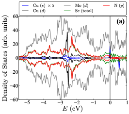
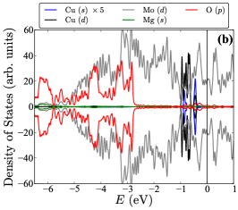
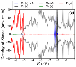
As one can see charging of Cu is most pronounced on NaF/Mo. For all the considered adsorption positions, the Cu states fall below the Fermi level and no spin-polarization is observed (see the example of F on-top site, Fig. 4c). The Bader charge of Cu is almost the same for all the positions, , which is in agreement with charges reported for similar systems, e.g. Au on MgO/Mo Honkala and Häkkinen (2007). Interestingly, despite fluorine being the most electronegative element of the Periodic Table Cu charging occurs even for Cu adsorbed on-top of F, which was found to be the most favorable adsorption site.
Charging of Cu on NaF/Mo is accompanied by substantial atomic displacements in the top NaF layer that results in rather large adsorption energies (from 1.651 to 1.877 eV). In particular, the F atom, situated below adsorbed Cu, moves downwards by 0.27 Å, while the four nearest Na atoms move upwards by 0.57 Å. A similar distortion pattern was reported for Au/MgO/Mo Pacchioni et al. (2005). Together with distortions around Cu we also observe a prominent average rumpling () of the NaF surface layer (, see Fig. 1) for all the adsorption sites (see Table 2). The significant changes occur also at the interface, where the inversion of rumpling is observed and becomes smaller than . Thus upon Cu adsorption on-top of F the Mo-F distance on average shortens by , as compared to that in NaF/Mo. For all the adsorption sites on NaF/Mo the same inversion of rumpling occurs (see Table 2). Similar structural changes were also reported for the \ceNO2 adsorption on \ceAl2O3 /Ag Hellman and Grönbeck (2008).
The characteristics of Cu adsorption on MgO/Mo are similar to those of Cu/NaF/Mo. Cu charging occurs for all the four adsorption sites. The Bader charges of Cu, , are smaller than those for Cu on NaF/Mo, but still significant ranging from to . The adsorption energies are rather large (from 1.326 eV to 1.466 eV), the favored adsorption site is the hollow site. The Cu adsorption on MgO/Mo is accompanied by notable surface relaxation. The two Mg atoms, nearest to Cu adsorbed at the hollow site, shift upwards by 0.19 Å, while two nearest O atoms move downwards by 0.11 Å. The average rumpling of the surface monolayer () is about . At the same time, rumpling of the interface MgO layer () is negligible as compared to that in the Cu/NaF/Mo system. The average vertical distances from O () to the Mo () layer and from Mg () to the Mo () layer are the same, 2.15 Å. Due to the Cu adsorption the Mo-O distance shortens by .
According to Bader analysis the Cu atom on MgO/Mo has a smaller charge than that on NaF/Mo, however, in both cases the Cu states are filled and no spin-polarization is observed (Fig. 4). Although the Bader analysis cannot be expected to unambiguously assign charges to atoms in a solid somewhat smaller charge of Cu on MgO/Mo corresponds to a smaller adsorption energy and smaller displacements of surface atoms in comparison with those for NaF/Mo.
On ScN/Mo, Cu prefers to adsorb on top of N that yields no charging. The Cu states are half occupied and mixed with the N states (Fig. 4a). Adsorption at this site results in Cu-N covalent bonding with the Cu-N distance of 1.86 Å and the adsorption energy of 1.609 eV. Surface relaxation in this case is very weak in comparison with all the cases where charging is observed.
As a matter of fact, charging of Cu occurs also on ScN/Mo for two adsorption sites: Sc on-top and hollow. However, even in these cases it is less pronounced than in the Cu/MgO/Mo and Cu/NaF/Mo systems. For Cu adsorbed at the Sc on-top site the Cu states are fully occupied (not shown) and at the hollow site Cu states are preponderantly occupied (not shown). The calculated Bader charges are still notable, and for the Sc on-top and hollow sites, respectively. The interface and surface rumpling is also negative as in the case of Cu/NaF/Mo but somewhat less pronounced (see Table 2).
We notice that as Cu gets charged at all adsorption sites on both MgO/Mo and NaF/Mo the resulting adsorption energies are quite similar that provides a flat energy profile for Cu on these surfaces, especially on MgO/Mo, and, therefore, simplifies surface diffusion. This is not the case for ScN/Mo where the adsorption energies are very different, e.g. 0.752 eV and 1.609 eV for the Sc on-top and N on-top positions, respectively.
It is well-known that without metal support adatom charging is negligible (see, e.g. Ref. Pacchioni et al., 2005; Amft and Skorodumova, 2010). We have examined Cu adsorption on top of anions in the Cu/AB systems (2ML AB with the same lattice parameter as in the other calculations). For the N on-top site of Cu/ScN we got = 1.523 eV and . For the O on-top site of Cu/MgO we got = 1.110 eV and . For the F on-top site of Cu/NaF we got = 0.380 eV and . Thus, in all these cases charging is negligible.
The comparison of Cu on ScN/Mo, MgO/Mo and NaF/Mo allows us to make some general conclusions regarding the capability of metal supported thin films to charge adatoms. As follows from our results this capability is enhanced from ScN/Mo to MgO/Mo and further to NaF/Mo. ScN is a covalent compound also forming covalent-like bonds with Mo, while MgO and NaF are ionic (see Section III.1). Therefore, to construct a system where a substantial charge transfer is possible one could use ionic films whose states are weakly mixed with those of the metal support. Strong adatom-substrate bonds can also prohibit the charge transfer whereas a weaker interaction between the adatom and a film can promote it. Notice that Cu and MgO (NaF) states almost do not mix. The same trend we find for Cu adsorbed at the Sc on-top and hollow sites on ScN/Mo where a charge transfer takes place. Thus, a minimum mixing between adatom and thin film states as well as between those of the insulating film and the metal support appear to be crucial for charging to occur.
We also investigated the adsorption of Cu on frozen surfaces for the most stable positions: N on-top site for Cu/ScN/Mo, hollow site for Cu/MgO/Mo, and F on-top site for Cu/NaF/Mo (see Table 2). For the F on-top (Cu/NaF/Mo) and hollow sites (Cu/MgO/Mo) the adsorption energies and Bader charges of Cu are reduced significantly. According to the density of states calculated for these cases the Cu spin-down states are split from the spin-up states and are not fully occupied. These findings agree with the results reported for the Au adsorption on frozen MgO/Ag Giordano et al. (2007); Frondelius et al. (2008). We also notice that in the case of Cu adsorption at the N on-top site of ScN/Mo the adsorption energy, Bader charge and the Cu-N distance calculated for the frozen and fully relaxed surfaces are very similar (see Table 2). This is due to the absence of charging in both cases, when the Cu-N bond is a dominating contribution to the adsorption energy. Also we observe, that if there is no charging or it is significantly reduced (as on frozen surfaces) the vertical distance from the Cu to the surface is shorter, while charged Cu shifts further away from the surface (see Table 2).
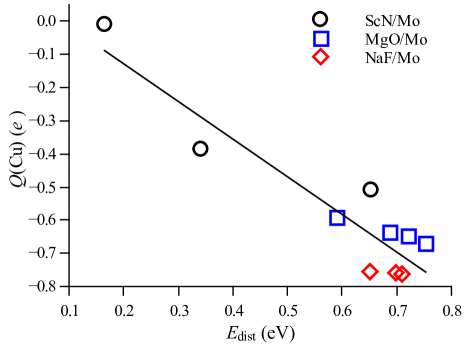
Thus our results confirm the importance of surface relaxation for adatom charging. We also find it useful to study the characteristics of the AB/Mo systems having exactly the same surface distortion as the Cu/AB/Mo systems (i.e. when all A, B and Mo atoms are kept in the same positions as in Cu/AB/Mo, but Cu is removed). We denote such systems by [Cu]/AB/Mo. The energy needed to distort the [Cu]/AB/Mo surface is then . could be used as a measure of surface distortion. In Fig. 5 we show the charge of Cu in Cu/AB/Mo versus distortion energy of [Cu]/AB/Mo, . There is a clear correlation between the energy of distortion and charge transferred to Cu, in fact, and charge are linearly proportional to each other.
III.3 Distortion Induced Charge Localization on AB/Mo surface
The charge accumulated by the Cu adatom comes from AB/Mo, but where is the origin of this charge? The analysis of the Bader charges of the substrate monolayers, calculated as described in Section II.2, makes it possible to answer this question. Here we study the charge distribution in Cu/AB/Mo, [Cu]/AB/Mo and AB/Mo. In Fig. 6 we show the layer charges for the three most stable configurations: N on-top site for Cu/ScN/Mo, hollow site for Cu/MgO/Mo and F on-top site for Cu/NaF/Mo.
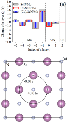
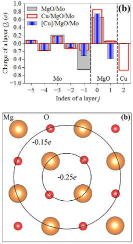
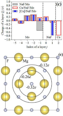
Let us, first, compare Cu/AB/Mo and AB/Mo. Fig. 6 (top panels) shows that for all Cu/AB/Mo the charge redistribution mostly occurs at the interface, while deeper Mo layers remain practically unaffected. For Cu adsorbed at the N on-top site, neither significant changes at the interface can be seen. For Cu adsorbed at the hollow site on MgO/Mo, where a significant charge transfer to Cu takes place, the charge of the adatom originates from the metal/oxide interface, mostly from the first Mo layer (Fig. 6b top panel). These findings for Cu/MgO/Mo and Cu/NaF/Mo agree well with previous reports on Au/MgO/Mo and \ceNO2/MgO/Mo Frondelius et al. (2008).
Let us now consider distorted [Cu]/AB/Mo, which has the geometry of relaxed Cu/AB/Mo but without Cu. In terms of charge redistribution not much difference between Cu/ScN/Mo and [Cu]/ScN/Mo is observed (see Fig. 6a). For [Cu]/MgO/Mo and [Cu]/NaF/Mo, however, one can see a strong polarization of AB and Mo as a result of the distortion. Similar to Cu/MgO/Mo and Cu/NaF/Mo, the charge is accumulated in the top surface monolayer of MgO and NaF (see Fig. 6). The amount of charge accumulated in the surface layer is for MgO and for NaF. The origin of the charge is again the MgO/Mo (NaF/Mo) interface (see Fig. 6).
The Bader analysis of atomic charges shows that the excess charge, which for a particular atom we define as , is spread over several atoms in the top layer (Fig. 6, bottom panels). In [Cu]/MgO/Mo most of the excess charge is accumulated in the surface layer around the hollow site and in the next coordination sphere. In [Cu]/NaF/Mo excess charge is localized at the F atom (below the Cu in Cu/NaF/Mo) and is localized at the four surrounding Na atoms. Thus, for both [Cu]/MgO/Mo and [Cu]/NaF/Mo the excess charge appears to be spread over the distorted top layer and its larger part is located at the adsorption site. The amount of this excess charge accumulated in the distorted AB top layer is almost equal to the charge of Cu in the corresponding Cu/AB/Mo system. Thus, in both cases with and without Cu, the distortion leads to similar charge redistribution. For more details on charge redistribution see Fig. 8 in Appendix A.
III.4 Charge Transfer From Metal Support to Adatom Through Thin Film: Cu/NaF/Mo case
In this section we discuss the role of the thin film distortion in the charge transfer to the Cu adatom using the case of Cu adsorbed at the F on-top site on NaF/Mo (Cu/NaF/Mo), where charging is most pronounced.
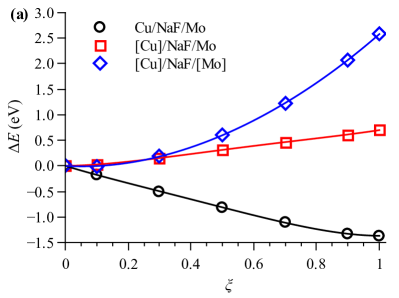
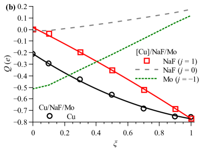
To see how charge redistribution depends on the degree of deformation we approximated the deformation path of the surface with a linear geometry transformation. Let us denote the set of coordinates of all the Na and F atoms in NaF/Mo with and those in Cu/NaF/Mo with , and introduce . Next, let us consider the linear path of geometry transformation from to , which is given by , where . For every value of the positions of Na and F atoms are defined and frozen, while Cu is allowed to relax.
Furthermore, we have considered the same linear transformation of NaF/Mo in the absence of Cu (the [Cu]/NaF/Mo case), as well as that of the NaF film in the absence of both Cu and Mo (the [Cu]/NaF/[Mo] case). Results are shown in Fig. 7.
It is clear that in the case of Cu adsorption on NaF/Mo (Cu/NaF/Mo) the relaxation occurs spontaneously without any barrier. The charge of adatom increases almost linearly along the deformation path. Bader analysis shows that for both Cu/NaF/Mo and [Cu]/NaF/Mo the charges of NaF (, see Fig. 1) and Mo () interface layers monotonically decrease along the path (shown for [Cu]/NaF/Mo, see Fig. 7b), thus charge is depleted from the NaF/Mo interface.
For Cu/NaF/Mo the gradually applied distortion yields gradual charging of Cu, while in the case of [Cu]/NaF/Mo it provides monotonic charge accumulation in the NaF top layer () (see Fig. 7b). Moreover, we notice that along the path the values of the charge of Cu in Cu/NaF/Mo and the charge of NaF () top layer in [Cu]/NaF/Mo are similar and become almost equal for .
Furthermore, our results indicate that the Na and F states participate in the charge transfer from the NaF/Mo interface to the Cu adatom (see Fig. 9 in Appendix B).
Our calculations show that charging requires distortion, i.e. cannot happen immediately (see Fig. 7). There are indications that metal supported ultrathin films have different phonon structure compared to thick films and should be more flexible Nelin et al. (2011). Indeed, energy changes shown in Fig. 7a demonstrate that it is much easier to deform [Cu]/NaF/Mo than [Cu]/NaF/[Mo]. The same distortion from to costs 0.70 eV for [Cu]/NaF/Mo and 2.58 eV for [Cu]/NaF/[Mo]. Moreover, the analysis of the curves show rather harmonic behavior for [Cu]/NaF/[Mo], while for [Cu]/NaF/Mo and Cu/NaF/Mo it is strongly anharmonic (see Fig. 7a). Notice that with (or without) Cu adatom the energy change is almost linearly proportional to the accumulated charge. Hence, we attribute the NaF/Mo anharmonicity to the coupling of deformation with the charge transfer from the Mo/NaF interface to the NaF top layer (in [Cu]/NaF/Mo) or Cu adatom (in Cu/NaF/Mo).
IV Conclusions
We have performed a systematic study of the AB/Mo and Cu/AB/Mo systems (AB = ScN, MgO, NaF). An enhancement of Cu adatom charging from ScN to MgO, and further to NaF is observed. The results suggest that charging is more pronounced when mixing between the states of the insulating film and metal substrate as well as between those of an adatom and thin film is small.
The film/metal interface is the origin of adatom charge. The charge transfer is accompanied with a strong surface relaxation around the adatom and structural changes at the film/metal interface. Our results on Cu/AB/Mo show clear correlation between the amount of transferred charge and the degree of system distortion. Moreover, the results of the constrained deformation calculations indicate that distortion is decisive for the charge transfer and it will “pump” the charge into the top surface layer irrespective of an adatom presence or absence on the surface.
We have found that the deformation of NaF/Mo film is essentially anharmonic, which we attribute to the coupling with the charge “pumping” from metal/film interface to the film/vacuum interface or adatom. Also, it is much easier to distort NaF/Mo than NaF, therefore we expect that softening of some phonon modes of the metal supported films takes place.
V Acknowledgements
We would like to acknowledge Swedish Research Council (VR) and Swedish Energy Agency (STEM) for the support. We also thank the Swedish National Infrastructure for Computing (SNIC) for provided computational resources. P.A.Ž. acknowledges A. V. Ruban for interesting discussions. P.A.Ž. also acknowledges VESTA Momma and Izumi (2011) software developers.
Appendix A Appendix A: Spatial Charge Distribution
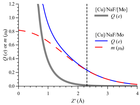
The spatial distribution of charge accumulated in [Cu]/NaF/Mo was examined further. In Fig. 8 we show charge density for [Cu]/NaF/Mo and [Cu]/NaF/[Mo] integrated along the axis. Let us recall, that [Cu]/NaF/Mo (also [Cu]/NaF/[Mo]) have the same geometry as Cu/NaF/Mo, but Cu (respectively Cu and Mo) are absent. One can see that in the [Cu]/NaF/Mo case charge is more spread in the direction compared to the case when both Cu adatom and Mo support are removed ([Cu]/NaF/[Mo]). In particular, for [Cu]/NaF/Mo approximately are found above the position of Cu in Cu/AB/Mo (note, there is no Cu in [Cu]/NaF/Mo). The same conclusion follows from the integrated magnetization curve, which agrees well with the integrated charge curve (Fig. 8).
Appendix B Appendix B: DOS of Na and F during deformation
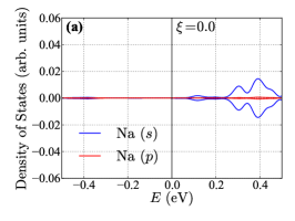
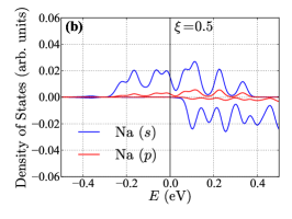
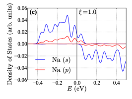
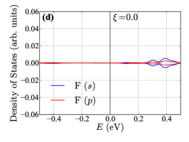
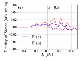
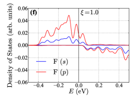
Here we report the details behind the distortion of [Cu]/NaF/Mo from to (see the main text for explanations). In Fig. 9 we show the evolution of the density of states near the Fermi level for [Cu]/NaF/Mo, namely, for the F atom underneath Cu in Cu/NaF/Mo and the nearest Na atoms in the top NaF layer. According to the Bader analysis these atoms accumulate the charge, while Mo atoms in the interface layer lose it (not shown) that agrees well with the evolution of the density of states. The number of the F states below the Fermi level (mainly the states) and Na states (mainly the states) gradually increases along the deformation path (see Fig. 9), while the number of the Mo states decreases (not shown). As a result of the charge transfer the system becomes spin polarized, near the Fermi level the spin-down states are unoccupied (see Fig. 9). Therefore, our findings indicate that the F and Na states participate in the charge transfer to Cu adatom.
References
- Suntola (1992) T. Suntola, Thin Solid Films 216, 84 (1992).
- Freund et al. (1996) H.-J. Freund, H. Kuhlenbeck, and V. Staemmler, Rep. Prog. Phys. 59, 283 (1996).
- Freund (2007) H.-J. Freund, Surf. Sci. 601, 1438 (2007).
- Freund and Pacchioni (2008) H.-J. Freund and G. Pacchioni, Chem. Soc. Rev. 37, 2224 (2008).
- Honkala (2014) K. Honkala, Surf. Sci. Rep. 69, 366 (2014).
- Wu et al. (1991) M.-C. Wu, J. S. Corneille, C. A. Estrada, J.-W. He, and D. W. Goodman, Chem. Phys. Lett. 182, 472 (1991).
- Franchy (2000) R. Franchy, Surf. Sci. Rep. 38, 195 (2000).
- Chambers (2000) S. A. Chambers, Surf. Sci. Rep. 39, 105 (2000).
- Pacchioni et al. (2005) G. Pacchioni, L. Giordano, and M. Baistrocchi, Phys. Rev. Lett. 94, 226104 (2005).
- Giordano et al. (2005) L. Giordano, M. Baistrocchi, and G. Pacchioni, Phys. Rev. B 72, 115403 (2005).
- Broqvist and Grönbeck (2006) P. Broqvist and H. Grönbeck, Surf. Sci. 600, L214 (2006).
- Sterrer et al. (2007a) M. Sterrer, T. Risse, U. M. Pozzoni, L. Giordano, M. Heyde, H.-P. Rust, G. Pacchioni, and H.-J. Freund, Phys. Rev. Lett. 98, 096107 (2007a).
- Honkala and Häkkinen (2007) K. Honkala and H. Häkkinen, J. Phys. Chem. C 111, 4319 (2007).
- Frondelius et al. (2008) P. Frondelius, A. Hellman, K. Honkala, H. Häkkinen, and H. Grönbeck, Phys. Rev. B 78, 085426 (2008).
- Repp et al. (2004) J. Repp, G. Meyer, F. E. Olsson, and M. Persson, Science 305, 493 (2004).
- Giordano et al. (2006) L. Giordano, F. Cinquini, and G. Pacchioni, Phys. Rev. B 73, 045414 (2006).
- Giordano and Pacchioni (2006) L. Giordano and G. Pacchioni, Phys. Chem. Chem. Phys. 8, 3335 (2006).
- Grönbeck (2006) H. Grönbeck, J. Phys. Chem. B 110, 11977 (2006).
- Giordano et al. (2007) L. Giordano, U. Martinez, S. Sicolo, and G. Pacchioni, J. Chem. Phys. 127, 144713 (2007).
- Prada et al. (2008) S. Prada, U. Martinez, and G. Pacchioni, Phys. Rev. B 78, 235423 (2008).
- Nilius et al. (2008) N. Nilius, M. V. Ganduglia-Pirovano, V. Brázdová, M. Kulawik, J. Sauer, and H.-J. Freund, Phys. Rev. Lett. 100, 096802 (2008).
- Hellman and Grönbeck (2008) A. Hellman and H. Grönbeck, Phys. Rev. Lett. 100, 116801 (2008).
- Giordano et al. (2008) L. Giordano, G. Pacchioni, J. Goniakowski, N. Nilius, E. D. L. Rienks, and H.-J. Freund, Phys. Rev. Lett. 101, 026102 (2008).
- Simic-Milosevic et al. (2008) V. Simic-Milosevic, M. Heyde, X. Lin, T. König, H.-P. Rust, M. Sterrer, T. Risse, N. Nilius, H.-J. Freund, L. Giordano, and G. Pacchioni, Phys. Rev. B 78, 235429 (2008).
- Lin et al. (2009) X. Lin, N. Nilius, H.-J. Freund, M. Walter, P. Frondelius, K. Honkala, and H. Häkkinen, Phys. Rev. Lett. 102, 206801 (2009).
- Sicolo et al. (2009) S. Sicolo, L. Giordano, and G. Pacchioni, J. Phys. Chem. C 113, 16694 (2009).
- Nilius et al. (2010) N. Nilius, M. V. Ganduglia-Pirovano, V. Brázdová, M. Kulawik, J. Sauer, and H.-J. Freund, Phys. Rev. B 81, 045422 (2010).
- Martinez et al. (2010) U. Martinez, L. Giordano, and G. Pacchioni, ChemPhysChem 11, 412 (2010).
- Hellman et al. (2009) A. Hellman, S. Klacar, and H. Grönbeck, J. Am. Chem. Soc. 131, 16636 (2009).
- Ricci et al. (2006) D. Ricci, A. Bongiorno, G. Pacchioni, and U. Landman, Phys. Rev. Lett. 97, 036106 (2006).
- Sterrer et al. (2007b) M. Sterrer, T. Risse, M. Heyde, H.-P. Rust, and H.-J. Freund, Phys. Rev. Lett. 98, 206103 (2007b).
- Frondelius et al. (2007) P. Frondelius, H. Häkkinen, and K. Honkala, New J. Phys. 9, 339 (2007).
- Nilius et al. (2012) N. Nilius, S. Benedetti, Y. Pan, P. Myrach, C. Noguera, L. Giordano, and J. Goniakowski, Phys. Rev. B 86, 205410 (2012).
- Goniakowski et al. (2009) J. Goniakowski, C. Noguera, L. Giordano, and G. Pacchioni, Phys. Rev. B 80, 125403 (2009).
- Goniakowski and Noguera (2009) J. Goniakowski and C. Noguera, Phys. Rev. B 79, 155433 (2009).
- Pacchioni (2014) G. Pacchioni, Chem. Rec. 14, 910 (2014).
- Schottky (1938) W. Schottky, Die Naturwissenschaften 26, 843 (1938).
- Schottky (1939) W. Schottky, Zeitschrift für Physik 113, 367 (1939).
- Mott (1938) N. Mott, Proc. Cambridge Philos. Soc. 34, 568 (1938).
- Mott (1939) N. Mott, Proc. R. Soc. London, Ser. A 171 (1939).
- Zhang and Yates (2012) Z. Zhang and J. T. Yates, Chemical Reviews 112, 5520 (2012), pMID: 22783915, http://dx.doi.org/10.1021/cr3000626 .
- Smith et al. (2001) A. R. Smith, H. A. H. AL-Brithen, D. C. Ingram, and D. Gall, J. Appl. Phys. 90, 1809 (2001).
- Benedetti et al. (2008) S. Benedetti, P. Torelli, S. Valeri, H. M. Benia, N. Nilius, and G. Renaud, Phys. Rev. B 78, 195411 (2008).
- Pawar (1967) R. R. Pawar, Curr. Sci. India 36, 428 (1967).
- Lengauer (1988) W. Lengauer, J. Solid State Chem. 76, 412 (1988).
- Tsirelson et al. (1998) V. G. Tsirelson, A. S. Avilov, Y. A. Abramov, E. L. Belokoneva, R. Kitaneh, and D. Feil, Acta Crystallogr. B 54, 8 (1998).
- Deshpande (1961) V. T. Deshpande, Acta Crystallogr. 14, 794 (1961).
- Blöchl (1994) P. E. Blöchl, Phys. Rev. B 50, 17953 (1994).
- Perdew et al. (1996) J. P. Perdew, K. Burke, and M. Ernzerhof, Phys. Rev. Lett. 77, 3865 (1996).
- Perdew et al. (1997) J. P. Perdew, K. Burke, and M. Ernzerhof, Phys. Rev. Lett. 78, 1396 (1997).
- Kresse and Hafner (1993) G. Kresse and J. Hafner, Phys. Rev. B 47, 558 (1993).
- Kresse and Hafner (1994) G. Kresse and J. Hafner, Phys. Rev. B 49, 14251 (1994).
- Kresse and Furthmüller (1996) G. Kresse and J. Furthmüller, Comp. Mater. Sci. 6, 15 (1996).
- Kresse and Furthmüller (1996) G. Kresse and J. Furthmüller, Phys. Rev. B 54, 11169 (1996).
- Kresse and Joubert (1999) G. Kresse and D. Joubert, Phys. Rev. B 59, 1758 (1999).
- Monkhorst and Pack (1976) H. Monkhorst and J. Pack, Phys. Rev. B 13, 5188 (1976).
- Prada et al. (2013) S. Prada, L. Giordano, and G. Pacchioni, J. Phys. Chem. C 117, 9943 (2013).
- Bader (1990) R. Bader, Atoms in Molecules: A Quantum Theory, International series of monographs on chemistry (Clarendon Press, 1990).
- Tang et al. (2009) W. Tang, E. Sanville, and G. Henkelman, J. Phys. Condens. Mat. 21, 084204 (2009).
- Goniakowski and Noguera (2004) J. Goniakowski and C. Noguera, Interface Sci. 12, 93 (2004).
- Che et al. (1998) J. G. Che, C. T. Chan, W.-E. Jian, and T. C. Leung, Phys. Rev. B 57, 1875 (1998).
- Berge et al. (1974) S. Berge, P. Gartland, and B. Slagsvold, Surf. Sci. 43, 275 (1974).
- Gall et al. (2001) D. Gall, M. Städele, K. Järrendahl, I. Petrov, P. Desjardins, R. T. Haasch, T.-Y. Lee, and J. E. Greene, Phys. Rev. B 63, 125119 (2001).
- Madelung (2004) O. Madelung, Semiconductors: Data Handbook (Springer-Verlag Berlin Heidelberg, 2004).
- Roy et al. (1985) G. Roy, G. Singh, and T. Gallon, Surf. Sci. 152-153, Part 2, 1042 (1985).
- Amft and Skorodumova (2010) M. Amft and N. V. Skorodumova, Phys. Rev. B 81, 195443 (2010).
- Nelin et al. (2011) C. J. Nelin, P. S. Bagus, M. A. Brown, M. Sterrer, and H.-J. Freund, Angew. Chem. Int. Edit. 50, 10174 (2011).
- Momma and Izumi (2011) K. Momma and F. Izumi, J. Appl. Crystallogr. 44, 1272 (2011).