Quantum transport properties in Datta-Das tuned opacity spin-transistors
Abstract
We studied the spin-dependent quantum transport properties using a simple modelling of a Datta-Das spin transistor. We refine previous results by accounting the propagation medium changes of opacity felt by itinerant electrons, when the gate-voltage is switched on and modelling them via the transversal energy levels mismatch. Monitoring the topological-dependent conductance, we are able to identify the device operating points. If the incoming electrons energy approaches the biased-induced barriers height, the spin-resolved conductance oscillations become significant. In a zero temperature picture, our computations of the spin-dependent conductance as function of the electric field at the region below the gate electrode suggest the feasibility of the modeled device. Although we demonstrate that phase time may not be spin-resolved, our simulation allows us to evaluate the time that takes an electron to experience a spin-flip process, resulting in an order of magnitude lower than typical values of the spin relaxation times.
pacs:
71.70.Ej, 85.75.Hh, 03.65.Xp, 85.75.-dI Introduction
One of the biggest challenges in Spintronics Awschalom and Flatté (2007); Chen and Buyanova (2014) is to achieve an efficient manipulation of the spin degree of freedom at zero magnetic field. Rashba spin-orbit coupling (SOC-R) Bychkov and Rashba (1984a, b) is among the most promising phenomena. SOC-R is a natural consequence of an asymmetry in the confining potential of carriers in low dimensional semiconductor systems, so-called structure inversion asymmetry (SIA) Winkler . To intuitively understand SOC-R some authors consider that electrons feel a potential gradient due to SIA, which Lorentz transforms into an effective magnetic field that acts over theirs spin. Nonetheless, attention most be paid since Lorentz transformation neglects the atomic cores contribution to SOC-R, felts by a Bloch electron in a solid Winkler .
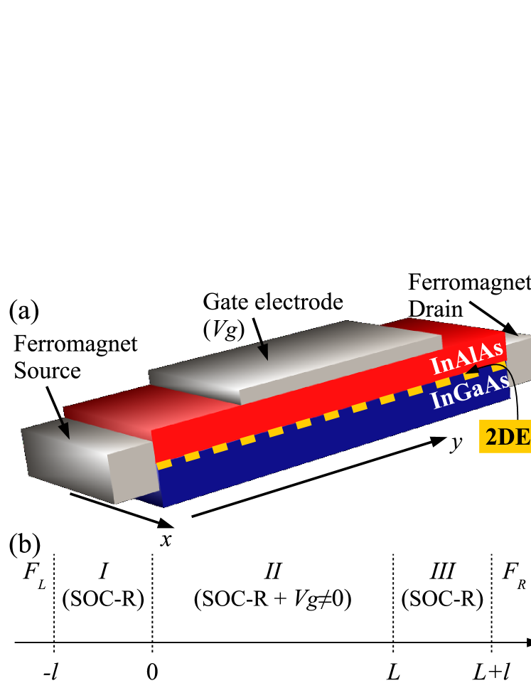
The strength of SOC-R can be tuned by external electric fields Nitta et al. (2009), which imply a gate mechanism for spin-based transistors Datta and Das (1990); Schliemann, Egues, and Loss (2003); Shelykh, Galkin, and Bagraev (2005); Chuang et al. (2015). Datta and Das spin field effect transistor (SFET) Datta and Das (1990) (Fig. 1) is a theoretical device, conceptually similar to an electro-optic modulator. Two ferromagnets act as polarizer and analyzer. The propagation medium between them —capable of inducing a gate-controllable net rotation of the spin orientation via SOC-R— is a two-dimensional electron gas (2DEG).
Spin-dependent conductance in SFET-like systems has been widely addressed Mireles and Kirczenow (2001, 2002); Pala et al. (2004a, b); Yang et al. (2008); Gao, Lundstrom, and Nikonov (2011); Pareek and Bruno (2002); Wu et al. (2003). In 2001, Mireles and Kirczenow Mireles and Kirczenow (2001) perform calculations of spin-dependent ballistic transport properties in quantum wires, in the presence of SOC-R. Using a tight-binding scheme, they showed that a strong SOC-R may lead to dramatic changes in the transmission of electrons. The transport of holes in -doped hybrid (magnetic and nonmagnetic) structures was considered by Pala et al. Pala et al. (2004a, b), exhibiting clear possibilities of current manipulation. The effects of the temperature Mireles and Kirczenow (2002), external magnetic fields Yang et al. (2008) and the direction of magnetization at the polarizer and analyzer electrodes Yang et al. (2008); Pareek and Bruno (2002); Pala et al. (2004a) have also been addressed. Recently, Gao et al. Gao, Lundstrom, and Nikonov (2011) carried out a simulation of a SFET, based on the nonequilibrium Green’s function formalism self-consistently coupled with a Poisson solver to produce the device characteristics, obtaining good agreement with the recent experiments. However, these studies does not allow for the modifications in the opacity of the propagation medium that itinerant electrons feel when the gate-voltage is switched, as we will discuss later.
Another issue insufficiently investigated is the spin-dependent tunneling time in SFET-like systems. As far as we know, only few studies have focused the quantum transport time under SOC-R in ferromagnetic/semiconductor/ferromagnetic systems. Based on the group velocity concept, Wu et al. Wu et al. (2003) showed that as the strength of the SOC-R increases, the traversal time considerably decreases and exhibits step-like behavior when the length of the channel growths. However, it should be pointed out that SOC-R appears in the system they are modelling as a consequence of an asymmetry introduced at the ferromagnetic/semiconductor interface to fix some known problems related with the efficiency of the spin-injection. Then, as the potential gradient in this case is parallel to the transmission direction, the effective magnetic field is null. Hence, there is not spin-precession, in contrast to SFET-like systems where the potential gradient induced by the gate electrode is perpendicular to the transmission direction.
This contribution focuses on the quantum transport properties in SFET-like devices. Using a simple modelling, combined with a suitable algorithm of solution, we show that spin-depend conductance exhibits the general features reported before, but strongly modulated by dispersive effects, appearing when the SOC-R coupling parameter is tuned via external electric fields. Although we demonstrate that the transport time —using the phase time concept— may not be spin-resolved, our simulation allows us to evaluate the spin-flip time, which is an important time scale for spintronics applications, together with the spin relaxation and decoherence times.
The remaining part of this paper is organized as follows: Sec. II is devoted to describe the physical system and the theoretical formalism describing electrons in SFET-like systems. The general properties of the simulation procedure are presented in Sec. III. In Sec. IV we discuss numerical results of spin-dependent conductance and phase time. Finally, in Sec. V, we underline some concluding remarks.
II Theoretical Model
We simulate the device depicted in Fig. 1 by a five regions system: and correspond to the ferromagnets, whereas () and stand for the free and gate-managed regions, respectively. The 2DEG is confined at the interface of a heterostructure, InAlAs/InGaAs for instance, where SIA lead to Rashba coupling. Spin-polarized electrons are injected by an ideal ferromagnet from the region . Another ideal ferromagnet allows identifying the spin direction of the right side outgoing electrons. By “ideal” we overlook the actual limitations of ferromagnets Schmidt et al. (2000); Rashba (2000), fixing the initial electrons spin polarization instead. For simplicity, we choose the same effective mass along the whole system.
The []-plane total Hamiltonian for a 2DEG confined on it, has the form Mireles and Kirczenow (2001)
| (1) |
Here we have introduced an extra term , standing for the bounded states at the direction. In the infinite triangular well approximation to the heterostructure confining potential de Andrada e Silva, La Rocca, and Bassani (1994); Cuan and Diago-Cisneros (2011), are given by
| (2) |
where are zeros of Airy function (, , , …), and the electric field due to SIA. Note that involves both intrinsic —density () dependent— and external () contributions.
The off-diagonal terms in (1) correspond to the SOC-R, where is the coupling parameter de Andrada e Silva, La Rocca, and Bassani (1994)
| (3) |
and are the gap and splitt-off energies, respectively.
Because of Rashba coupling, the eigenvalue problem for the Hamiltonian (1) produces two branches in the dispersion relations
| (4) |
where , and eigenvectors
| (5) |
with .
Hamiltonian (1) is time-reversal invariant, therefore it can not support spontaneous spin polarization of the electron states Mireles and Kirczenow (2001). However, it is capable of removing the spin degeneracy for through an effective magnetic filed Ganichev et al. (2004) , with as the Bohr magneton.
III Multicomponent Scattering Approach
Weakly coupled multi-mode quantum transport of electrons has been typically treated through one-dimensional single-mode approximations. The corresponding solutions, along with the envelope function approximation, are multicomponent wave functions. However, it is usual Wessel and Altarelli (1989); Kumar, Cahay, and Roenker (1997) to arbitrarily cancel all components but one in order to compute transmission coefficients, which may lead to lose valuable physical information. Recently, an alternative formalism, named Multicomponent Scattering Approach (MSA), has been proposed (See Refs. Diago-Cisneros et al. (2002, 2006, 2007); Arias-Laso and Diago-Cisneros (2012) for details). MSA takes into account —jointly and simultaneously— all the propagating modes, then a multicomponent description of transmission amplitudes is carried out in a natural way.
Let
| (6) |
be the general solution of the system described by the Hamiltonian (1). To introduce the transfer matrices we define the bi-vector
| (7) |
and the state vector
| (8) |
include the wave vectors and their derivative. The coefficients and are matrices (). and are bidimensional vectors, whose components describe a propagating or evanescent mode, according to the energy.
Based on the above definitions and taking into account that solutions (6) are plane-waves, it is possible to establish the crucial relation
| (9) |
The matrix depends on the specific Hamiltonian, and is build up using the property . In our particular case we have
| (10) |
being .
The first-kind transfer matrix ( stands for function and derivative), which relates the solutions and their derivative (7) between two points of the system and , is defined by
| (11) |
Likewise, the second-kind transfer matrix ( stands for state vector), which relates the sate vectors (8), is defined by
| (12) |
These matrices satisfy the relevant physical properties and symmetries of the Hamiltonian (1).
Using equations (7)-(12) the transformation
| (13) |
is obtained, which relates the two types of transfer matrices already defined.
Following the transfer matrix and scattering matrix definitions we can establish
| (14) |
and
| (15) |
respectively, where and ( and ) are transmission and reflection amplitudes for left (right) incident particles. Using (14) and (15) together with the imposed boundary conditions it is possible to relate the scattering amplitudes for the symplectic caseMello, Pereyra, and Kumar (1988); Diago-Cisneros et al. (2006)
| (16) |
The connection between Transfer Matrix and Scattering Matrix formalisms is the most remarkable feature of MSA.
From relations (16) we could obtain relevant transport magnitudes. Considering the incidence of particles from the left only, the transmission coefficient from channel to channel is given by
| (17) |
Furthermore, they allow to compute the conductance through the channel
| (18) |
the two-probe Landauer conductance
| (19) |
the phase-transmission amplitudes
| (20) |
and the phase-transmission times or group delays
| (21) |
IV Spin-dependent transport properties
Our gedanken experiment consists of introducing spin-polarized electrons in the three-region channel with SOC-R (, and in Fig. 1 (b)), under normal incidence (). We are able to tune up the coupling parameter in the central region (region , below the gate electrode), the length of this region and the energy of the incident electrons. We set the length of the regions and as nm. SOC-R in these regions is solely given by the intrinsic asymmetry of the confining potential, which depends on the surface charge density, cm-2, from now on. Following the Landauer picture Imry and Landauer (1999), we assume the whole system connected to infinite reservoirs of charge at different chemical potential, avoiding the inclusion of an external electric field to move electrons along the system.
There are two direct paths connecting electrons with the same spin ( and ) and two crossed paths connecting electrons with different spin ( and ). The availability of the last two is given by the SOC-R. In accordance with our consideration for regions and , we are only interested in the paths and because we are injecting in the channel only spin- polarized electrons.
Taking as energy reference the first transversal state —given by Exp. (2)— electrons traveling from region into experience a potential barrier of height
| (22) |
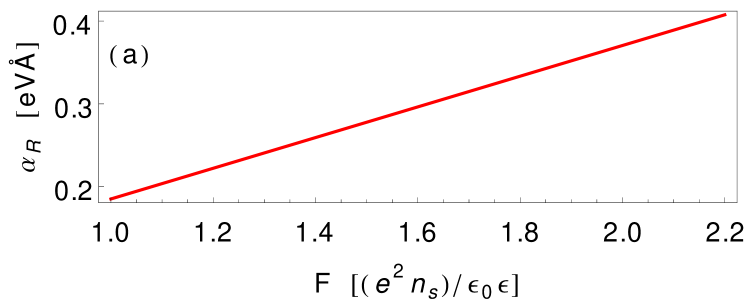
and thickness , due to the mismatch of the energy levels between those regions, induced by the external electric field. Then, the potential essentially depends on the voltage at the gate electrode (region , see Fig. 1). Hence, by tunning the height of this barrier also changes, as shown Fig. 2. The coupling parameter growths following (3) (see panel (a)), while growths following (22) (see panel (b)).
It is a well-known result Mireles and Kirczenow (2001, 2002); Pala et al. (2004a) that spin-resolved conductance oscillates with the lengthening of the channel, due to the SOC-R-induced spin precession phenomenon. In fact, assuming that electrons move freely (fill no potential barrier (22)) along the positive direction in the transport channel, following (4)-(5), the equivalent wave function would be
| (23) |
where and are the positive solutions of equations (4). Consequently, the probability of detecting spin- or spin- electrons at a given reads Mireles and Kirczenow (2001)
| (24) |
| (25) |
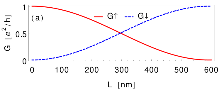
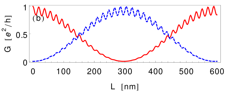
respectively. The oscillations are then straightforward from the presence of cosine and sine functions. This behavior is observed in our calculations, as a general trend (see Fig. 3).
Both SFET operating points are shown in the panels (a) and (b) of Fig. 3, respectively. Fixing the polarization of incoming electrons along the direction for convenience, at null gate-voltage the intrinsic asymmetry of the heterostructure potential ensures that spin-up conductance (associated with the path ) vanishes for nm (Fig. 3 (a), red solid line). Hence, by conservation low, the spin-down polarized total outgoing flux maximizes (, Fig. 3 (a), blue dashed line) but being associated with the path , becomes forbidden by the ferromagnetic analyzer, and then the device is closed. On the other hand, for a suitable value of the gate-voltage that strengthens the electric field 2.2 times respect to the one at the bare regions (), the conductance for spin-up polarized electrons is magnified ( and ), as shown in Fig. 3 (b) (red solid and blue dashed lines, respectively). In this case, the ferromagnetic analyzer allows the transport, thereby the device is opened. This two-states behavior of the SFET had been proposed Ladd et al. (2010) for codifying and manipulating information (“” and “” values of a bit) instead of the current field effect transistors.
At a given value of the Fermi energy, by evaluating and in Exps. (4) we have , then
| (26) |
From (26) it is straightforward to note that (24) and (25) do not depend on the energy Mireles and Kirczenow (2001), therefore the consequences of changing the energy on the spin-resolved conductance are typically leaved out. In our modelling, the energy plays a crucial role because we do consider the dispersive effects of the constriction at the region (see (22) and its discussion). Actually, the additional “noise” —fast oscillations— in spin-resolved conductance curves, at finite values of the gate-voltage (Fig. 3 (b)), is clearly related with this. To evaluate the significance of those effects, in Fig. 4 we plot the spin-resolved conductance in a particular range of energy, setting all parameters as in Fig. 3 (b). The gate-voltage induced potential barrier (22) has the height , which is lower than the whole energy range considered, then in principle is not tunneling but transmission the quantum phenomenon we are considered. Note that the total conductance, , could be reduced from 75% down to 25%. The existence of resonant peaks is a well-known phenomenon, associated to the condition , where is an integer.
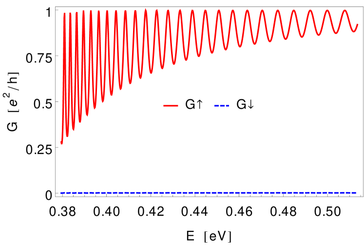
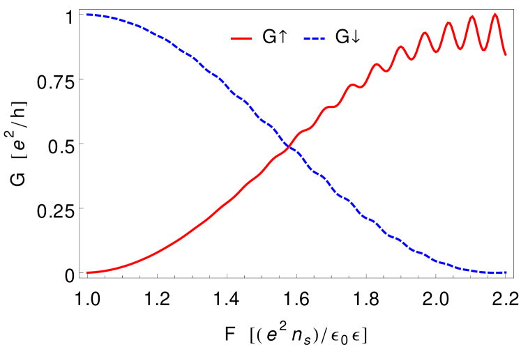
Fig. 5 displays the spin-resolved conductance as function of the electric field at the region II (induced by the gate electrode), in units of the one at the bare regions (I and III). This ()-like curve characterizes the behavior of the modeled SFET. Note that for the outgoing flux is spin- polarized, leading to a closed state, while for is spin- polarized, leading to an opened state. We chose the energy of the incoming spin- polarized electrons as eV, in order to avoid the zone of large-amplitude oscillations of the spin-resolved conductance (see Fig. 4). Even that, for the highest values of the electric field () those oscillations are observed.
We are interested now in evaluating the quantum transport time in the system we are modelling (see Fig. 1). To answer how long it takes an electron to pass through a quantum system is still a controversial question Landauer and Martin (1994). Phase time, defined as in (21), is a well-established definition of this time, and has been extensively used in researches regarding quantum tunneling Steinberg, Kwiat, and Chiao (1993); Winful (2003); Diago-Cisneros et al. (2006, 2007); Arias-Laso and Diago-Cisneros (2012).
The first task then is to compute the phase as function of the energy following (20). Although not shown here, if one plots the phase for the allowed paths, () and (), one may note that the corresponding curves are shifted in the energy. This is consistent with the fact that electrons with different spin polarization propagate along the system with different quasi-momentum, as in the “toy model” described by the solution (23). Consequently, those curves have equal derivative and the phase time is the same along the direct and crossed paths. This may be explained taking into account that manipulation of spins in a SFET via SOC-R —in itself— is not a dispersion-selective phenomenon thus the coherence is preserved. The opposite picture occurs in ferromagnets or dilute magnetic semiconductors, where spin separation features in time have been reported Guo et al. (2001); Wang, Guo, and Gu (2002). A simple modelling of those systems Pala et al. (2004a); Yang et al. (2008) predicts that they behave as a potential barrier for a particular spin polarization and as a potential well for the other, resembling an effective Zeeman splitting.
Fig. 6 displays the phase time as function of the electric field at the region II for two particular values of the energy, eV (squares) and eV (circles). At first sight, one may note that the phase time is lower for the higher energy and its value increases as a general trend in both cases, when one lets the electric field growths. This is intuitively understandable noting that the height of the potential barrier (22) also growths, as shown in Fig. 2 (b). However, no significant changes are observed in for eV when one switches the device from the closed state (, depicted in Fig. 3 (a)) to the opened state (, depicted in Fig. 3 (b)). On the other hand, for eV, varies from ps to ps, which may be quite undesirable for practical applications. Another interesting issue here is the presence of oscillations in both curves, being more evident for eV. These oscillations have been reported before in the case of holes Diago-Cisneros et al. (2007); Arias-Laso and Diago-Cisneros (2012), but as a function of the energy for values above the potential barrier, therefore they have the same nature that the ones we are reporting here.
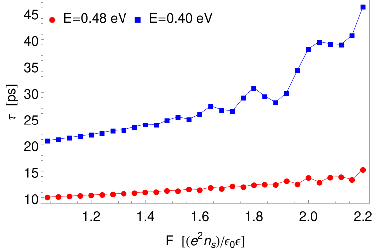
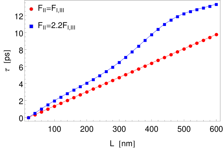
In Fig. 7 we plot as function of the length of the region under SOC-R (region ) for both closed (, circles) and opened (, squares) states, with eV. Note that for nm, which is a kind of spin-flip length for cm-2 (see Fig. 3 (a)), the phase time for the opened and closed states barely differs in ps. While the phase time growths linearly with for (zero gate-voltage), exhibiting a classical-like behavior (), it follow a non-trivial increment when . From Figs. 6 and 7 we may infer that characteristic times governing the operations of the device we are modelling are ps, while the spin relaxation time is typically in the order of nanoseconds Balocchi et al. (2011).
It should be mentioned that is the first time that MSA formalism deal with systems of hundreds of nanometers, which is the typical scale length where spin-flip occurs Mireles and Kirczenow (2001); Pala et al. (2004a); Yang et al. (2008). So far, the magnitudes (17)-(21) had been successfully studied using MSA in systems with length ranging form Å up to Å. General properties, as the probability flux conservation through our system, was verified during the simulations. All physical parameters not mentioned above are referred to In0.53Ga0.47As Vurgaftman, Meyer, and Ram-Mohan (2001).
V Conclusions
The changes in the Datta-Das spin-transistor propagation medium opacity, given by the manipulation of the SOC-R strength, may considerably reduce the conductance of the device. The spin-resolved conductance have exhibited oscillations as expected, but modulated by dispersive effects when the gate-voltage was turned on, leading to significant reduction of the total tunneling conductance. Nonetheless, in a zero temperature picture, present simulation allows us to identify suitable topological and external parameters, to obtain the operating points of the SFET and to prove its feasibility as substitute for current field effect transistors. Although we demonstrate that phase time may not be spin-resolved, we were able to evaluate the time that takes a spin- polarized electron to switch it down, resulting in a range of ps, an order of magnitude lower than typical values of the spin relaxation times. The systematical procedure carried out here, provides the basis for studying novel SFET-like configurations Chuang et al. (2015) and/or addressing -doped SFET-like systems where the phenomenology is strikingly different respect to the electronic case Winkler . A work devoted to those issues is in progress and will be published elsewhere.
References
- Awschalom and Flatté (2007) D. D. Awschalom and M. E. Flatté, Nature Phys. 3, 153 (2007).
- Chen and Buyanova (2014) W. M. Chen and I. A. Buyanova, eds., Handbook of Spintronic Semiconductors (Pan Stanford Publishing, Singapore, 2014).
- Bychkov and Rashba (1984a) Y. A. Bychkov and E. I. Rashba, J. Phys. C: Solid State Phys. 17, 6039 (1984a).
- Bychkov and Rashba (1984b) Y. A. Bychkov and E. I. Rashba, JETP Lett. 39, 2 (1984b).
- (5) R. Winkler, Spin-orbit coupling effects in two-dimensional electron and hole systems (Springer-Verlag, Berlin Heidelberg, 2003).
- Nitta et al. (2009) J. Nitta, T. Bergsten, Y. Kunihashi, and M. Kohda, J. Appl. Phys 105, 122402 (2009).
- Datta and Das (1990) S. Datta and B. Das, Appl. Phys. Lett. 56, 665 (1990).
- Schliemann, Egues, and Loss (2003) J. Schliemann, J. C. Egues, and D. Loss, Phys. Rev. Lett. 90, 146801 (2003).
- Shelykh, Galkin, and Bagraev (2005) I. A. Shelykh, N. G. Galkin, and N. T. Bagraev, Phys. Rev. B 72, 235316 (2005).
- Chuang et al. (2015) P. Chuang, S. C. Ho, L. W. Smith, F. Sfigakis, M. Pepper, C. H. Chen, J. C. Fan, J. P. Griffiths, I. Farrer, H. E. Beere, G. A. C. Jones, D. A. Ritchie, and T. M. Chen, Nat. Nanotechnol. 10, 35 (2015).
- Mireles and Kirczenow (2001) F. Mireles and G. Kirczenow, Phys. Rev. B 64, 024426 (2001).
- Mireles and Kirczenow (2002) F. Mireles and G. Kirczenow, Phys. Rev. B 66, 214415 (2002).
- Pala et al. (2004a) M. G. Pala, M. Governale, J. König, U. Zülicke, and G. Iannaccone, Phys. Rev. B 69, 045304 (2004a).
- Pala et al. (2004b) M. G. Pala, M. Governale, J. König, and U. Zülicke, Europhys. Lett. 65, 850 (2004b).
- Yang et al. (2008) J. Yang, C. Lei, C. Rong, and K. M. Jiang, Eur. Phys. J. B 62, 263 (2008).
- Gao, Lundstrom, and Nikonov (2011) Y. Gao, M. S. Lundstrom, and D. E. Nikonov, J. Appl. Phys 109, 07C306 (2011).
- Pareek and Bruno (2002) T. P. Pareek and P. Bruno, Pramana 58, 293 (2002).
- Wu et al. (2003) H. C. Wu, Y. Guo, X. Y. Chen, and B. L. Gu, J. Appl. Phys. 93, 5316 (2003).
- Schmidt et al. (2000) G. Schmidt, D. Ferrand, L. W. Molenkamp, A. T. Filip, and B. J. van Wees, Phys. Rev. B 62, R4790 (2000).
- Rashba (2000) E. I. Rashba, Phys. Rev. B 62, R16267 (2000).
- de Andrada e Silva, La Rocca, and Bassani (1994) E. A. de Andrada e Silva, G. C. La Rocca, and F. Bassani, Phys. Rev. B 50, 8523 (1994).
- Cuan and Diago-Cisneros (2011) R. Cuan and L. Diago-Cisneros, J. Appl. Phys 110, 113705 (2011).
- Ganichev et al. (2004) S. D. Ganichev, V. V. Bel’kov, L. E. Golub, E. L. Ivchenko, P. Schneider, S. Giglberger, J. Eroms, J. De Boeck, G. Borghs, W. Wegscheider, D. Weiss, and W. Prettl, Phys. Rev. Lett. 92, 256601 (2004).
- Wessel and Altarelli (1989) R. Wessel and M. Altarelli, Phys. Rev. B 39, 12802 (1989).
- Kumar, Cahay, and Roenker (1997) T. Kumar, M. Cahay, and K. Roenker, Phys. Rev. B 56, 4836 (1997).
- Diago-Cisneros et al. (2002) L. Diago-Cisneros, P. Pereyra, R. Pérez-Álvarez, and H. Rodríguez-Coppola, Phys. Stat. Sol. (b) 1, 125 (2002).
- Diago-Cisneros et al. (2006) L. Diago-Cisneros, H. Rodríguez-Coppola, R. Pérez-Álvarez, and P. Pereyra, Phys. Rev. B 74, 045308 (2006).
- Diago-Cisneros et al. (2007) L. Diago-Cisneros, H. Rodríguez-Coppola, R. Pérez-Álvarez, and P. Pereyra, Rev. Mex. Fís 53, 7 (2007).
- Arias-Laso and Diago-Cisneros (2012) S. Arias-Laso and L. Diago-Cisneros, Physica E 44, 1730 (2012).
- Mello, Pereyra, and Kumar (1988) P. Mello, P. Pereyra, and N. Kumar, Ann. Phys. (N.Y.) 181, 290 (1988).
- Imry and Landauer (1999) Y. Imry and R. Landauer, Rev. Mod. Phys. 71, S306 (1999).
- Ladd et al. (2010) T. D. Ladd, F. Jelezko, R. Laflamme, Y. Nakamura, C. Monroe, and J. L. O’Brien, Nature 464, 45 (2010).
- Landauer and Martin (1994) R. Landauer and T. Martin, Rev. Mod. Phys. 66, 217 (1994).
- Steinberg, Kwiat, and Chiao (1993) A. Steinberg, P. Kwiat, and R. Chiao, Phys. Rev. Lett. 71, 708 (1993).
- Winful (2003) H. Winful, Phys. Rev. Lett. 91, 260401 (2003).
- Guo et al. (2001) Y. Guo, B. Wang, B. L. Gu, and Kawazoe, Phys. Lett. A 291, 453 (2001).
- Wang, Guo, and Gu (2002) B. Wang, Y. Guo, and B. L. Gu, J. Appl. Phys. 91, 1318 (2002).
- Balocchi et al. (2011) A. Balocchi, Q. H. Duong, P. Renucci, B. L. Liu, C. Fontaine, T. Amand, D. Lagarde, and X. Marie, Phys. Rev. Lett. 107, 136604 (2011).
- Vurgaftman, Meyer, and Ram-Mohan (2001) I. Vurgaftman, J. R. Meyer, and L. R. Ram-Mohan, J. Appl. Phys 89, 5815 (2001).