Defect controlled vortex generation in current-carrying narrow superconducting strips
Abstract
We experimentally study effect of single circular hole on the critical current of narrow superconducting strip with width much smaller than Pearl penetration depth . We found nonmonotonous dependence of on the location of a hole across the strip and a weak dependence of on radius of hole has been found in case of hole with ( is a superconducting coherence length) which is placed in the center of strip. The observed effects are caused by competition of two mechanisms of destruction of superconductivity - the entrance of vortex via edge of the strip and the nucleation of the vortex-antivortex pair near the hole. The mechanisms are clearly distinguishable by difference in dependence of on weak magnetic field.
I Introduction
The maximal current, which can pass through the superconducting strip without dissipation, is equal to , where is a width and is a thickness of the strip and is the depairing current density. However in experiments, this value can be reached only in relatively thin (, is the magnetic field penetration depth) and narrow strips with in which a current density is distributed uniformly across the width and thickness Likharev . In opposite situation of wide and thick strips (, ), an expelling of magnetic field, which is induced by an applied current, from the interior of the strip leads to piling up of current density at the edge of strip and the maximal critical current becomes smaller than . Moreover, even in the narrow and thin superconducting strips with uniformly distributed current density the measured critical current is smaller than JETP_Andr ; PRB_Rusanov ; Nawaz . The suppression of experimentally measured critical current in such structures can be explained by a presence of defects in the strip. Under defect we understand a local perturbation of properties of the strip which provides a local suppression (complete or partial) of the superconducting order parameter in the current-carrying state of the strip. This local suppression of can be due to local variation of the thickness/width of the strip, its material parameters such as the electron mean path and/or critical temperature or such suppression of may appear temporally in the place of absorption of high energetic photons or particles. The superconducting current avoids the place with suppressed and this phenomenon leads to nonuniform current distribution, with the maximal current density near the defect place. Now this phenomenon is known as a current crowding effect, which was studied in details theoretically in C&B and confirmed experimentally in Henrich ; Hort ; Adami ; Akh on model systems of narrow strips with sharp bends which play a role of defects.
In the recent theoretical work SUST_DV , the effect of a single defect, which is located close or far from the edge of the superconducting strip with finite width, on generation of resistive state was studied in frame of Ginzburg-Landau approach. The defect was modelled by the circle with locally suppressed superconductivity - we call it later as a ’hole’. It has been shown that the mechanism of destruction of superconducting state by applied current in a narrow strip depends on position of the hole with respect to the edge of strip. When the hole sits close to the edge, the self-generated vortices enter the hole via the edge of the film and then they move across the superconductor. In this sense it resembles effect of edge defect Buzdin ; Melnikov ; Vodolazov_def ; Koshelev . When the hole is located pretty far from the edges, the vortex-antivortex pair is nucleated inside the hole and a motion of the pair destroys the superconducting state JETP_1983 ; SUST_DV . Domination of the first or the second mechanism of destruction of superconductivity leads to extremely nonmonotonic dependence of critical current on the position of the hole (see Fig. 4 in Ref. SUST_DV ).
The interesting effects arise when the hole is located in the center of strip. First of all the theory predicts that in a certain range of the hole’s radius the critical current is independent of and equals to about C&B ; PRB_DV_Z . This counterintuitive result (one could expect that in case of uniform current distribution near the hole and when ) is the direct consequence of the current crowding near the circular hole. Secondly, in this particular situation the small magnetic field weakly affects the critical current in comparison to a strip without hole. This weakening of the dependence is because the resistive state is determined by the vortex-antivortex nucleation near the hole and not at the edges of a strip where Meissner currents are maximal. Moreover, due to opposite direction of the generated Meissner currents at the opposite edges of strip, the influence of external magnetic field on of strips is dependent on location of the hole. This effect leads to increase of when the hole is near to one of the edges and to decrease of when the hole is at the opposite edge (see Fig. 9 in SUST_DV ).
We stress here the difference between the effect of defects at relatively large magnetic field (when there is dense vortex matter in the strip) and at zero or small magnetic fields (when there is no field induced vortices) in current-carrying superconductors. In the former case, the vortices, which are created by the externally applied magnetic field, can be effectively pinned by defects and, thereby, this strengthens transport properties of superconductor. Pinning by intrinsic and artificially created defects has been extensively studied in numerous theoretical and experimental works Reichhardt ; Castellanos ; Velez . In the case of small or even zero magnetic field, the superconductivity is weakened near the defect due to current crowding. When the applied current exceeds some critical value the vortices are nucleated near this weak place and their motion destroys the superconducting state JETP_1983 ; SUST_DV .
Comparison of the theoretical predictions SUST_DV with experimental results, which are obtained in real structures, is complicated. It is very difficult to find a single natural (intrinsic) defect in a film which localizes far enough from a lot of other similar defects and then arrange experiment to study transport properties which are determined by this particular defect and are not smeared out by collective effect of other defects. In case of local suppression of superconductivity caused by absorbed photon, deterministic localization of absorption site is not possible at all due to probabilistic nature of the photon absorption.
In the present work we made holes of different size and placed them in different places across the superconducting strip. Such a model system mimics the main effect of the real defect - current crowding effect and it allows us in controllable manner to study the role of the defects on the critical current and mechanisms of destruction of the superconducting state.
We have experimentally found the non-monotonous dependence of of strips with the hole with constant radius on the position of this hole with respect to the edge of the strip. We have also shown that the dependence of on weak magnetic fields in case of mechanism of vortex-antivortex nucleation in vicinity of the hole is weaker than the -dependence which is determined by a single-vortex penetration through the edge of superconducting strip in agreement with theoretical predictions SUST_DV . Our results allow not only to clarify the role of defects on suppression of the critical current at zero and low magnetic fields (, Meissner state) but they also help to understand the mechanism of photon detection by current-carrying superconducting strips.
II Experiment
NbN films with thickness about 5 nm were deposited on a heated sapphire substrate by DC reactive magnetron sputtering of pure Nb target in a gas mixture atmosphere of argon and nitrogen. For the used deposition conditions of the total pressure 2.8 mbar, partial pressure of nitrogen 3.2 mbar and sputter current 150 mA, films with the critical temperature 13 K, square resistance of about 300 Ohm and residual resistance ratio RRR = 0.89 were deposited.
Patterning of films has been done by electron-beam lithography and ion-milling technique. The films were patterned into single-bridge structures with a width about 1 m and a length 20 m which were embedded between two millimeter sized contact pads. The gradual transition between the bridge and the contacts with radius of curvature = 5 m was realized to avoid a current crowding at T-shape connections which were considered in details in C&B .
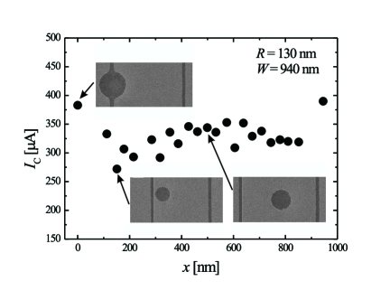
Two series of samples (24 bridges each) have been fabricated on separated 10 mm squared chips. In the first series of samples, circle with radius 130 nm was etched inside a bridge. The etched circles were always placed at a half-length of bridge. The coordinate of circles across the width of bridge was varied with respect to the left edge of bridge with a step 35 nm between two subsequent positions (see the insets in Fig. 2). Through the paper samples which belong to this series of bridges will be named XNN where NN is a distance in nanometer between left edge of a strip and center of a hole which is etched inside the strip. The radius of circles with a center placed at the edge of bridges (in this case it is better to talk about semi-circles, see the top left inset in Fig. 2) was by a factor larger i.e. about 185 nm. This was done to keep constant the area with suppressed order parameter independently of location of the hole.
In the second series of samples, the position of etched circle (the hole) was kept constant in the middle (half-length, half-width) of a strip but the radius of hole was varied by an order of magnitude from about 29 nm up to 225 nm. In the paper, samples, which belong to this series, will be named RNN where NN is a radius of etched hole in nanometer. Real dimensions of fabricated structures (width of bridge, , radius of hole, , and its position with respect to the left edge of bridge, coordinate ) were measured after patterning by a scanning electron microscopy (SEM).
All bridges were characterized by their critical temperature of superconducting transition. The value was determined as a temperature at which resistance of measured structure drops below 0.1 of the normal state resistance measured at temperatures approximately twice higher than . The obtained spread of among bridges in each series was about 0.3 K which can be attributed to slight variation of superconducting strength over the film caused by, for example, non-uniformity of thickness of deposited film. In case of ultra-thin films with thickness about the coherence length which is in case of NbN is about 4-5 nm PRB14Ilin , even a small difference in thickness leads to relatively large change in PRB09Sem ; PRB13Noat .
The current-voltage characteristics (IV-curves) were measured in a cryogenic-free system at 5.1 K in a DC current-bias mode. The magnetic field up to 1 T generating by a superconducting solenoid was applied normally to a sample surface. From the previous studies PRB14Ilin we know that the field, which is required for penetration of magnetic vortex into a micrometer wide bridge made from thin NbN film, is in the range of few tens millitesla and therefore the available in our experiments range of is enough for detailed investigations of bridges in Meissner and in the vortex states. The minimum step of variation of magnetic field was 1 mT which is determined by accuracy and stability of a used power supply of superconducting solenoid.
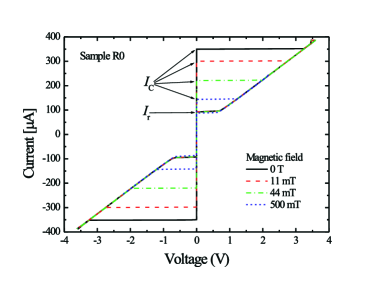
Typical IV-curves for four different magnetic fields are shown in Fig.1. The curves were hysteretic independently of the magnetic fields in the whole range of applied fields . At a critical current , the bridge is characterized by a sharp jump from superconducting to normal state. Recovery of superconductivity in the bridge happens at current which is almost independent of magnetic field as it is clearly seen in Fig. 1. Contrary, demonstrates significant decrease with increase of the applied field. The accuracy of determination in our experimental setup is 0.5 of , i.e. about 1 A for studied range of critical currents.
III Results
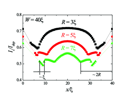
The experimentally obtained dependence of the critical current on position of the hole is shown in Fig. 2. It is seen that is maximal when the hole is in the middle of the strip and when the hole (semi-circle) is placed at the edge of the strip. Shift of position of the hole from the center of the strip leads to gradual decrease of which reaches the minimum values when the hole is close to the edge. This experimental result qualitatively coincides with the prediction of Ref. SUST_DV . In Fig. 3 we present results of theoretical calculations which were performed in the framework of Ginzburg-Landau model for different holes and strip with (details of numerical calculations are present in Ref. SUST_DV ). In contrast to Ref. SUST_DV we determine the critical current as the current at which permanent vortex flow starts in the strip with a hole. In Ref. SUST_DV was defined as the current at which the first vortex enters the hole when it is located near the edge of the strip - due to assumption that the ’hole’ is created by the absorbed photon and it should dissolves after some finite time interval. New definition leads only to quantitative difference with result of Ref. SUST_DV : i) the local minimum in dependence now reaches when the hole sits on the finite distance from the edge; ii) additional minima appear when the hole practically touches the edge. These minima appear for relatively wide strips and large radiuses of the holes . The width of the additional minima is about the coherence length (see Fig. 3) and it is rather difficult to resolve it in the experiment due to small nm in NbN. Small width of this minima () points on its origin - it appears due to suppression of the order parameter in the narrow sidewalk between edge of the hole and edge of the strip when its width becomes about (because we model the hole as a region with locally suppressed superconductivity). It results in decrease of the ’superconducting’ width of the strip.
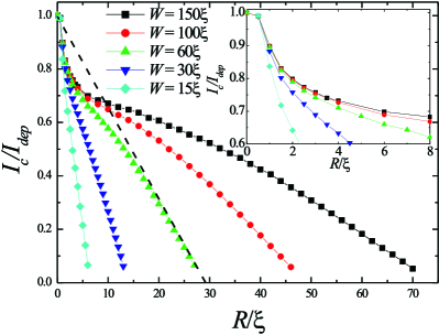
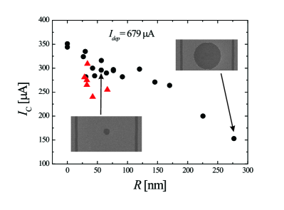
We also studied how depends on the radius of the hole when it is placed in the center of the strip. Theoretical results are present in Fig. 4 while experimental -dependence is shown in Fig. 5. The theory predicts, that when the critical current very weakly depends on (see inset in Fig. 4). Calculations in the London model C&B ; PRB_DV_Z predict that in this case while our numerical results give a little larger value . The difference between theoretical results is most probably connected with the characteristics of the hole. In Refs. C&B ; PRB_DV_Z the hole was considered as a ’well’ with jump of at the edge while in our model, due to proximity effect, changes from zero to its maximal value on the distance near the hole’s edge.
In the experiment we find small variation of A () for holes with radius nm () - see Fig. 5. The depairing current A has been calculated in frame of Ginzburg-Landau theory with account of the temperature dependent correction factor which was obtained by Kupriyanov and Lukichev Kupriyanov for dirty limit superconductors (see Eqs. 3 and 4 in PRB14Ilin ). We have to note, that even for strips without hole (see Fig. 5) due to presence of the intrinsic defects. These defects may be present also at the edge of the hole which additionally suppresses the critical current and it could be a reason for dispersion of for holes with radius nm and smaller value of than expected from the theory.
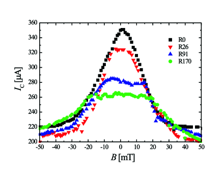
Theory SUST_DV predicts, that when the hole is placed in the center of the strip the resistive state starts via nucleation of the vortex-antivortex pair near the hole. Direct experimental visualization of this process is practically impossible at the present time, due to very short time scale ( picoseconds) of vortex nucleation. However it could be checked indirectly, using external magnetic field . The applied magnetic field induces screening current which is maximal near the edges and it is equal to zero in the center of the strip. Therefore if resistive state is realized via vortex entrance via edge of the film then applied magnetic field strongly influences . Contrary, if resistive state is realized via generation of the vortex-antivortex pairs near the central part of the strip the same magnetic field weakly affects . Experimental -dependencies will differ significantly in dependence on location of penetration of vortex or vortex-antivortex pair and, thereby, can be used for determination of position of vortex generation in the strip at .
In Fig. 6 we show experimental dependencies for strips with and without hole in the center. For samples R26, R91 and R170 ( = 26, 91, 170 nm) there is plateau at low while for strip without hole (sample R0) decays almost linearly at low . Therefore we conclude, that in the sample without the hole the vortices are generated at the edge of the strip while in the samples with the hole the vortex-antivortex pairs are generated near the hole at 5-18 mT (the larger the hole the larger the threshold magnetic field). Magnetic fields larger the threshold produce large screening currents at the edges of the strip which, together with transport current, exceeds the current density near the hole and the vortices start to be generated at the edge. As a result the strong field dependence of is recovered.
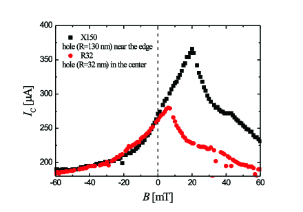
When the hole is located close to the edge of the strip the maximum of -dependence is shifted to the finite magnetic field (sample X150, black squares in Fig. 7). Nearly linear -dependence at low again demonstrates that vortices enter via edges and the shift in is connected with different vortex entry conditions from the left and right edges due to presence of the hole. Note, that such a shift was also observed for strip with central hole (sample R32, red circles in Fig. 7) where it most probably appears due to relatively large intrinsic defect at the left edge of the strip (the location of the defect follows from the direction of the shift in ) .
IV Discussion
There are three main experimental observations which confirm theoretical predictions formulated in Ref. SUST_DV and PRB_DV_Z :
i) the non-monotonic dependence of on coordinate of hole across the width of superconducting strip (Fig. 2);
ii) the dependence of on radius of hole which is placed in the middle of the strip is much weaker than it is expected from geometrical point of view when radius of hole is in the range (Fig. 5);
iii) the weak dependence of on magnetic field at small when the hole is located in the middle of strip (Fig. 6). This weak -dependence is caused by generation of vortex-antivortex (V-A) pairs near the hole due to a current crowding in vicinity of that place. This area is weakly influenced by Meissner currents which are mainly concentrated near edges of strip. Contrary, the strong, linear decrease of with increasing is observed when vortex is generated at the edge of strip. This mechanism dominates over V-A-generation mechanism mostly in strips with holes which are shifted from the center of strip or in strips without any artificial holes (Figs. 6 and 7).
Quantitative deviation from the theory we explain by the presence of the intrinsic defects in real strips. Indeed, some strips without hole has a critical current comparable to of the strip with the hole (see Fig. 5). Because measured suppression of by the circular hole with radius is not large (see Fig. 6) one can imagine situation when intrinsic defect suppresses stronger than circular hole. This result is supported by the measurement of -dependence which demonstrates linear variation of at low magnetic field despite the presence of the hole in the center (for illustration see Fig. 7, sample R32). We believe, that asymmetry of , visible in Fig. 7 for strip with the central hole also comes from the intrinsic defects near the hole or deviation from the circular shape which also breaks mirror symmetry in the superconducting strip.
Although we made our measurements for relatively wide micron size strip we believe that obtained results and their analysis are at least qualitatively valid for narrower strips too. Our numerical calculations show that the shape of -dependence does not change substantially while one keeps the ratio the same and when . Our theoretical investigation shows that in the strips with width the minima of dependence correspond to holes placed on the distance from the edge of the strip which is close to the experimental result for strip with (see Fig. 2).
From Fig. 3 it is also seen that is almost independent of the coordinate in a pretty wide range of in case the smallest hole () which is placed in the vicinity of center of the strip. The plateau in (x)-dependence decreases with increase of and, in case of the largest radius, a sharp maximum of is seen in the middle of strip.
Note, that when radius of the hole and there is relatively strong dependence of on (see inset in Fig. 4). It results in smaller value of for the strip with hole at the edge (in the form of semicircle with radius ) than for the strip with central hole (it could be seen in Fig. 3). For larger radii we have opposite situation (see Fig. 3 and Fig. 2).
Our results could be applied for understanding of some properties of superconducting nanowire single-photon detectors (SNSPD). If one supposes that the absorbed photon creates finite region with suppressed superconductivity and size smaller then then it will influence the critical current of the nanowire in a similar way like holes studied in this work. Our result directly demonstrates that the resistive state will appear at different currents, depending on the place in the strip where the photon was absorbed. Therefore detection efficiency of SNSPD should change monotonically with variation of the current, the effect which was observed in all experiments on SNSPD (see for example recent review Natarajan ).
Acknowledgements.
The work was partially supported by the Russian Foundation for Basic Research (project 15-42-02365/15) and by the Ministry of education and science of the Russian Federation (the agreement of August 27, 2013, N 02. .49.21.0003 between The Ministry of education and science of the Russian Federation and Lobachevsky State University of Nizhni Novgorod).References
- (1) K. K. Likharev, Izv. Vuzov.Radiofizika, 14, 909 (1971); 14, 919 (1971).
- (2) V.P. Andratskii, L.M. Grundel’, V.N. Gubankov, and N.B. Pavlov, Destruction of superconductivity in thin narrow films by a current, Sov. Phys. JETP 38, 797 (1974).
- (3) A. Yu. Rusanov, M. B. S. Hesselberth, and J. Aarts Depairing currents in superconducting films of Nb and amorphous MoGe, Phys. Rev. B 70, 024510 (2004).
- (4) S. Nawaz, R. Arpaia, F. Lombardi, and T. Bauch, Microwave Response of Superconducting YBa2Cu3O7-δ Nanowire Bridges Sustaining the Critical Depairing Current: Evidence of Josephson-like Behavior, Phys. Rev. Lett. 110, 167004 (2013)
- (5) J. R. Clem and K. K. Berggren, Geometry-dependent critical currents in superconducting nanocircuits, Phys. Rev. B 84, 174510 (2011).
- (6) D. Henrich, P. Reichensperger, M. Hofherr, J.M. Meckbach, K. Il’in, M. Siegel, A. Semenov, A. Zotova, D.Yu. Vodolazov, Geometry-induced reduction of the critical current in superconducting nanowires, Phys. Rev. B 86, 144504 (2012).
- (7) H. L. Hortensius, E. F. C.Driessen, T. M. Klapwijk, K.K. Berggren, and J. R. Clem, Appl. Phys. Lett. 100, 182602 (2012).
- (8) O.A. Adami, D. Cerbu, D. Cabosart, M. Motta, J. Cuppens, W.A. Ortiz, V.V. Moshchalkov, B. Hackens, R. Delamare, J. Van de Vondel, A. V. Silhanek, Current crowding effects in superconducting corner-shaped Al microstrips, Appl. Phys. Lett. 102, 052603, (2013).
- (9) M.K. Akhlaghi, H. Atikian, A. Eftekharian, M. Loncar, A.H. Majedi, Reduced dark counts in optimized geometries for superconducting nanowire single photon detectors, Optics Express 20, 23610 (2012).
- (10) A.N. Zotova and D.Y. Vodolazov, Intrinsic detection efficiency of superconducting nanowire single photon detector in the modified hot spot model, Supercond. Sci. Technol. 27, 125001 (2014).
- (11) A. Buzdin and M. Daumens, Electromagnetic pinning of vortices on different types of defects, Physica C 294, 257 (1998).
- (12) A. Yu. Aladyshkin, A. S. Mel’nikov, I. A. Shereshevsky, and I. D. Tokman, Influence of surface irregularities on barriers for vortex entry in type-II superconductors, Physica C 361, 67 (2001).
- (13) D.Y. Vodolazov, I.L. Maksimov, and E.H. Brandt, Vortex entry conditions in type-II superconductors: Effect of surface defects, Physica C, 384, 211 (2003).
- (14) A. E. Koshelev and V. M. Vinokur, Suppression of surface barriers in superconductors by columnar defects, Phys. Rev. B 64, 134518 (2001).
- (15) Yu. M. Ivanchenko, P. N. Mikheenko, New mechanism of penetration of vortices into current-saturated superconducting films, Sov. Phys. JETP 58, 1228 (1983).
- (16) A. N. Zotova and D. Y. Vodolazov, Photon detection by current-carrying superconducting film: A time-dependent Ginzburg-Landau approach, Phys. Rev. B 85, 024509 (2012).
- (17) C. Reichhardt, C.J. Olson, F. Nori, Commensurate and incommensurate vortex states in superconductors with periodic pinning arrays, Phys. Rev. B 57, 7937 (1998).
- (18) A. Castellanos, R. Wordenweber, G. Ockenfuss, A.v.d. Hart, K. Keck, Preparation of regular arrays of antidots in YBa2Cu3O7 thin films and observation of vortex lattice matching effects, Appl. Phys. Lett. 71, 962 (1997).
- (19) M. Velez, J.I. Martin, J.E. Villegas, A. Hoffmann, E.M. Gonzalez, J.L. Vicent, Ivan K. Schuller, Superconducting vortex pinning with artificial magnetic nanostructures, JMMM 320, 2547 (2008).
- (20) K. Ilin, D. Henrich, Y. Luck, Y. Liang, and M. Siegel, D. Yu. Vodolazov, Critical current of Nb, NbN, and TaN thin-film bridges with and without geometrical nonuniformities in a magnetic field, Phys. Rev. B 89, 184511 (2014).
- (21) A. Semenov, B. Gunther, U. Bottger, H.-W. Hübers, H. Bartolf, A. Engel, A. Schilling, K. Ilin, M. Siegel, R. Schneider, D. Gerthsen, N.A. Gippius, Optical and transport properties of ultrathin NbN films and nanostructures, Phys. Rev. B 80, 054510 (2009).
- (22) Y. Noat, V. Cherkez, C. Brun, T. Cren, C. Carbillet, F. Debontridder, K. Ilin, M. Siegel, A. Semenov, H.-W. Hübers, and D. Roditchev, Unconventional superconductivity in ultrathin superconducting NbN films studied by scanning tunneling spectroscopy, Phys. Rev. B 88, 014503 (2013).
- (23) M. Yu. Kupriyanov and V. F. Lukichev, Temperature dependence of pair-breaking current in superconductors, Fiz. Nizk. Temp. 6, 445 (1980) [Sov. J. Low Temp. Phys. 6, 210 (1980)].
- (24) C. M. Natarajan, M. G. Tanner, R. H. Hadfield, Superconducting nanowire single-photon detectors: physics and applications, Supercond. Sci. Technol. 25, 063001 (2012).