Identification of excitons, trions and biexcitons in single-layer WS2
Abstract
Single-layer WS2 is a direct-gap semiconductor showing strong excitonic photoluminescence features in the visible spectral range. Here, we present temperature-dependent photoluminescence measurements on mechanically exfoliated single-layer WS2, revealing the existence of neutral and charged excitons at low temperatures as well as at room temperature. By applying a gate voltage, we can electrically control the ratio of excitons and trions and assert a residual n-type doping of our samples. At high excitation densities and low temperatures, an additional peak at energies below the trion dominates the photoluminescence, which we identify as biexciton emission.
In recent years, semiconducting, atomically thin transition metal dichalcogenides (TMDCs) like MoS2, MoSe2, WSe2 and WS2, have emerged as highly interesting materials for the scientific community due to their extraordinary optical Mak et al. (2010) and electrical properties Radisavljevic et al. (2011), including coupled spin-valley effects Mak et al. (2012) and photovoltaic applications Furchi et al. (2014). These molecular layers show strong photoluminescence (PL) peaks in the visible and near-infrared spectral range, as they experience a transition from an indirect gap in bulk and few-layer samples to a direct gap in the single-layer regime Splendiani et al. (2010). The spatial confinement of carriers in a two-dimensional layer and the weak dielectric screening lead to unusually strong excitonic effects Cheiwchanchamnangij and Lambrecht (2012); Berghäuser and Malic (2014), even at room temperature. High exciton binding energies of the order of 0.5 eV have been reported for single-layer WS2 Chernikov et al. (2014); Ye et al. (2014); Zhu et al. (2015); Hanbicki et al. (2015). Besides the charge-neutral exciton (X), i.e., a bound state of an electron and a hole, also charged excitons can be excited in the presence of residual excess charge carriers. These quasiparticles, called trions, consist either of two electrons and one hole (X-) or one electron and two holes (X+). By applying a gate voltage, one can tune the spectral weight of charge-neutral excitons and trions in single-layer MoS2 Mak et al. (2013), MoSe2 Ross et al. (2013), WS2 Zhu et al. (2015) and WSe2 Jones et al. (2013). Additional, lower-energy PL emission peaks are observed in most single-layer TMDCs at low temperatures. These have been attributed to surface-adsorbate-bound excitons in MoS2 Plechinger et al. (2012) and to crystal-defect-bound exciton states in single-layer diselenides Wang et al. (2014a, b). Given the large binding energy of the excitons, the formation of molecular states consisting of two excitons, so-called biexcitons Klingshirn (2007), is to be expected in dichalcogenide single-layers. Biexciton PL emission should be at energies below the exciton emission due to the additional binding energy, in a similar energy range as defect-bound exciton emission. The signature of biexciton emission was recently observed in PL measurements on WSe2 You et al. (2015). Thus, the origin of the lower-energy PL emission peaks in the other semiconducting TMDCs warrants close investigation.
In this work we report on low-temperature PL of mechanically exfoliated single-layer WS2. To date, only a few works exist which report on the observation of excitons and trions in the low-temperature PL spectrum of mechanically exfoliated Scrace et al. (2015); Mitioglu et al. (2013) single-layer WS2. To the best of our knowledge, a thorough analysis of the temperature-dependent PL spectrum is still absent. In contrast to other semiconducting TMDCs, there is no consensus about the assignment of the X and X- PL features in low-temperature PL of single-layer WS2. The aim of this paper is to clarify those issues, and to provide insight into the nature of an additional low-energy peak in the PL spectrum, which is observable at low temperatures. We identify the exciton and the trion peaks in the temperature range from 295 K to 4 K. Our interpretation of the PL spectra is substantiated by gate-dependent PL measurements which allow us to directly control the exciton-trion ratio. Finally, we utilize power-dependent and helicity-resolved PL measurements to show that the low-energy PL peak we observe stems from a superposition of defect-bound exciton and biexciton emission.
Our samples are mechanically exfoliated from bulk WS2 crystals (2d semiconductors inc.) onto a polydimethylsiloxane (PDMS) stamp. Using an optical microscope, we can identify single-layer flakes of WS2 on the PDMS stamp. We then transfer these flakes onto a p-doped Si chip with a 270 nm SiO2 capping layer, applying an all-dry deterministic transfer procedure Castellanos-Gomez et al. (2014). For gate-dependent measurements, we stamp the flakes onto p-doped Si chips with 500 nm thermal oxide and predefined metal contacts manufactured with e-beam lithography. We use the p-doped Si as a backgate. For low-temperature measurements, the samples are mounted in a He-flow cryostat. The cw lasers used for excitation are focussed with a 100x microscope objective onto the sample, the emitted PL is collected by the same microscope objective (backscattering geometry) and guided into a spectrometer with a Peltier-cooled CCD chip. Unless otherwise noted, a 532 nm laser source is utilized. Helicity-resolved measurements are performed using a 561 nm laser, which allows for near-resonant excitation. Further experimental details are published in Ref. Plechinger et al. (2014).
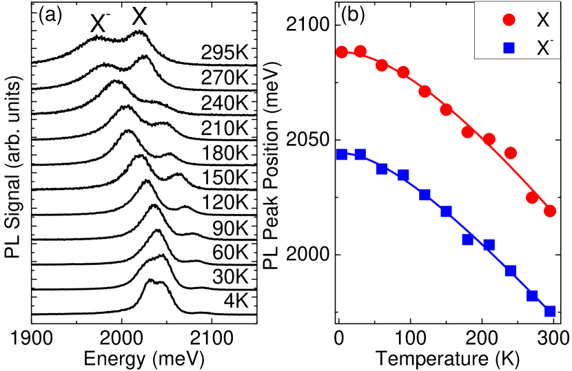
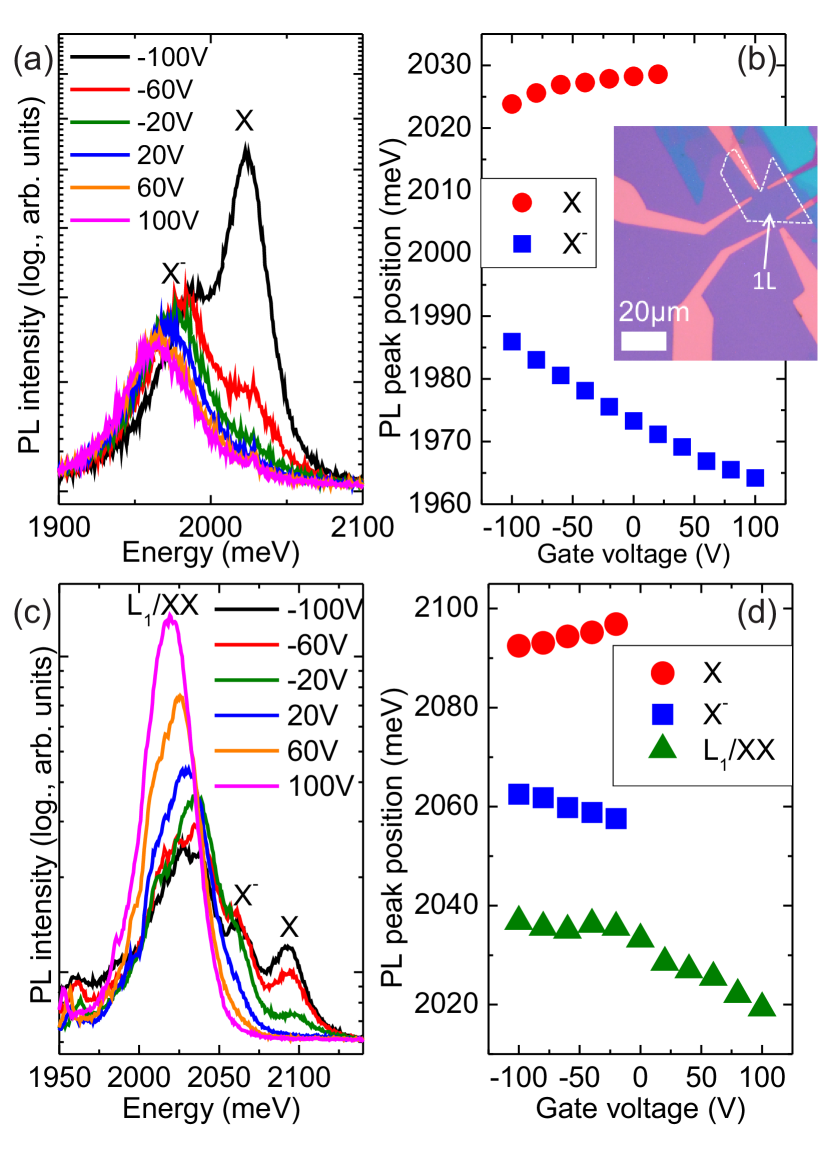
Figure 1(a) shows the PL spectra of single-layer WS2 for various temperatures. In this measurement series, the laser excitation density is kept relatively low at 5 kWcm-2 to avoid possible heating effects. At 295 K, the spectrum consists of two peaks at 2018 meV and 1975 meV, which we attribute to the exciton (X) and the trion (X-). The peak positions at room temperature are in very good agreement with recent reports Zhu et al. (2015); Peimyoo et al. (2014); Bellus et al. (2015). We note that even at room temperature, X and X- peaks can be separated due to their small linewidth. The existence of the trion peak indicates an intrinsic doping of our sample, as it is commonly observed also in other TMDCs Radisavljevic et al. (2011). When cooling down the sample, both PL peaks experience a blueshift in accordance with the Varshni equation Varshni (1967), which describes the change of the bandgap with temperature in a large variety of semiconductors:
| (1) |
where is the bandgap at zero temperature and and are phenomenological fit parameters. We assume that the exciton and trion binding energy are temperature-independent, and that X and X- peaks rigidly shift with the bandgap. We use Eq. 1 to fit the PL peak positions extracted for each temperature, as depicted in Fig. 1(b). For both peaks, the fit matches with eV/K, K and meV for X and meV for X-. The parameters are comparable to those from previous studies on MoS2 Korn et al. (2011). Our assignment of the X and X- peaks at K is further confirmed by additional power-dependent PL measurements at 150 K sup , in which we observe a low-energy tail in the X- peak, which is typical of an electron-recoil effect and has recently also been observed for trions in MoSe2 Ross et al. (2013). The spectral weight shifts from X to X- with decreasing temperature. This indicates that the thermal energy at higher temperatures is large enough to lead to a partial dissociation of the trions. In Fig. 1(a), we also see that the X- peak develops a low-energy shoulder at 30 K and, even more pronounced, at 4 K, which we denominate as L1/XX. We will demonstrate below that it stems from a superposition of defect-bound exciton (L1) and biexciton (XX) emission. In previous reports, either the L1 and L2 peak Mitioglu et al. (2013) or the X- and L1 peak Scrace et al. (2015); Ye et al. (2015), have been attributed to exciton and trion emission. The actual X peak at about 2.09 eV is absent in those studies. The fact that we see a well-pronounced exciton peak in our spectra might be due to our sample preparation process, which leads to a reduced interaction with the substrate in comparison to direct exfoliation of flakes onto SiO2 using adhesive tape.
To confirm our assignment of the exciton and trion peaks, as well as the charge state of the trion, we perform gate-dependent PL measurements. The inset in Fig. 2(b) shows a microscope image of a gated sample. In Fig. 2(a), PL spectra are plotted for different backgate voltages at room temperature. At large negative , the X peak is the dominant one, whereas it is completely suppressed for positive , where the X- peak is the only measurable feature. Hence, we infer that the trions in our samples are negatively charged. This indicates that the WS2 single-layer has a residual n-type doping, similar to MoS2 Radisavljevic et al. (2011) but in contrast to WSe2 Lee et al. (2014). Our room-temperature data is in perfect agreement with Ref. Zhu et al. (2015). Figure 2(c) displays the gate-dependent PL spectra at 4 K. For negative gate voltages, the X peak intensity increases as the Fermi level is shifted towards the neutral regime. This clearly confirms the identification of the 2.088 eV peak as the exciton peak. The X- peak, in contrast, gains in intensity by increasing the gate voltage for . In both gate-voltage dependent measurement series, we observe that the X- peak experiences a spectral redshift, while the X peak shows a slight blueshift with increasing (Fig. 2(b) and (d)), so that the energy difference between X and X- peaks increases with increasing carrier concentration. This effect has also been observed in other TMDCs Mak et al. (2013); Ross et al. (2013). In the limit of low carrier concentration, the ionization energy of a trion is equal to the trion binding energy. In the presence of a 2D electron gas (2DEG), however, ionization of a trion requires that the ionized electron is excited to a state above the Fermi energy of the 2DEG, as all states below the Fermi energy are occupied. Thus, the energy difference between exciton and trion peaks is given by Mak et al. (2013):
| (2) |
with and being the exciton and trion PL peak energies, the trion binding energy and the Fermi energy, which is proportional to . Due to intrinsic doping and the corresponding non-zero , the measured exciton-trion energy difference of 43 meV in the ungated sample shown in Fig. 1(a) is larger than the actual trion binding energy. The exciton-trion peak separation in gated samples follows Eq. 2 sup , showing a minimal peak separation of 30 meV at V. This represents an upper limit for the trion binding energy.
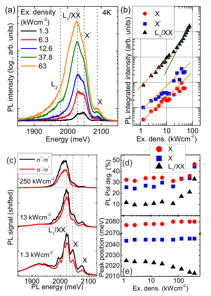
Finally, we focus on the low-energy feature labeled as L1/XX that arises at temperatures below 60 K. Fig. 3(a) shows the PL spectra at K for different excitation powers. Whereas at low powers, X- and L1/XX are spectrally well separated and of similar intensity, at higher excitation powers, the L1/XX peak completely dominates the spectrum. Additionally, a second low-energy peak L2 with moderate intensity is discernible around 1.98 eV. It may stem from defect-bound excitons, as its intensity decreases relative to the other peaks with increasing excitation density. To get a better insight into the nature of the L1/XX peak, we extract the integrated PL intensity for L1/XX, X- and X for different excitation densities, as displayed in the double-logarithmic graph in Fig. 3(b). X and X- show a rather linear behavior indicated by the orange solid line, as expected for an excitonic feature Klingshirn (2007). In contrast, the L1/XX peak exhibits a linear dependence at low excitation density, while for excitation densities larger than 25 kWcm-2, the data is well-described by a quadratic fit, indicated by the green solid line in Fig. 3(b). Such a quadratic increase in PL emission intensity is expected for biexcitons Gourley and Wolfe (1979), although smaller, superlinear slopes are often observed in experiment due to the kinetics of biexciton formation and exciton recombination You et al. (2015). The different behavior for low and high excitation densities indicates that in fact, two different emission lines are responsible for the observed L1/XX peak: at low excitation density, the main contribution to the PL at the L1/XX peak position stems from defect-bound excitons (denominated L1). At high excitation density, the biexciton (XX) emission is dominant. To confirm our interpretation, we perform an excitation-density dependent measurement series utilizing near-resonant, circularly-polarized excitation. Figure 3(c) shows helicity-resolved PL spectra measured at 4 K using different excitation densities. At low excitation density, L1/XX, X- and X peaks are clearly observable, together with a spectrally broad feature at lower energy. This feature is reminiscent of low-temperature PL spectra of MoS2, where it is attributed to surface-adsorbate-bound excitons Plechinger et al. (2012). For this feature, co- and contra-circularly-polarized PL spectra have the same intensity, indicating no circular polarization. By contrast, L1/XX, X- and X peaks show a clear intensity difference in the helicity-resolved PL. With increasing excitation density, the L1/XX emission begins to dominate the spectrum. For higher excitation densities, in the same range for which we observe the quadratic increase of the PL intensity discussed above, the L1/XX peak position shows a pronounced redshift and its polarization degree increases. These two observations are analyzed and compared to the behavior of the X- and X peaks in Fig. 3(d) and (e). The circular polarization degree of the PL emission in single-layer TMDCs is an indicator of valley polarization, and for defect-related PL peaks, low values have been reported. By contrast, excitons, trions and biexcitons should show a significant PL polarization degree under near-resonant excitation You et al. (2015). In Fig. 3(d), we show that the PL polarization for the X- and X peaks is high and remains almost constant throughout the investigated excitation density range. By contrast, the L1/XX peak has a low PL polarization degree at low excitation density, indicative of defect-related PL emission. The PL polarization degree increases with increasing excitation density, as expected for biexciton emission, reaching similar values as the X- peak for the highest excitation density values in our series. As shown in Fig. 3(e), the L1/XX peak redshifts by about 10 meV in the investigated excitation density range. This indicates that the L1 emission from defect-bound excitons at low excitation density is at a higher energy than the biexciton emission at high excitation density. We exclude local heating induced by the laser as a source of the redshift for the L1/XX, since neither X- or X peaks display a redshift – by contrast, they show a slight blueshift. Thus, we can interpret the energy separation of about 65 meV between the X and XX features as the biexciton binding energy . Currently, the value of the exciton binding energy in single-layer WS2 is still under discussion. The values determined in different experiments range between 320 meV Chernikov et al. (2014) and 700 meV Ye et al. (2014). Thus, the Haynes factor, i.e., the ratio of and the exciton binding energy, ranges between 9 and 20 percent, which is comparable to values for biexcitons in quantum wells Klingshirn (2007) and those observed in WSe2 You et al. (2015). Remarkably, in our WS2 samples, strong biexciton PL emission is observable already under cw laser excitation, while pulsed excitation was required to study biexciton emission in WSe2 You et al. (2015). This indicates pronounced differences in the kinetics of biexciton formation in different TMDCs.
In conclusion, we have presented temperature-dependent PL measurements on mechanically exfoliated single-layer WS2. We find that the exciton and trion peaks are well separated even in the room temperature spectrum and their emission can be tracked down to 4 K. By tuning the Fermi level in our samples, we can unambiguously assign the 2.09 eV PL peak to exciton and the 2.05 eV PL peak to trion emission at K. At low temperatures, we observe the emergence of a lower-energy peak, which we identify as a superposition of defect-bound exciton and biexciton emission by the power dependence of its emission intensity and circular polarization degree. These results clarify some issues in the interpretation of low-temperature PL spectra in single-layer WS2, which is a promising candidate for all-2D electrooptical and valleytronic devices.
Acknowledgements
The authors ackowledge financial support by the DFG via KO3612/1-1, GRK1570 and SFB689.
References
- Mak et al. (2010) K. F. Mak, C. Lee, J. Hone, J. Shan, and T. F. Heinz, Phys. Rev. Lett. 105, 136805 (2010).
- Radisavljevic et al. (2011) B. Radisavljevic, A. Radenovic, J. Brivio, V. Giacometti, and A. Kis, Nat. Nanotechnol. 6, 147 (2011).
- Mak et al. (2012) K. F. Mak, K. He, J. Shan, and T. F. Heinz, Nat. Nanotechnol. 7, 494 (2012).
- Furchi et al. (2014) M. M. Furchi, A. Pospischil, F. Libisch, J. Burgdörfer, and T. Mueller, Nano Lett. 14, 4785 (2014).
- Splendiani et al. (2010) A. Splendiani, L. Sun, Y. Zhang, T. Li, J. Kim, C.-Y. Chim, G. Galli, and F. Wang, Nano Lett. 10, 1271 (2010).
- Cheiwchanchamnangij and Lambrecht (2012) T. Cheiwchanchamnangij and W. R. L. Lambrecht, Phys. Rev. B 85, 205302 (2012).
- Berghäuser and Malic (2014) G. Berghäuser and E. Malic, Phys. Rev. B 89, 125309 (2014).
- Chernikov et al. (2014) A. Chernikov, T. C. Berkelbach, H. M. Hill, A. Rigosi, Y. Li, O. B. Aslan, D. R. Reichman, M. S. Hybertsen, and T. F. Heinz, Phys. Rev. Lett. 113, 076802 (2014).
- Ye et al. (2014) Z. Ye, T. Cao, K. O’Brien, H. Zhu, X. Yin, Y. Wang, S. G. Louie, and X. Zhang, Nature 513, 214 (2014).
- Zhu et al. (2015) B. Zhu, X. Chen, and X. Cui, Scientific Reports 5, 9218 (2015).
- Hanbicki et al. (2015) A. T. Hanbicki, M. Currie, G. Kioseoglou, A. L. Friedman, and B. T. Jonker, Solid State Comm. 203, 16 (2015).
- Mak et al. (2013) K. F. Mak, K. He, C. Lee, G. H. Lee, J. Hone, T. F. Heinz, and J. Shan, Nat. Mater. 12, 207 (2013).
- Ross et al. (2013) J. S. Ross, S. F. Wu, H. Y. Yu, N. J. Ghimire, A. M. Jones, G. Aivazian, J. Q. Yan, D. G. Mandrus, D. Xiao, W. Yao, and X. Xu, Nat. Commun. 4, 1474 (2013).
- Jones et al. (2013) A. M. Jones, H. Yu, N. J. Ghimire, S. Wu, G. Aivazian, J. S. Ross, B. Zhao, J. Yan, D. G. Mandrus, D. Xiao, W. Yao, and X. Xu, Nat. Nanotechnol. 8, 634 (2013).
- Plechinger et al. (2012) G. Plechinger, F.-X. Schrettenbrunner, J. Eroms, D. Weiss, C. Schüller, and T. Korn, physica status solidi (RRL) Rapid Research Letters 6, 126 (2012).
- Wang et al. (2014a) G. Wang, L. Bouet, D. Lagarde, M. Vidal, A. Balocchi, T. Amand, X. Marie, and B. Urbaszek, Phys. Rev. B 90, 075413 (2014a).
- Wang et al. (2014b) G. Wang, L. Bouet, D. Lagarde, M. Vidal, A. Balocchi, T. Amand, X. Marie, and B. Urbaszek, Phys. Rev. B 90, 075413 (2014b).
- Klingshirn (2007) C. F. Klingshirn, ed., Semiconductor Optics, Vol. 3 (Springer, 2007).
- You et al. (2015) Y. You, X.-X. Zhang, T. C. Berkelbach, M. S. Hybertsen, D. R. Reichman, and T. F. Heinz, Nat. Phys. 11, 477 (2015).
- Scrace et al. (2015) T. Scrace, Y. Tsai, B. Barman, L. Scheidenback, A. Petrou, G. Kioseoglou, I. Ozfidan, M. Korkusinski, and P. Hawrylak, Nat. Nanotechnol. (2015), 10.1038/nnano.2015.78, 2015/05/11/online.
- Mitioglu et al. (2013) A. A. Mitioglu, P. Plochocka, J. N. Jadczak, W. Escoffier, G. L. J. A. Rikken, L. Kulyuk, and D. K. Maude, Phys. Rev. B 88, 245403 (2013).
- Castellanos-Gomez et al. (2014) A. Castellanos-Gomez, M. Buscema, R. Molendaar, V. Singh, L. Janssen, H. S. J. van der Zant, and G. A. Steele, 2D Materials 1, 011002 (2014).
- Plechinger et al. (2014) G. Plechinger, J. Mann, E. Preciado, D. Barroso, A. Nguyen, J. Eroms, C. Schüller, L. Bartels, and T. Korn, Semiconductor Science and Technology 29, 064008 (2014).
- Peimyoo et al. (2014) N. Peimyoo, W. Yang, J. Shang, X. Shen, Y. Wang, and T. Yu, ACS Nano 8, 11320 (2014).
- Bellus et al. (2015) M. Z. Bellus, F. Ceballos, H.-Y. Chiu, and H. Zhao, ACS Nano 9, 6459 (2015).
- Varshni (1967) Y. Varshni, Physica 34, 149 (1967).
- Korn et al. (2011) T. Korn, S. Heydrich, M. Hirmer, J. Schmutzler, and C. Schüller, Applied Physics Letters 99, 102109 (2011).
- (28) See Supplementary Information for further details.
- Ye et al. (2015) Y. Ye, Z. J. Wong, X. Lu, H. Zhu, X. Chen, Y. Wang, and X. Zhang, arXiv:1503.06141 (2015).
- Lee et al. (2014) C.-H. Lee, G.-H. Lee, A. M. van der Zande, W. Chen, Y. Li, M. Han, X. Cui, G. Arefe, C. Nuckolls, T. F. Heinz, J. Guo, J. Hone, and P. Kim, Nat. Nanotechnol. 9, 676 (2014).
- Gourley and Wolfe (1979) P. L. Gourley and J. P. Wolfe, Phys. Rev. B 20, 3319 (1979).
- Stébé et al. (1998) B. Stébé, E. Feddi, A. Ainane, and F. Dujardin, Phys. Rev. B 58, 9926 (1998).
.1 Supplementary note 1: Reconstruction of the trion PL peak shape
In PL measurements at intermediate temperatures, we observe only the X and the X- peak without any contributions of biexcitons or low-energy defect-bound excitons, as the excitation-density-dependent measurements in Fig. 4(a) show. Close investigation of the PL peak shapes shows that the spectrum cannot be accurately described by the sum of two Gaussian lineshapes, as indicated by the blue dashed lines in fig. 4(b). Clearly, the trion peak has an asymmetrical shape with a low-energy tail. In order to account for this feature, we have to consider electron recoil effects. Following Ref. Ross et al. (2013) and Stébé et al. (1998), the photon emission rate is proportional to the convolution of the undisturbed, Gaussian-like emission rate , and an exponential decay at the low-energy side of the trion peak:
| (3) |
with being the trion frequency, a parameter depending on temperature and effective mass, and the Heaviside step function. In a first approximation to this assumption, we fit our experimental data with the following function:
| (4) |
with being the PL intensity as a function of the energy , and the amplitude, width and center energy for the Gaussian peaks , the amplitude and the onset energy for the low-energy exponential decay and the decay parameter. The above equation fits well to our experimental data, as exemplarily indicated by the red dotted line in Fig. 4(b), supporting our identification of the low-energy peak as the trion.

.2 Supplementary note 2: Trion-exciton peak separation in gate-dependent PL measurements
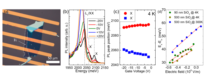
As discussed in the main text, we observe a clear dependence of the exciton-trion peak separation on the applied gate voltage in our samples due to a change of the Fermi energy Mak et al. (2013). The results presented in the manuscript are confirmed by measurements on a second sample, in which a p-doped Si chip with 90 nm SiO2 thermal oxide and prestructured Ti:Au stripes on top serves as the final substrate for our transfer process. Fig. 5(a) shows a microscope image of this sample. We use the Si as the backgate and observe a very similar behavior as discussed in the main text (see Fig. 5(b) and (c)). The X peak experiences a reduction of its intensity and a blueshift with increasing gate voltage, whereas the X- peak undergoes a redshift and an increase of its intensity. For positive gate voltages, the X- feature merges with the L1 peak. By taking into account the oxide thickness and the dielectric constant of SiO2, we get a measure for the electric field in our structures. Thus, we can directly compare samples with 90 nm and 500 nm SiO2. Fig. 5(d) highlights the peak separation energy of exciton and trion, , as a function of the applied electric field for different samples and temperatures. The data exhibits the expected linear correlation, as indicated by the linear fits. Both sample structures show a very similar behavior in PL measurements at 4 K, with a nearly identical linear slope. The vertical offset between the measurements on the samples indicates that the two contacted WS2 flakes have different residual doping. The most likely cause for the vertical offset in the measurements on the sample with 500 nm SiO2 layer at different temperatures is the sample environment: the room-temperature measurement was performed with the sample in air, while low-temperature measurements were performed with the sample in vacuum. Surface adsorbates may accumulate on top of a flake under ambient conditions and shift the Fermi level. The minimum peak separation between exciton and trion that we observe in gate-dependent measurements is 30 meV, which is an upper boundary for the trion binding energy.