Effect of Low-Damage Inductively Coupled Plasma on Shallow NV Centers in Diamond
Abstract
Near-surface nitrogen-vacancy (NV) centers in diamond have been successfully employed as atomic-sized magnetic field sensors for external spins over the last years. A key challenge is still to develop a method to bring NV centers at nanometer proximity to the diamond surface while preserving their optical and spin properties. To that aim we present a method of controlled diamond etching with nanometric precision using an oxygen inductively coupled plasma (ICP) process. Importantly, no traces of plasma-induced damages to the etched surface could be detected by X-ray photoelectron spectroscopy (XPS) and confocal photoluminescence microscopy techniques. In addition, by profiling the depth of NV centers created by keV of nitrogen implantation energy, no plasma-induced quenching in their fluorescence could be observed. Moreover, the developed etching process allowed even the channeling tail in their depth distribution to be resolved. Furthermore, treating a 12C isotopically purified diamond revealed a threefold increase in T2 times for NV centers with nm of depth (measured by NMR signal from protons at the diamond surface) in comparison to the initial oxygen-terminated surface.
The negatively-charged nitrogen-vacancy (NV) center in diamond has attracted increasing attention due to its outstanding properties. It is an atomic-sized, bright and stable single photon sourceJelezko and Wrachtrup (2006) with relatively long coherence times, ranging milliseconds in isotopically purified single crystal diamond layersJahnke et al. (2012); Balasubramanian et al. (2009). Additionally, its electron spin can be coherently manipulated by microwave and readout optically at room temperature. In the recent years the use of near-surface (shallow) NV centers as sensors to detect external nuclearStaudacher et al. (2013); Mamin et al. (2013); Müller et al. (2014) and electronicGrotz et al. (2011); Shi et al. (2015) spins have been successfully demonstrated. However, since the signal detection relies on the relatively weak dipolar coupling to the targeted external spins, decaying proportional to r-3 (with being the distance between the targeted and sensor spins), NV centers must be located close to the diamond surface ( nm)Staudacher et al. (2013); Mamin et al. (2013).
Up to now, the engineering of near-surface NV centers has relied mostly on low-energy nitrogen implantationPezzagna et al. (2010) or epitaxial growth of high quality nitrogen-doped CVD diamond followed by electronOhno et al. (2012) or ion irradiationOhno et al. (2014). Furthermore, NV centers can be brought closer to the diamond surface by post-treatments such as thermal oxidationLoretz et al. (2014); Kim et al. (2014) and etching in plasmaKim et al. (2014); Santori et al. (2009); Cui et al. (2015).
A major drawback for thermal oxidation is the uncertainty in the resulting etching rate and infeasibility of selective etching. Overcoming these issues, plasma processes are widely employed, providing a smooth and uniform method to selectively etch diamond. In particular for reactive ion etching (RIE) processes, the presence of a bias between the plasma source and the sample leads to ion bombardment on the diamond surface. This results in an enhanced etching rate and directionality of the process, but also produces a highly damaged layer containing vacancies and implanted ions of a few nanometers below the diamond surfaceKawabata et al. (1988). If located in the vicinity of NV centers, these defects can lead to suppression of the photoluminescence emission and degraded spin propertiesKim et al. (2014); Cui et al. (2015). Thus a precise, uniform and high-selective etching process, by which the damages to the etched diamond surface are avoided, is highly desired. To that aim we present a low-pressure oxygen inductively coupled plasma (ICP) process with nanometric etching precision and high reproducibility. All reported plasma-related processes were performed in an Oxford PlasmaPro NGP80 machine equipped with an additional ICP source (Oxford Plasma Technologies). The effect of the developed etching process in the optical and spin properties of near-surface NV centers in diamond CVD layers will be explored in details.
The optimized plasma recipe consists of two steps: first the RIE source with mTorr constant chamber pressure and W of power is used to ignite the plasma for a few seconds. Afterward the RIE source is switched off and the plasma is sustained only by the ICP source, which is located at a remote position from the substrate holder in the chamber. Under such conditions the sample surface is exposed mainly to neutral chemical radicals. This is supported by the fact that using both sources simultaneously showed no significant change in the DC bias, while varying the ICP power up to W and keeping the RIE power constant at W. This plasma process will be referred further as “oxygen soft plasma” in this paper.
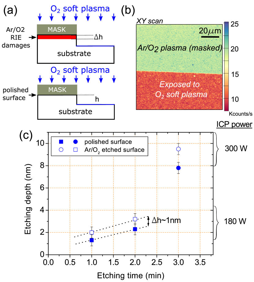
A high-purity single-crystal -oriented electronic grade CVD diamond with an as-polished surface was taken as a substrate. The initial root mean squared (RMS) surface roughness was measured to be in the range of 1 nm by atomic force microscopy (AFM), allowing a detailed analysis in the quality of the post-treated surface. A schematic representation of the experiment is presented in figure 1(a). The sample was masked by lithography-patterned AZ E (MicroChemicals) photoresist to protect part of the polished surface. Subsequently, the sample was exposed to Ar/O2 RIE plasma for 16 minutes ( sccm and sccm respectively, mTorr chamber pressure and W RIE power). Next, the polished and the Ar/O2 RIE etched regions were again patterned by optical lithography, leaving stripes exposed to the subsequent treatment with the oxygen soft plasma. Such procedure yields four different areas on the diamond surface, namely (I.) as-polished, (II.) polished combined with the oxygen soft plasma, (III.) Ar/O2 RIE as-etched and (IV.) Ar/O2 RIE etched combined with the oxygen soft plasma. The sample was cleaned by boiling in a triacid mixture of H2SO4:HNO3:HClO4, :: volumetric ratio for three hours, referred as wet chemical oxidation (WCO).
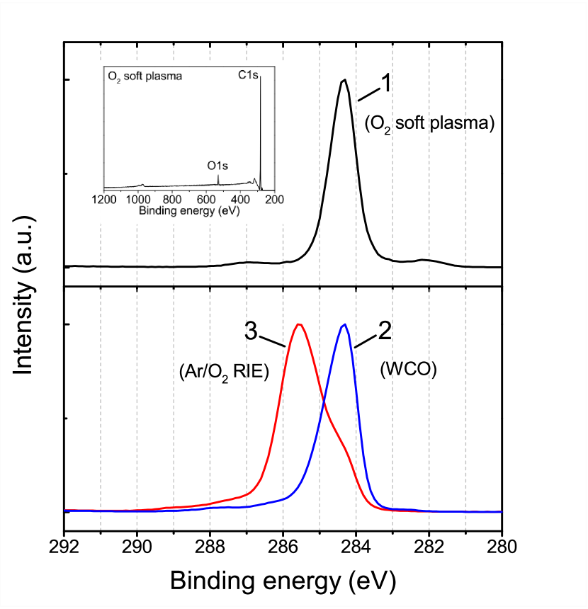
To analyze the effect of the oxygen soft plasma in the properties of the described surface areas, confocal photoluminescence (PL) microscopy (home-build setup with a nm wavelength excitation laser), AFM and X-ray photoelectron spectroscopy (XPS) measurements were performed. The XPS photoemmision spectra were acquired using a AXIS ULTRA (Kratos Analytical Ltd.) spectrometer equipped with a monochromatized Al K (1486.6 eV) radiation source. The binding energy scale was calibrated by means of Ag and Au reference samples. High resolution spectra of the Cs core levels detected normal to the sample surface are shown in figure 2. There, the spectrum after the oxygen soft plasma (curve 1) is compared to those from a reference diamond sample. The spectral lines related to WCO and the previously described Ar/O2 RIE plasma process are shown in curves 2 and 3, respectively.
The Ar/O2 RIE treatment has been reported to induce detectable damages to the diamond sub-surface layersDenisenko et al. (2010). In the presented confocal PL microscopy measurement (figure 1(b)), these damages are revealed as a slightly increased luminescence background. The lower part of this PL scan had an additional oxygen soft plasma treatment for 1 minute with W of ICP power. As it can be seen, this post-treatment was enough to eliminate the background related to the Ar/O2 RIE process, showing a clear fluorescence contrast. Furthermore, related AFM measurements are presented in figure 1 (c). Threating the as-polished and the previously Ar/O2 RIE etched regions simultaneously with the oxygen soft plasma, approximately nm more in the etching depth (represented by h) could be observed in the Ar/O2 RIE etched region. Longer exposure times and also different ICP powers did not show significant increase in this difference. This is attributed to the faster initial removal of the RIE-damaged diamond layers. In addition, the corresponding XPS spectrum to the Ar/O2 RIE plasma process is presented in figure 2, curve 3. It shows a broad peak shifted by approximately eV with respect to the sp3 bulk component at eV. This is associated to an amorphous phase of carbon (-sp3) of a few nanometers in thicknessKawabata et al. (1988). Importantly, such signature for RIE-induced damages is absent in the C1s core level spectrum from the surface treated with the oxygen soft plasma process, as presented in figure 2, curve 1. Hereafter, the results by confocal PL microscopy, AFM and XPS techniques indicates the complete removal of the amorphous RIE-damaged diamond sub-surface layers by the oxygen soft plasma. Moreover, the extracted thickness of nm is in good agreement with the literatureKawabata et al. (1988).
Besides, the spectrum showed in figure 2, curve 1 is shown to be very similar to the one related to WCO (curve 2). The dominance of the sp3 bulk component is observed together with small peaks shifted to higher binding energies, known to be related to carbon-oxygen functional groups on the diamond surfaceYagi et al. (1999). Both oxygen soft plasma- and WCO-treatments show similar intensities of the Os core level spectra (see the inset in figure 2), indicating a full coverage of the surface with oxygen species.
In addition to that, it is also known that new NV centers are formed by post-plasma high temperature annealingKim et al. (2014). In contrast to the surface treated with the Ar/O2 RIE plasma process, this effect was not observed in the present experiment with an additional oxygen soft plasma treatment before the annealing procedure. This supports further the previously mentioned results, confirming the removal of the sub-surfaces defective layers that would contain plasma-induced vacancies.
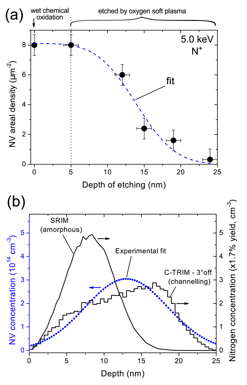
Near-surface NV centers can be exquisite tools to detect plasma-induced defects since they are extremely sensitive to surface modificationsKim et al. (2014); Cui et al. (2015); Santori et al. (2009). Therefore, to validate the oxygen soft plasma process, the depth profile of NV centers created close to the diamond surface by keV of nitrogen implantation energy with a dose of cm-2 was analyzed. After the implantation the sample was consequently submitted to high temperature annealing at approximately C in high vacuum ( mbar) for two hours and the mentioned WCO treatment. The chosen annealing temperature is known to minimize the density of paramagnetic defects such as vacancy complexesYamamoto et al. (2013).
The evaluation consisted of sequential etching steps using the oxygen soft plasma process followed by confocal PL microscopy measurements to extract the areal density of NV centers. Each etching step comprised 1 minute of RIE plasma - aiming low etching rate and homogeneity - followed by 1 minute of the ICP with W power - aiming the removal of the RIE-induced surface damages (steps referred to the oxygen soft plasma recipe). The experimental areal density of NV centers versus the etching depth is plotted in figure 3(a). For simplicity, the experimental data was fitted to a Gaussian complementary error function. In figure 3(b) the experimentally fitted profile is compared to SRIMZiegler et al. and CTRIMPosselt and Biersack (1992) simulations, which consider an amorphous material and ion channeling in a crystalline lattice, respectively. A good agreement was found to the CTRIM simulated profile for a -oriented diamond surface with a -off implantation angle, which is in the frame of the accuracy specified for surface polishing and the accuracy of the implantation process. Thus, the presence of ion channeling could be resolved even for a low energy of implantation, as also predicted by theoretical investigations using molecular dynamics simulationsAntonov et al. (2014). Besides, the yield (conversion from implanted nitrogen atoms to NV centers) was found to be , a typical value for the used energy of implantationPezzagna et al. (2010). It should be highlighted that the point related to the first etching step at nm (vertical doted line in figure 3(a)) does not show rapid quenching in the density of NV centers in comparison to the initial value (WCO). This contrasts to other plasma etching processes reported in literatureKim et al. (2014); Cui et al. (2015). Thereby one could ascertain that the developed process preserves the optical properties of shallow NV centers.
The influence of the oxygen soft plasma on the spin coherence characteristics (T2) of shallow NV centers is of great importance and will be discussed below. To avoid any undesired effects due to polishing-induced defectsVolpe et al. (2009) or 13C spin bath noiseMarkham et al. (2011), this study was conducted on an as-grown surface of a 12C isotopically purified () diamond CVD layer with more than m in thickness, overgrown on a natural abundance, single-crystal -oriented electronic grade CVD diamond substrate (Element Six).
The sample was first implanted with nitrogen ions at keV of energy with a dose of cm-2 followed by high temperature annealing and WCO as described before. Single NV centers were addressed by confocal microscopy technique. Coherence times were measured by means of optically detected magnetic resonance (ODMR) method using a Hahn echo sequence scheme, which allows us to probe the coherence between the ground state (bright state) and (dark state) of the NV center electronic spin. A magnetic field of approximately Gauss was aligned parallel to the NV axis. Further on, nuclear magnetic resonance (NMR) signal originating from protons present in the immersion oil on the diamond surface was used to calibrate the depth of individual NV centers by means of a XY sequence scheme, as described in reference Staudacher et al. (2013). The related results are summarized in figure 4.
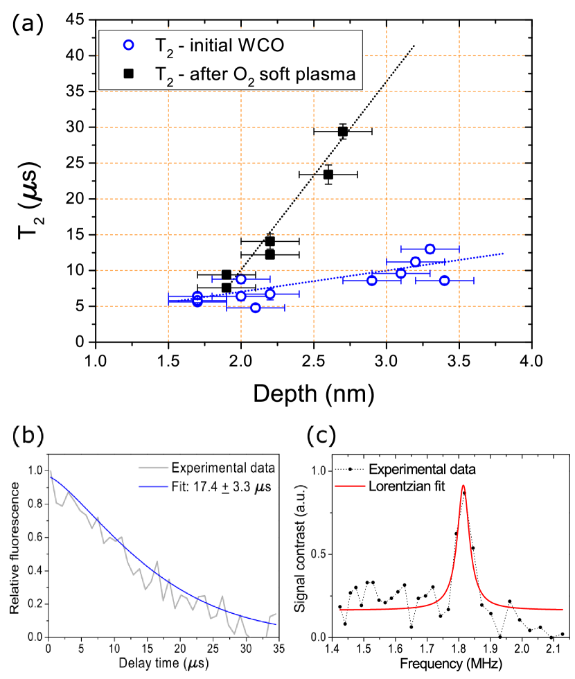
After treating the initial surface with the oxygen soft plasma process for minutes with W of ICP power (corresponding to nm of etching depth), NV centers located a few nanometers ( nm) from the diamond surface could still be observed (figure 4(a)). This supports further the assumption of preservation of the optical properties of shallow NV centers. Likewise, the values of coherence times showed an improvement up to times, yielding an NMR signal up to T, especially for NV centers located nm below the surface. The reason for such improvement is not clear yet, but it can be associated to modifications of the electronic configuration of the diamond surface, which would be affected now by the oxygen soft plasma. Indeed, fluctuations of surface charges are believed to be a significant source of decoherence due to electric field noiseKim et al. (2015), meaning that the developed oxygen soft plasma process may increase the surface charge stability. Further studies must be performed to mitigate this effect.
To summarize, an alternative method for etching diamond using an oxygen ICP process was presented. Possessing qualities such as nanometric-precise etching rate, high reproducibility and selective etching, this plasma process was demonstrated to be a promising technique to bring NV centers closer to the diamond surface while preserving their optical and spin characteristics. The presented technique could be used in the future to precisely control the depth of created NV centers by a variety of techniques such as ion and electron irradiation. In addition, being able to profile the depth distribution of NV centers with such precision, one would gain important information about the vacancy diffusion process regarding the creation of color centers in diamond.
F. F. de Oliveira acknowledges the financial support by CNPq project number . J. W. acknowledges the support by the EU via ERC grant SQUTEC and IP DIADEMS as well as the DFG.
References
- Jelezko and Wrachtrup (2006) F. Jelezko and J. Wrachtrup, phys. stat. sol. (a) 203, 3207 (2006).
- Jahnke et al. (2012) K. D. Jahnke, B. Naydenov, T. Teraji, S. Koizumi, T. Umeda, J. Isoya, and F. Jelezko, Applied Physics Letters 101, 012405 (2012).
- Balasubramanian et al. (2009) G. Balasubramanian, P. Neumann, D. Twitchen, M. Markham, R. Kolesov, N. Mizuochi, J. Isoya, J. Achard, J. Beck, J. Tissler, V. Jacques, P. R. Hemmer, F. Jelezko, and J. Wrachtrup, Nature Materials 8, 383 (2009).
- Staudacher et al. (2013) T. Staudacher, F. Shi, S. Pezzagna, J. Meijer, J. Du, C. A. Meriles, F. Reinhard, and J. Wrachtrup, Science 339, 561 (2013).
- Mamin et al. (2013) H. J. Mamin, M. Kim, M. H. Sherwood, C. T. Rettner, K. Ohno, D. D. Awschalom, and D. Rugar, Science 339, 557 (2013).
- Müller et al. (2014) C. Müller, X. Kong, J.-M. Cai, K. Melentijevic, A. Stacey, M. Markham, D. Twitchen, J. Isoya, S. Pezzagna, J. Meijer, J. F. Du, M. B. Plenio, B. Naydenov, L. P. McGuinness, and F. Jelezko, Nature Communications 5 (2014), 10.1038/ncomms5703.
- Grotz et al. (2011) B. Grotz, J. Beck, P. Neumann, B. Naydenov, R. Reuter, F. Reinhard, F. Jelezko, J. Wrachtrup, D. Schweinfurth, B. Sarkar, and P. Hemmer, New Journal of Physics 13 (2011), 10.1088/1367-2630/13/5/055004.
- Shi et al. (2015) F. Shi, Q. Zhang, P. Wang, H. Sun, J. Wang, X. Rong, M. Chen, C. Ju, F. Reinhard, H. Chen, J. Wrachtrup, J. Wang, and J. Du, Science 347, 1135 (2015).
- Pezzagna et al. (2010) S. Pezzagna, B. Naydenov, F. Jelezko, J. Wrachtrup, and J. Meijer, New Journal of Physics 12, 065017 (2010).
- Ohno et al. (2012) K. Ohno, F. Joseph Heremans, L. C. Bassett, B. A. Myers, D. M. Toyli, A. C. Bleszynski Jayich, C. J. Palmstrøm, and D. D. Awschalom, Applied Physics Letters 101, 082413 (2012).
- Ohno et al. (2014) K. Ohno, F. Joseph Heremans, C. F. de las Casas, B. A. Myers, B. J. Alemán, A. C. Bleszynski Jayich, and D. D. Awschalom, Applied Physics Letters 105, 052406 (2014), 10.1063/1.4890613.
- Loretz et al. (2014) M. Loretz, S. Pezzagna, J. Meijer, and C. L. Degen, Applied Physics Letters 104, 033102 (2014).
- Kim et al. (2014) M. Kim, H. J. Mamin, M. H. Sherwood, C. T. Rettner, J. Frommer, and D. Rugar, Applied Physics Letters 105, 042406 (2014).
- Santori et al. (2009) C. Santori, P. E. Barclay, K.-M. C. Fu, and R. G. Beausoleil, Physical Review B 79, 125313 (2009).
- Cui et al. (2015) S. Cui, A. S. Greenspon, K. Ohno, B. A. Myers, A. C. B. Jayich, D. D. Awschalom, and E. L. Hu, Nano Letters 15(5), 2887 (2015).
- Kawabata et al. (1988) Y. Kawabata, J. Taniguchi, and I. Miyamoto, Diamond and Related Materials 13, 93 (1988).
- Denisenko et al. (2010) A. Denisenko, A. Romanyuk, C. Pietzka, J. Scharpf, and E. Kohn, Journal of Applied Physics 108, 074901 (2010).
- Yagi et al. (1999) I. Yagi, H. Notsu, T. Kondo, D. A. Tryk, and A. Fujishima, Journal of Electroanalytical Chemistry 473, 173 (1999).
- Yamamoto et al. (2013) T. Yamamoto, T. Umeda, K. Watanabe, S. Onoda, M. L. Markham, D. J. Twitchen, B. Naydenov, L. P. McGuinness, T. Teraji, S. Koizumi, F. Dolde, H. Fedder, J. Honert, J. Wrachtrup, T. Ohshima, F. Jelezko, and J. Isoya, Physical Review B 88, 075206 (2013).
- (20) J. F. Ziegler, J. P. Biersack, and M. D. Ziegler, “Srim, the stopping and range of ions in matter,” .
- Posselt and Biersack (1992) M. Posselt and J. P. Biersack, Nucl. Instr. Meth. Phys. Res. Sec. B 64, 706 (1992).
- Antonov et al. (2014) D. Antonov, T. Häußermann, A. Aird, J. Roth, H.-R. Trebin, C. Müller, L. McGuinness, F. Jelezko, T. Yamamoto, J. Isoya, S. Pezzagna, J. Meijer, and J. Wrachtrup, Applied Physics Letters 104, 012105 (2014).
- Volpe et al. (2009) P.-N. Volpe, P. Muret, F. Omnes, J. Achard, F. Silva, O. Brinza, and A. Gicquel, Diamond and Related Materials 18, 1205 (2009).
- Markham et al. (2011) M. Markham, J. Dodson, G. Scarsbrook, D. Twitchen, G. Balasubramanian, F. Jelezko, and J. Wrachtrup, Diamond and Related Materials 20, 134 (2011).
- Kim et al. (2015) M. Kim, H. J. Mamin, M. H. Sherwood, K. Ohno, D. D. Awschalom, and D. Rugar, ArXiv e-prints (2015), arXiv:1506.00295 [cond-mat.mes-hall] .