Low Operation Voltage Ferroelectric Field-Effect Transistor Based on Polarization Rotation Effect
Abstract
The effect of polarization rotation on the performance of metal oxide semiconductor field-effect transistors was investigated with a Landau-Ginzburg-Devonshire theory based model. In this analytical model, depolarization field, polarization rotations and the electrostatic properties of the doped silicon substrate are considered to illustrate the size effect of ferroelectric oxides and the stability of polarization in each direction. Based on this model, we demonstrate that MOSFET operation could be achieved by polarization reorientation with a low operating voltage, if the thickness of ferroelectric oxide is properly selected. Polarization reorientation can boost the surface potential of the silicon substrate, leading to a subthreshold swing lower than 60 mV/decade. We believe that this model could provide guidance in designing electronic logic devices with low operating voltages and low active energy consumption.
pacs:
Valid PACS appear hereI Introduction
Ferroelectric oxides are a promising class of materials for application in electronic devices due to their intrinsic spontaneous electric polarization, which can not only control the conductance of the channel, but also can be reoriented by an external electric field Mathews et al. (1997); Naber et al. (2005); Hoffman et al. (2010); Fu and Cohen (2000). By modulating the polarization of ferroelectric oxides, programmable binary logic devices can be achieved, and the fast reorientation of polarization enables fast switching and lower–power operation of the metal–oxide–semiconductor field–effect transistor (MOSFET) Kimura et al. (2004); Liu et al. (2013).
Here, we aim to provide guidance about designing a programmable fast switching MOSFET with proper size, by considering factors which were rarely included in previous modeling, but may strongly affect the polarization reorientation and size effect of ferroelectric oxides. Many analytical models based on the Landau-Ginzburg-Devonshire (LGD) theory have been proposed previously Chen et al. (2012, 2011) to simulate the electrical behaviors of MOSFETs. These models provide an insightful understanding about the mechanisms of ferroelectric oxide based MOSFETs and guide the fabrication of novel devices. However, there are still several vital factors beyond the scope of previous models. First, the effect of the polarization distribution in three dimensions (3D) on the channel current–gate voltage relationship of a MOSFET was rarely considered, even though there were a lot of studies about polarization in 3D and its response to electric fields in different orientations Bellaiche et al. (2001); Hlinka and Márton (2006); Fu and Cohen (2000); Nagarajan et al. (2002). For simplicity, the polarization of the ferroelectric oxide in a MOSFET is usually treated in one dimension. It is true that the channel conductance is mainly modulated by the out–of–plane polarization, but it is also important to note that the polarization components in all three dimensions are coupled together, and the in–plane polarization strongly influences the electric susceptibility out of plane. The second factor is the electrostatic properties of the channel and gate electrode. It is widely known that the distribution of charge in electrodes, which is parameterized as screening length, determines the strength of depolarization field, which affects the magnitude of the spontaneous ferroelectric polarization Batra et al. (1973); Sai et al. (2005); Al-Saidi and Rappe (2010); MendezPolanco et al. (2012).
In this letter, we propose a LGD theory based single crystal model with detailed analysis of these factors, in order to provide strategies for designing a low operation voltage ferroelectric field-effect transistor Datta et al. (2013); Salahuddin and Datta (2008). A previous study argues that a subthreshold swing lower than 60 mV/decade can be achieved by the negative capacitance effect Salahuddin and Datta (2008), but there is also debate that direct current negative capacitance is not possible, due to Gibbs free energy considerations Krowne et al. (2011). In our model, the polarization dynamics obeys the Landau–Khalatnikov equation and is always minimizing the Gibbs free energy under a unidirectional gate voltage. We demonstrate that fast switching (subthreshold swing lower than 60 mV/decade) can be achieved by a proper design of the ferroelectric oxide size. The mechanism is that during the process of polarization reorientation, the tendency to possess spontaneous polarization in a new direction boosts the screening charge accumulation and channel current increases, leading to a low subthreshold swing.
II Model Approach
The LGD model is a phenomenological theory which describes the electrical properties of ferroelectric oxides. In this model, the thermodynamic potential (Gibbs free energy ) of a single crystal ferroelectric oxide is given as a function of polarization in three directions Pertsev et al. (1998); Koukhar et al. (2001).
| (1) | ||||
Taking external electric field and internal depolarization field into consideration, electrostatic terms should be added as
| (2) |
FIG. 1. shows the schematic of the MOSFET that we study. The insulator between the gate electrode and doped silicon substrate is a ferroelectric oxide Salahuddin and Datta (2008); Ngo et al. (2014). The axis is normal to the ferroelectric oxide/silicon interface. In the and directions, there is no external voltage, and short circuit conditions are applied Batra et al. (1973); Mehta et al. (1973); Kolpak et al. (2006).
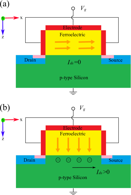
For the case that a gate voltage is imposed on the MOSFET, we have the following equations:
| (3) |
and are the voltage drop across the electrode and the ferroelectric oxide in the , and directions. is the surface potential of the silicon substrate, and it can also be viewed as the voltage drop in the doped silicon substrate. The flat band potential , which results from the alignment of the Fermi levels of the gate electrode, oxide, and silicon substrate is included in . The electric field is determined by both the external applied voltage and the electrostatic properties of the ferroelectric oxide and electrodes Wurfel and Batra (1973); Junquera and Ghosez (2003); Kim et al. (2005). It is widely accepted that the charge density in noble metal electrodes follows the Thomas-Fermi distribution, and this distribution causes a voltage drop across the electrodes. The following derivation calculating this potential drop follows the main idea in Ref. Mehta et al. (1973), but is re-interpreted. Taking the direction as an example and the electrostatic properties in the , directions following similar rules, the relationship between the electric field and the charge density takes the form
| (4) |
, and are the electric field, the charge density and the electron density in electrodes at the position . is the average electron density in a neutral electrode. is the electronic charge. and are the electric permittivities of the vacuum and electrode. Meanwhile, the potential drop is expressed as
| (5) |
The electrons in metal electrodes are treated as a free Fermi gas, so the local potential and the electron density are related as
| (6) |
| (7) |
is the reduced Planck constant and is the electronic mass. By combining equations (5) and (6), we have
| (8) |
Taking the derivative of equation (4), we have
| (9) |
The characteristic length , which is also called screening length and determines the dispersion of electrons in electrodes, is defined as
| (10) |
Therefore, equation (9) is rewritten as
| (11) |
The boundary conditions are
| (12) |
is the screening charge density at the ferroelectric/oxide electrode interface, which is also . Thus, the electric field and potential drop through one electrode are
| (13) |
| (14) |
The heterostructure of electrode, ferroelectric oxide, and silicon substrate can be regarded as a capacitor, with equal charge densities at each interface. However, the charge distribution in the doped silicon substrate is quite different from that in metal. This is because electrons in the metal are treated as a free electron gas. This is the basic approximation of the Thomas-Fermi model. But doped silicon is a semiconductor, and the free carrier density is local potential dependent Sze and Ng (2006); Taur et al. (1998). The interface charge density-potential relationship in the silicon substrate is given by
| (15) |
| (16) |
is the surface potential of the silicon substrate. is the Boltzmann constant. Other parameters are listed and described in TABLE .
From the analysis above, we see that the charge density decreases gradually away from the oxide in both the metal electrode and the doped silicon substrate, even though the analytical expressions and physical mechanisms which govern the charge distribution are different. As a result, there are voltage drops through each layer. These voltage drops could counteract or completely neutralize the applied gate voltage, exerting significant influence on the magnitudes of ferroelectric polarization and charge in the channel. Equation demonstrates that there is a one-to-one correlation between the interface charge density and the surface potential . is a function of :
| (17) |
The voltage drop across the ferroelectric oxide takes the form
| (18) |
is the thickness of the ferroelectric film and is the polarization in the direction. With the analysis above, equation set is rewritten as
| (19) |
For short-circuit conditions, in order to balance the potential drop in the electrodes, the sign of should be opposite to that of . This indicates that surface charge density should be smaller than polarization, which means an incomplete screening of the polarization charge. As a result, an electric field (depolarization field) is induced opposite to the polarization. The potential drop in the metal electrodes, which is proportional to screening length, is the origin of the incomplete polarization charge screening and the depolarization field which suppresses ferroelectricity.
The energy surface versus polarization direction and magnitude can be plotted under the electrostatic restrictions expressed in equation . After acquiring the energy surface, polarization dynamics on the energy surface is simulated by the Landau–Khalatnikov equation Landau and Khalatnikov (1954); Lo (2003); Zhang and Bhattacharya (2005),
| (20) |
is the polarization dynamic parameter. is the thermodynamic potential defined in equation (2) with the restriction shown in equation (19). The most stable polarization is the one which minimizes Gibbs free energy . However, if the polarization is not in a local minimum, it cannot move to one instantaneously. The rate of return to a minimum is determined by many factors. For example, the resistance of the circuits affects this rate, because polarization evolution must be accompanied by screening charge transmission. The polarization dynamic parameter is related to the mobility of polarization, as can be regarded as the driving force of polarization and is the speed of polarization evolution. The applied time–varying gate voltage takes the form,
| (21) |
Here, we do not mean that the applied gate voltage is oscillatory. Instead, we are simulating one on/off programmable cycle , and the increase/decrease of the gate voltage takes the sine form. Equation (20) is rewritten as
| (22) |
is the effective polarization dynamic parameter. and can be calculated from and the drain-source current is obtained by the Pao-Sah double integral Pao and Sah (1966).
| (23) |
where the parameters in this simulation are listed in TABLE , and the function is given in Ref. Taur et al. (1998).
| Description | Value | |
|---|---|---|
| Temperature | 298 K | |
| Coefficient in LGD theorya | m/F | |
| Coefficient in LGD theorya | m5/C2F | |
| Coefficient in LGD theorya | m5/C2F | |
| Coefficient in LGD theorya | m9/C4F | |
| Coefficient in LGD theorya | m9/C4F | |
| Coefficient in LGD theorya | m9/C4F | |
| Screening lengths in noble metalb | 0.04 nm | |
| Dielectric constant of noble metalb | 2.0 | |
| Substrate doping concentrationc | cm-3 | |
| Intrinsic carrier concentrationc | cm-3 | |
| Dielectric constant of silicon | 11.7 F/m | |
| Effective electron mobility | m2/Vs | |
| Width of the silicon channel | m | |
| Length of the silicon channel | m | |
| Equals to |
III Results and Analysis
The ferroelectric oxide we choose is BaTiO3, which possesses a relatively large spontaneous polarization ( C/m2) at room temperature Al-Saidi and Rappe (2010).
In order to simulate the energy surface, we vary the surface potential and polarization . For each , charge density and polarization are determined uniquely by equations and . At room temperature, the BaTiO3 crystal has a tetragonal phase. The polarization orients either out of plane or in plane. We set the in–plane polarization direction as the direction and . Here, we should also note that we assume that the in–plane polarization has no effect on the channel. Therefore, it is not necessary that the source channel–drain–current flows along the direction. Electric field is obtained by the electrostatic restrictions in equation . Then energy surfaces describing Gibbs free energy with respect to and are calculated by formula and .
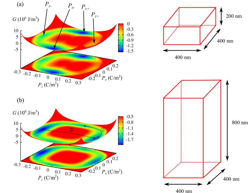
In FIG. 2, we have plotted two energy surfaces of BaTiO3 with different thicknesses in the and directions on a p–type silicon substrate.
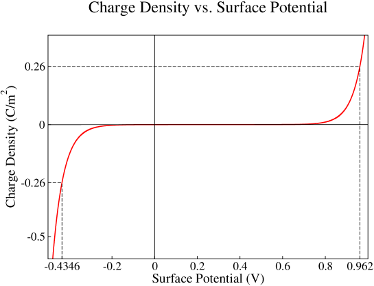
From the graphs, we can see that for out–of–plane polarization, a negative orientation (pointing to gate electrode, with negative ends of oxide dipoles toward the channel) is more favorable when there is no applied voltage. This is because for a p–type silicon substrate, positive screening charge is more likely to accumulate at the interface, leading to the polarization pointing away from the substrate/ferroelectric oxide interface. FIG. 3 shows the relationship of the surface potential and the interface charge density in the p–type silicon substrate. A positive (pointing to silicon substrate) spontaneous polarization C/m2 corresponds to a surface potential eV, while C/m2 corresponds to a surface potential eV. The depolarization fields through the ferroelectric oxide are calculated with the equation (19):
| (24) |
| (25) |
The depolarization field for positive polarization is larger, and this explains why on the energy surface with no gate voltage, a negative polarization is more favorable than a positive one.
Besides, the graphs also demonstrate the known relation that the thicker the ferroelectric oxide is in one direction, the more stable the polarization in this direction. As shown in equation , if the thickness overwhelms the screening length, the potential drop in the electrodes can be neglected Spanier et al. (2006). As a result, the electric field through the ferroelectric oxide decreases, making the polarization in this direction more favorable.
These results also illustrate that we can modulate the global minimum by adjusting the three-dimensional size of the ferroelectric oxide. An energy surface we are particularly interested in possesses the global minimum for . When the gate voltage is applied, the local minimum corresponding to becomes deeper and polarization rotates to the direction. After the gate voltage is turned off, the polarization relaxes back along the direction. Meanwhile, the depth of the local minimum for is close to that for . In such a situation, a relatively small applied gate voltage could induce polarization to rotate from the direction to the direction. The channel current strongly depends on the interface charge density, which is approximately equal to the polarization in the direction.
| (26) |
Here, we provide guidance about how to select the optimal widths of the ferroelectric oxide, in order to make the polarization rotation likely to occur. First, in order to make the polarization orient in the direction without gate voltage, the depolarization field for should be smaller than the one that corresponds to ,
| (27) |
Typically, the dielectric constant and screening length of the noble metal electrodes are and 0.4 Å Kim et al. (2005). For these values, we have the criterion
| (28) |
In order to have a programmable device, when the applied gate voltage returns 0, the polarization should spontaneously return from the position to the minimum for on the energy surface. According to the Landau–Khalatnikov equation, the position on the energy surface should be a saddle point,
| (29) |
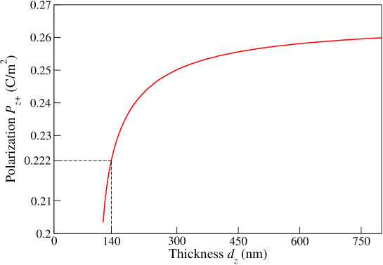
The value of increases with thickness in the direction, since a thinner film means a larger depolarization field which suppresses the ferroelectricity. The relationship is shown FIG. 4.
| (30) |
Therefore nm is a necessary condition for the polarization rotating back to the direction.
| (31) |
According to the analysis above, in this study, the BaTiO3 dimensions are selected as nm and nm.
Hysteresis loops with different values of are calculated and shown in FIG. 5.
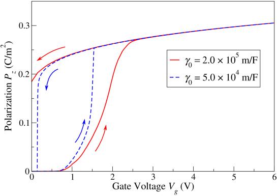
It demonstrates that if is too large, the out–of–plane polarization cannot reduce to 0 and the device is not ready for the next program cycle. From our simulation, the threshold for out–of–plane polarization returning to 0 completely is around m/F. is not only frequency dependent as shown in equation (22), but also dependent on the resistance in the circuit Sivasubramanian et al. (2003); Zhou et al. (2005), since polarization dynamics is accompanied by screening charge transmission Kim et al. (2005); Kalinin et al. (2002). Therefore, in order to make in the acceptable range and to have a short switching time, the resistance in the circuit should be low.
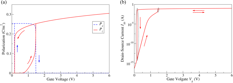
To evaluate the performance of MOSFET, The drain–source current and gate voltage relationship is calculated based on Pao–Sah double integral. The simulated hysteresis loop and curve for m/F are shown in FIG. 6 (b).
From the simulation, it can be seen that the on/off ratio of the channel current is large, which means that this device is extremely suitable for logic technology. This large on/off ratio results from spontaneous polarization rotation, because the spontaneous polarization attracts screening charge as free carriers, leading to a large on–current. The segments in the curve circled by dashed lines possess subthreshold swings lower than 60 mV/decade. For the segment with and increasing, mV/decade, and the of the decreasing segment is even lower. This is because, as the gate voltage increases and exceeds the threshold voltage, the polarization rotates and boosts free carriers in the silicon channel, inducing a steep increase of the channel current. From FIG. 6, we can see that the steep change of the channel current is accompanied by polarization reorientation.
can be expressed as Salahuddin and Datta (2008)
| (32) |
During the polarization reorientation period, the polarization changes suddenly from an in–plane one corresponding to zero surface potential to a positive out–of–plane polarization, which maintains a large surface potential as demonstrated in FIG. 3. The surface potential is boosted as
| (33) |
causing to break the 60 mV/decade limit.
Compared with polarization inversion, polarization rotation possesses many advantages for electronic device applications. First, as shown in FIG. 2, in the polarization rotation process, a much lower energy barrier is overcome, leading to a lower polarization rotation voltageQi et al. (2009); Secondly, the working state of the MOSFET can be modulated by a unidirectional gate voltage. This simulation and the guidance about designing the ferroelectric oxide size can be also extended to other types of channel, such as quantum well and graphene Liu et al. (2013); Ali et al. (2011); Baeumer et al. (2015); Hong et al. (2009, 2010). The only part that needs to be modified according to the electric properties of new channels is the surface potential–interface charge density relationship
| (34) |
In the simulation, the focus is BaTiO3, but this analytical model can also be applied to other ferroelectric oxides, such as PbTiO3 and PbZr1-xTixO3. PbTiO3 possesses a larger energy barrier in the polarization process compared with BaTiO3 Cohen (1992). Therefore, a larger applied gate voltage is needed or we should use PbTiO3 with smaller dimensions. Also, a single–domain ferroelectric oxide is assumed in this model. However, the effect is not limited to a single crystal. When a gate voltage is applied, polarization in the direction increases in different grains and finally the polarization becomes approximately uniform. After the voltage is removed, the polarization relaxes back to the plane. Multiple domains may form in each grain, but the polarization distribution in plane has little effect on the channel conductance.
IV Conclusion
In summary, the polarization distribution in 3D and the electrical properties of the electrodes and the silicon substrate were highlighted in this LGD–theory–based model. Our model demonstrated that polarization reorientation can modulate the drain–source current effectively. Besides, the choice of electrodes and the dimensions of the ferroelectric oxide are key factors in determining the performance of a MOSFET with depolarization fields. With proper selection of the thicknesses, field effect transistor with low operating voltage and fast switching can be achieved by the polarization reorientation of the ferroelectric oxide.
ACKNOWLEDGMENTS
Y. Q. would like to acknowledge the support of the National Science Foundation, under grant DMR-1124696. A. M. R. acknowledges the support of the Department of Energy, under grant DE-FG02-07ER15920. Both authors thank the National Energy Research Scientific Computing Center for their computational support.
References
- Mathews et al. (1997) S. Mathews, R. Ramesh, T. Venkatesan, and J. Benedetto, Science 276, 238 (1997).
- Naber et al. (2005) R. C. Naber, C. Tanase, P. W. Blom, G. H. Gelinck, A. W. Marsman, F. J. Touwslager, S. Setayesh, and D. M. De Leeuw, Nat. Mater. 4, 243 (2005).
- Hoffman et al. (2010) J. Hoffman, X. Pan, J. W. Reiner, F. J. Walker, J. Han, C. H. Ahn, and T. Ma, Adv. Mater. 22, 2957 (2010).
- Fu and Cohen (2000) H. Fu and R. E. Cohen, Nature 402, 281 (2000).
- Kimura et al. (2004) H. Kimura, T. Hanyu, M. Kameyama, Y. Fujimori, T. Nakamura, and H. Takasu, IEEE J. Solid-State Circuits 39, 919 (2004).
- Liu et al. (2013) L. Liu, V. Narayanan, and S. Datta, Appl. Phys. Lett. 102, 053505 (2013).
- Chen et al. (2012) Y. Chen, Y. En, Y. Huang, X. Kong, W. Fang, and X. Zheng, IEEE Electron Device Lett. 33, 110 (2012).
- Chen et al. (2011) H.-P. Chen, V. C. Lee, A. Ohoka, J. Xiang, and Y. Taur, IEEE Trans. Electron Devices 58, 2401 (2011).
- Bellaiche et al. (2001) L. Bellaiche, A. Garcia, and D. Vanderbilt, Phys. Rev. B Rapid Comm. 64, 060103(R) (2001).
- Hlinka and Márton (2006) J. Hlinka and P. Márton, Phys. Rev. B. 74, 104104 (2006).
- Nagarajan et al. (2002) V. Nagarajan, A. Roytburd, A. Stanishevsky, S. Prasertchoung, T. Zhao, L. Chen, J. Melngailis, O. Auciello, and R. Ramesh, Nat. Mat. 2, 43 (2002).
- Batra et al. (1973) I. Batra, P. Wurfel, and B. Silverman, Phys. Rev. B 8, 3257 (1973).
- Sai et al. (2005) N. Sai, A. M. Kolpak, and A. M. Rappe, Phys. Rev. B Rapid Comm. 72, 020101(R) (2005).
- Al-Saidi and Rappe (2010) W. A. Al-Saidi and A. M. Rappe, Phys. Rev. B 82, 155304 (2010).
- MendezPolanco et al. (2012) M. A. MendezPolanco, I. Grinberg, A. M. Kolpak, S. V. Levchenko, C. Pynn, and A. M. Rappe, Phys. Rev. B 85, 214107 (2012).
- Datta et al. (2013) S. Datta, R. Bijesh, H. Liu, D. Mohata, and V. Narayanan, in Reliability Physics Symposium (IRPS), 2013 IEEE International (IEEE, 2013) pp. 6A–3.
- Salahuddin and Datta (2008) S. Salahuddin and S. Datta, Nano. Lett. 8, 405 (2008).
- Krowne et al. (2011) C. Krowne, S. Kirchoefer, W. Chang, J. Pond, and L. Alldredge, Nano. Lett. 11, 988 (2011).
- Pertsev et al. (1998) N. A. Pertsev, A. G. Zembilgotov, and A. K. Tagantsev, Phys. Rev. Lett. 80, 1988 (1998).
- Koukhar et al. (2001) V. G. Koukhar, N. A. Pertsev, and R. Waser, Phys. Rev. B 64, 214103 (2001).
- Ngo et al. (2014) T. Q. Ngo, A. B. Posadas, M. D. McDaniel, C. Hu, J. Bruley, T. Y. Edward, A. A. Demkov, and J. G. Ekerdt, Applied Physics Letters 104, 082910 (2014).
- Mehta et al. (1973) R. R. Mehta, B. D. Silverman, and J. T. Jacobs, J. Appl. Phys. 44, 3379 (1973).
- Kolpak et al. (2006) A. M. Kolpak, N. Sai, and A. M. Rappe, Phys. Rev. B 74, 054112 (2006).
- Wurfel and Batra (1973) P. Wurfel and I. P. Batra, Phys. Rev. B 8, 5126 (1973).
- Junquera and Ghosez (2003) J. Junquera and P. Ghosez, Nature 422, 506 (2003).
- Kim et al. (2005) D. J. Kim, J. Y. Jo, Y. S. Kim, Y. J. Chang, J. S. Lee, J.-G. Yoon, T. K. Song, and T. W. Noh, Physical review letters 95, 237602 (2005).
- Sze and Ng (2006) S. M. Sze and K. K. Ng, Physics of semiconductor devices (John Wiley & Sons, 2006).
- Taur et al. (1998) Y. Taur, T. H. Ning, et al., Fundamentals of modern VLSI devices, Vol. 2 (Cambridge University Press Cambridge, 1998).
- Landau and Khalatnikov (1954) L. Landau and I. Khalatnikov, in Dokl. Akad. Nauk SSSR, Vol. 96 (1954) pp. 469–472.
- Lo (2003) V. C. Lo, J. Appl. Phys. 94, 3353 (2003).
- Zhang and Bhattacharya (2005) W. Zhang and K. Bhattacharya, Acta Mater. 53, 185 (2005).
- Pao and Sah (1966) H. C. Pao and C.-T. Sah, Solid-State Electronics 9, 927 (1966).
- Spanier et al. (2006) J. E. Spanier, A. M. Kolpak, J. J. Urban, I. Grinberg, L. Ouyang, W. S. Yun, A. M. Rappe, and H. Park, Nano Lett. 6, 735 (2006).
- Sivasubramanian et al. (2003) S. Sivasubramanian, A. Widom, and Y. Srivastava, Ultrasonics, Ferroelectrics and Frequency Control, IEEE Transactions on 50, 950 (2003).
- Zhou et al. (2005) Y. Zhou, H. Chan, C. Lam, and F. G. Shin, J. Appl. Phys. 98, 024111 (2005).
- Kalinin et al. (2002) S. V. Kalinin, C. Y. Johnson, and D. A. Bonnell, J. Appl. Phys. 91, 3816 (2002).
- Qi et al. (2009) T. Qi, Y. H. Shin, K. L. Yeh, K. A. Nelson, and A. M. Rappe, Phys. Rev. Lett. 102, 247603 1 (2009).
- Ali et al. (2011) A. Ali, H. Madan, R. Misra, A. Agrawal, P. Schiffer, J. Boos, B. R. Bennett, and S. Datta, IEEE Trans. Electron Devices 58, 1397 (2011).
- Baeumer et al. (2015) C. Baeumer, D. Saldana-Greco, J. M. P. Martirez, A. M. Rappe, M. Shim, and L. W. Martin, Nat. Comm. 6 (2015).
- Hong et al. (2009) X. Hong, A. Posadas, K. Zou, C. H. Ahn, and J. Zhu, Phys. Rev. Lett. 102, 136808 (2009).
- Hong et al. (2010) X. Hong, J. Hoffman, A. Posadas, K. Zou, C. H. Ahn, and J. Zhu, Appl. Phys. Lett. 97, 033114 (2010).
- Cohen (1992) R. E. Cohen, Ferroelectrics 136, 65 (1992).