An interleaving technique is proposed to enhance the throughput of current-mode CMOS discrete time chaotic sources based on the iteration of unidimensional maps. A discussion of the reasons and the advantages offered by the approach is provided, together with analytical results about the conservation of some major statistical features. As an example, application to an FM-DCSK communication system is proposed. To conclude, a sample circuit capable of is presented.
Interleaving techniques
for high-throughput chaotic noise generation in CMOS
keywords:
Chaos, Interleaving, CMOS, Pseudorandom SignalsIntroduction
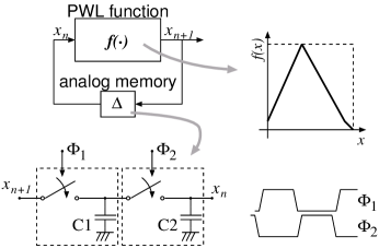
Interest in the hardware implementation of chaotic systems has recently been boosted by the expectations in fields such as communication systems [8], biologically-inspired computation [4], noise generation, EMI reduction [12], etc. Many applications depend on the existence of pseudo-random data streams of given statistical properties and can directly benefit from chaos-based generators. In fact, the collocation of chaos at the borderline between randomness and causality can be deployed for building extremely simple analog CMOS noise-like sources characterized by small areas and power requirements [5, 3]. These are commonly based on discrete time models like the one in Figure 1 [5, 6].
Note that for the implementation of the individual building blocks, the current mode approach is currently the best established one. Regrettably, the systems proposed so far exhibit a limited data rate which hinders their applicability. Even with unconventional design optimizations [1], it is difficult to rise data rates over a few .
Herein we propose the addressing of throughput issues by means of hardware resources replication and parallel operation. Particularly, we propose a technique for order-2 concurrency which allows two identical independent chaotic sources to share a large amount of their hardware. The approach is validated by: i. analytical results about major output statistical properties; ii. an application example to an FM-DCSK communication system [8] and iii. the simulation of a sample circuit designed over a conventional CMOS technology and capable of .
Analog register options
With reference to the model in Figure 1 and to operating frequencies, one of the most critical sections is the memory which is required for keeping stable while the map circuit evaluates . Analog operation is a pre-requisite for truly chaotic behaviour, yet this introduces errors in the in-loop signal path which must be kept extremely low as they have an immediate impact on the output statistics of the chaotic source [2]. As expectable, speed-accuracy trade-off do normally exist.
Since the analog memory synchronizes the circuit to an external clock and is never allowed to provide a transparent connection from input to output, its operation is actually as the analog counterpart of a digital register. Just as a digital register, it can be built up of more elementary latching elements, in this case sample-and-hold (SH) or track-and-hold (TH) units. Hence, three main degrees of freedom are allowed to the designer: choice of the register architecture, the choice in between TH or SH elements, and the choice of the particular circuit for the SHs or THs. Obviously, the three choices are interrelated.
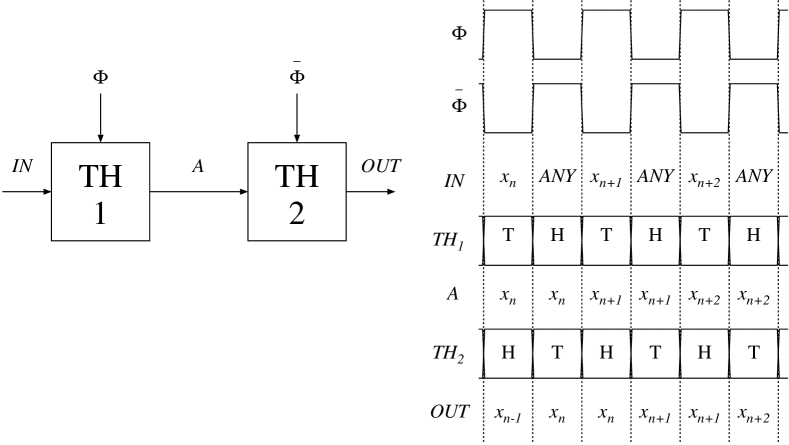
For what concerns the register architecture and the preference to SHs or THs, it can be noticed that correct operation can be obtained either by cascading TH elements (as shown in Figures 1 and 2),
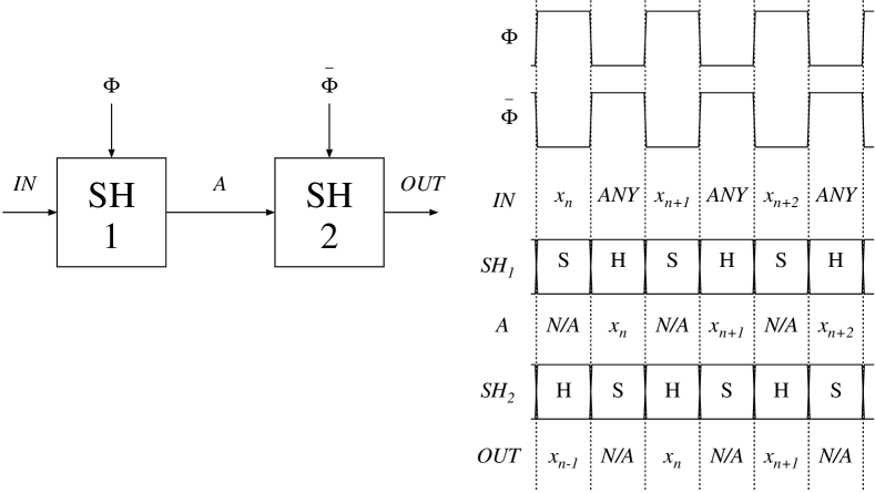
by cascading SH elements (Figure 3),
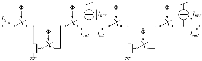
or by having two SH elements operating in anti-parallel (Figure 4).
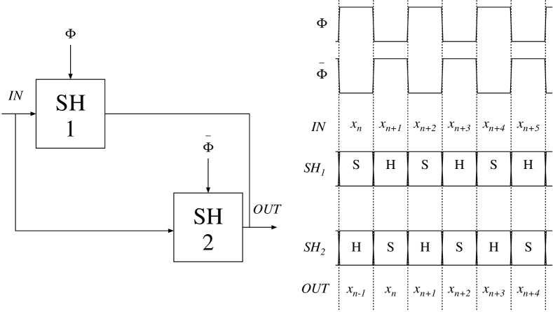
Note that in the current mode design approach, SH circuits (dynamic current mirrors) show many advantages (e.g. the absence of device matching issues) over THs and are generally preferred. The figures show also the timing diagrams where the differences are justified by the fact that TH circuits can provide a valid output during the sampling phase, while SHs can not. From the over-mentioned figures it is evident that the cascaded circuits can process a new sample at every clock period, while the anti-parallel one is capable of a new sample every half clock period and is inherently faster. Of course, in a practical circuit this is important only if it is the analog register itself to be the speed limiting factor, yet in chaotic circuits this is often the case.
Thus, was it not for other design issues, there would be no doubt for preferring the anti-parallel SH solution. Actually, this is where the third degree of freedom, i.e. the choice of a particular SH circuit comes into play.
As mentioned above, in-loop errors must be kept extremely low, so that optimized SH architectures must be selected. When discussing the accuracy of analog memory element a distinction among signal independent and signal dependent errors comes natural, so that, in current mode operation, one writes:
| (1) |
where the three addends on the righthandside represent the ideal behaviour, the signal dependent and the signal independent error respectively. Discrete time chaotic circuit are known to be more sensitive to signal dependent errors [2].
In current mode operation, the cascade of two SH (or TH) stages has the property of allowing the cancellation of signal independent errors, as long as the matching among the two stages is sufficiently good. For instance, one can easily arrange things in the spirit of the sample circuit of Figure 5, where:
| (2) |
Note is a suitably large current, and that the time-indexes , etc. have been omitted for simplicity. The output current is thus
| (3) |
where is the overall signal dependent error.
Hence there is an opportunity of selecting SH circuits specially optimized for reducing signal dependent errors, then relying on SH cascading for the reduction of signal independent ones. In this way the signal dependent errors to which chaotic circuits are most sensitive can be addressed at their best, within each SH unit, while less critic signal independent errors can be dealt with at the register level exploiting the SH matching properties. For instance, in [1] it is proposed the adoption of SI SHs [7] which have the property of dealing extremely well with signal dependent errors regardless of matching, while leaving a relatively large residual signal independent error.
Because of the signal independent error cancellation property, the cascaded SH analog register architecture is often preferable to the anti-parallel one. Unfortunately, this does normally mean sacrificing the operating speed of the anti-parallel topology. In the following, an interleaving technique is proposed which allows retaining the advantages of both worlds.
Interleaving
If two cascaded-SH analog registers are themselves connected in anti-parallel, then the topology and the timing diagrams shown in Figure 6 are obtained.
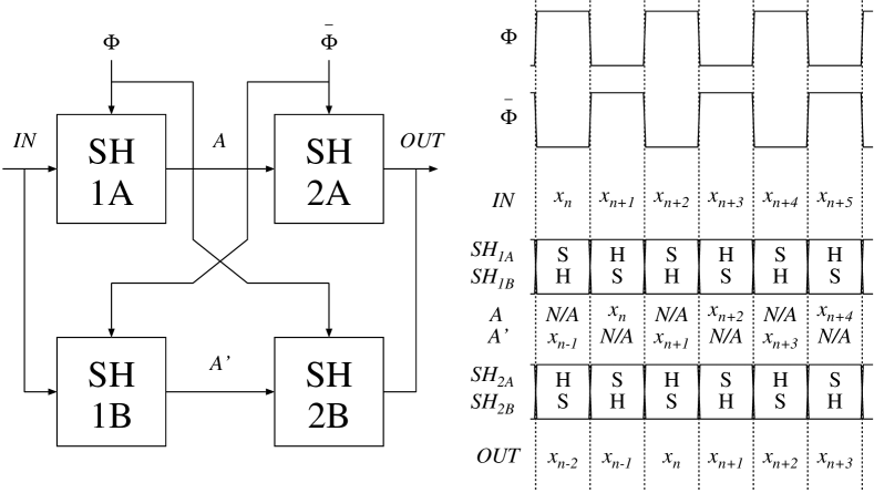
Note that this architecture provides cancellation of SH signal independent errors. Furthermore, it has the same throughput as the architecture in Figure 4, i.e. a new sample every half clock cycle. The only difference is the associated delay: in the topology of Figure 4 the output is delayed half a clock cycle with regard to input, while in the topology of Figure 6 the delay is a whole clock cycle.
This means that if the architecture shown in Figure 6 is substituted for the analog memory in the discrete time system given in Figure 1, still one cannot obtain a chaotic circuit providing a new chaotic sample every half clock cycle. However, two independent identical chaotic sources showing interleaved operation can be obtained, as it will be illustrated shortly.
Let us accept that these two systems exist, and name them ‘(A)’ and ‘(B)’. Suppose that the sample in Figure 6 corresponds to the initial condition of system ‘(A)’ and that corresponds to the initial condition of system ‘(B)’. If the clock period is and at the analog register outputs , then from to the map circuit operates on producing . At the same time, the analog register samples , hence . From to the analog register provides , causing the map circuit to operate on . Thus the map provides and the register samples . From to , the register outputs , i.e. , the map computes , which is in turn sampled as . From to , the register outputs , i.e. and the map computes which is sampled as and so on.
It is self-evident how two different chaotic trajectories emerging from the same map are kept separated in a time-division fashion. In general terms, the information stored on the interleaved analog register can be related to the state of the chaotic systems as:
| (4) |
In other words, the SHs marked ‘A’ in Figure 6 store and transfer the state of system ‘A’, while those marked ‘B’ store the state of system ‘B’.
The two systems are obviously independent, since there is no exchange of information among the two. What remains to be seen is if the sequences and are themselves independent in a cross-correlation sense. What if at startup the initial conditions and are identical? Being the dynamic chaotic, there is actually no worry about synchronization. In fact, sensitivity to initial conditions assures that the trajectories of system ‘(A)’ and ‘(B)’ cannot help rapidly diverging because of the unavoidable mismatch in the initial conditions and the effects of noise. Note that this would be true of any two independent chaotic sources based on the same map, yet this arrangement is particularly convenient, as it allows to realize two identical chaotic sources while sharing a large part of their hardware (the whole map circuit) and to obtain an output sample every half clock cycle.
At this point, it is interesting to consider the statistical properties of the interleaved sequence at the output of the analog register, and to verify whether they can be useful to some applications.
If we consider the sequence , its probability density function (PDF) is of course the same as that of (or ). Hence, interleaving does not influence the first order statistics. On the contrary, the autocorrelation is obviously affected. In fact we have:
| (5) |
where is the average (or DC component) of the sequences and , that we shall assume to be zero for simplicity. If we take the Fourier transform of the autocorrelation we obtain the power density spectrum, resulting in:
| (6) |
which can be rewritten as
| (7) |
where is the clock period. Hence, being a periodic function, the power density spectrum is not affected. Higher order moments, which are harder but not impossible to compute, are generally all affected, but they have a lower impact on typical applications.
Application example
In order to show an example in which an interleaved chaotic source is adopted instead of a traditional one, we shall consider an FM-DCSK communication system [10, 9]. In an FM-DCSK modulator, a discrete time uniform PDF random/chaotic source is used as the input to an FM modulator. In this way a spread-spectrum band-pass carrier is obtained to be fed to a further DCSK modulator, as shown in Figure 7. Ideally the spread spectrum carrier should be characterized by a bandwidth limited to an interval and by a uniform power density spectrum over that interval.
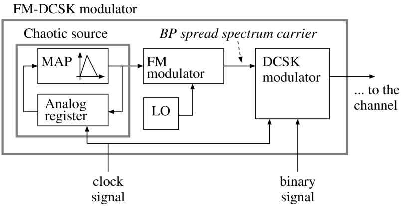
If one looks at a practical case of the so called fast FM-DCSK, where a random source is used to drive the FM modulator, a spectrum as the one in Figure 8 (top-left) is obtained for the signal out of the DCSK modulator. The non-uniform power distribution is clearly given by the FM modulation index which is used in practical fast FM-DCSK systems.
If a uniform PDF white-spectrum chaotic source is used instead of a random source, then the spectral characteristics of the DCSK carrier are somehow slightly deteriorated. Typically, the closer to one the mixing rate of the chaotic process [11], the more perceptible the influence on the spectrum. Easy to implement chaotic systems (such as tent-map based ones) show mixing rates which allow to perceive the spectral deterioration, but still allow a satisfying behaviour. Top-right plot in Figure 8 shows the spectral properties of the FM-DCSK signal when a chaotic tent-map base process is used to feed the FM modulator.


In practice, it is common to use chaotic models where particular strategies are adopted to enhance the implementation robustness. An example is offered by tailed tent map (TTM) systems [3], such as:
| (8) |
where is a control parameter in usually taken very close to zero. By adopting a TTM chaos generator () the FM-DCSK signal spectrum is modified as shown by the bottom left plot in Figure 8.
Finally, the bottom right plot shows the spectral properties of a DCSK signal generated using an interleaved TTM based chaotic source. In this case not only the applicability of the interleaving technique is verified: a slightly better behaviour is also obtained. This improvement is due to the effects of the interleaving technique on the higher order moments of the chaotic process. However note that the impact on the overall behaviour of a complete FM-DCSK system is almost negligible. However, the possibility of using an interleaved source is extremely interesting, since it allows to design chaotic sources capable of reaching the data rate requirements of FM-DCSK modulators. As a reference value, consider that typical systems designed so far require .
Sample circuit
In order to show the effectiveness of the proposed technique, a sample circuit has been designed and simulated. For this testing a well established CMOS technology has been adopted. The circuit has been designed to reach an output data rate sufficient for the FM-DCSK application illustrated above.
The schematic that we illustrate is based on [1], where SI dynamic mirrors [7] are used for enhanced speed and accuracy. The TTM is chosen as the system nonlinear function.
The map circuit is shown in Figure 9.
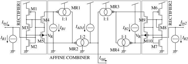
Note that it requires two identical input currents to perform concurrently the comparisons necessary to evaluate the relative position of the input and the breakpoints. For this evaluation active circuits are used, so that the main feature of the circuit is that the voltage at the inputs can be kept almost constant. In [1], a convenient way is suggested to make this voltage generally available by means of a dummy rectifier. This allows to use in other parts of the circuit, for instance to connect the wells of M5 and M10, cancelling the body effect and improving performance.
Reference currents and are set respectively to and and set the breakpoint positions (). Currents and () speed up signal processing by never allowing mirrors to operate on null currents. Finally, () fixes the output offset and sets the system invariant set to . Current mirrors are all high swing cascode and gate areas of transistors that could introduce matching errors are always non-minimal (typically ¿ ).
The analog delay is shown in Figure 10.
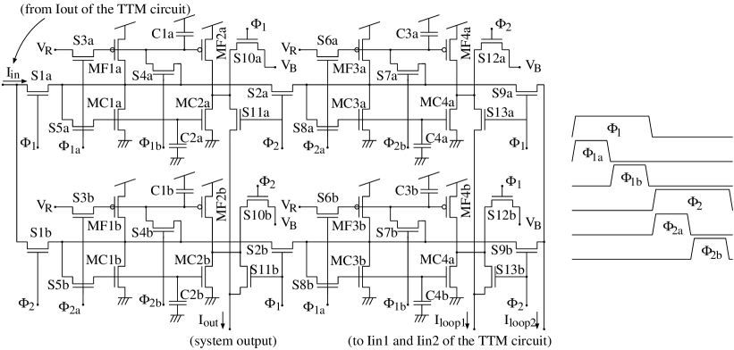
This already comprises two interleaved memory units, each of them built up of two SI dynamic current mirrors [7]. The clocking scheme is as for a typical SI system and the unit embeds mirroring to provide currents to both the map circuit inputs and the chaotic system output. For convenience in Figure 10 the two interleaved analog memories are distinguished by the postfixes “a” or “b” applied to all the relevant devices, while the many switches are named Sxxx.
Note that (as pointed out in [1]) for correct interfacing to the map circuit, the voltage mentioned above must be used as the reference voltage for the SI dynamic mirrors in order to exploit the low input impedance of the map unit (in the figure, is simply a buffered version of ). This circuit ideally propagates the state variables without introducing signal dependent errors, which is an important condition for the accurate operation of the chaotic system. Only the output variable is subject to a non-negligible sampling error, which is an offset and thus easy to deal with.
Figure 11

shows the evolution of the output variable when the system is simulated using SPICE with accurate analog device models (BSIM 3). The output data rate is .
The observation of longer sequences has shown that the unavoidable coupling among the two interleaved chaotic systems due to circuit parasitic does not produce perceivable effects such as synchronization. Direct estimation of statistical properties from spice data has proven hard, due to the inefficiency of SPICE time-step algorithms when dealing with SI circuits. In practice, it has not been possible to obtain long enough sequences for reliable statistics estimation. Nonetheless, a mix of Spice and behavioural simulations has allowed to obtain the plots in Figures 12 and 13. The first refers to the probability density function and the second to the power density spectrum of the state variable which is propagated through the analog register.


Conclusions
In this paper, the use of an interleaving technique applied to discrete time chaotic sources has been proposed. Its feasibility has been analytically shown and the usability of the so obtained chaotic sources for a sample application (FM-DCSK communication) has been verified by simulations at the model level.
To validate the possibility of exploiting the proposed technique at the hardware level, a CMOS circuit has been designed using a conventional technology. As far as simulations have been ran, the circuit has shown operation in accordance with the expected behaviour. Some data is still lacking about the estimation of the spectral properties of the hardware interleaved chaotic generator.
Currently work is in progress, both in order to obtain good estimation of the statistical properties of the system directly from circuit simulation and to evaluate the usability of interleaved chaotic sources to other application fields.
The authors
Sergio Callegari and Riccardo Rovatti are with the Department of
Electronics, Computer Science and Systems (DEIS) of the University of
Bologna, Viale Risorgimento 2, 40137 - Bologna (ITALY).
E-mail:
scallegari@deis.unibo.it
rrovatti@deis.unibo.it
Gianluca Setti is with the Department of Information Science (DI) of
the University of Ferrara, Via Saragat 1, 44100 - Ferrara (ITALY).
E-mail:
gsetti@ing.unife.it
References
- [1] S. Callegari, R. Rovatti, and G. Setti. A tailed tent map chaotic circuit exploiting S2I memory elements. In Proceedings of ECCTD’99, volume 1, Stresa, September 1999.
- [2] Sergio Callegari and Riccardo Rovatti. Sample and hold errors in the implementation of chaotic maps. In Proceedings of NOLTA’98, volume 1, pages 199–202, Crans Montana, September 1998.
- [3] Sergio Callegari, Gianluca Setti, and Peter J. Langlois. A CMOS Tailed Tent Map for the generation of uniformly distributed chaotic sequences. In Proceedings of IEEE ISCAS’97, volume 2, pages 781–784, Hong Kong, June 1997.
- [4] T. G. Clarkson, C. K. Ng, and J. Bean. Review of hardware pRAMs. Neural Networks World, (5):551–564, 1993.
- [5] M. Delgado-Restituto, F. Medeiro, and A. Rodríguez-Vázquez. Nonlinear, switched current CMOS IC for random signal generation. Electronics Letters, (25):2190–2191, 1993.
- [6] R. Devaney. An introduction to Chaotic Dynamical Systems. Addison Wesley, 2nd edition, 1989.
- [7] J. B. Hughes and K. W. Moulding. S2I: a two step approach to switched currents. In Proceedings of IEEE ISCAS’93, volume 2, pages 1235–1238, 1993.
- [8] M. P. Kennedy. Chaotic communications: State of the art. In Proceedings of ECCTD’99, volume 1, Stresa, September 1999.
- [9] G. Kolumban and B. Frigyik. Robust chaotic communication without synchronization. In Proceedings of ECCTD’99, pages 445–448, Stresa, August 1999.
- [10] G. Kolumban, G. Kis, Z. Jako, and M. P. Kennedy. FM-DSCK: a robust modulation scheme for chaotic communications. IEICE Transactions on Fundamentals, E81-A(9):1798–1802, 1998.
- [11] A. Lasota and M. C. Mackey. Chaos, Fractals and Noise. Stochastic Aspects of Dynamics. Springer-Verlag, 2nd edition, 1995.
- [12] R. Rovatti, G. Setti, and S. Graffi. Chaos based FM of clock signals for EMI reduction. In Proceedings of ECCTD’99, volume 1, Stresa, September 1999.