Behavior of grain boundaries in CuInSe2 and CuGaSe2 photovoltaic absorbers as revealed by first-principles hybrid functional calculations
Abstract
The inconclusive results of the previous first-principles studies on the grain boundaries (GBs) in CuInSe2 reveal the importance of employing a method that can correctly describe the electronic structure of this solar-cell material. We have employed hybrid functional calculations to study the (112) and (114) GBs in CuInSe2 and CuGaSe2. The electronic structure changes introduced by the formation of GBs are threefold: creation of gap states, shift in band edges, and alteration of bandgap sizes. Gap states commonly behave as recombination centers, but the band alignment and the change in the bandgap size induced by GBs mitigate the destructive effect of these states in CuInSe2. That means, GBs are not detrimental for the carrier transport in devices based on CuInSe2. Conversely, these GBs are destructive for the carrier transport in CuGaSe2. The different behaviors of the GBs in CISe and CGSe might be considered by experimentalists to optimize the device fabrication to achieve high-performance solar cells.
pacs:
61.72.Mm, 71.15.Mb, 61.72.BbI Introduction
Thin-film solar cells based on Cu(In,Ga)Se2 (CIGSe) are fabricated and deployed worldwide on an industrial scale due to their outstanding price/performance ratio Chirila et al. (2013); Jackson et al. (2015). In contrast to silicon-based solar cells Seager et al. (1979), the efficiency of CIGSe cells with polycrystalline light absorber exceeds the efficiency of their monocrystalline counterpart Rau et al. (2009). This is remarkable, because typically the performance of optoelectronic devices is considered to be worse for polycrystalline semiconductors due to the presence of grain boundaries (GBs). GBs are expected to create deep gap levels that act as recombination centers and are commonly regarded detrimental for the solar-cell performance. Despite the extensive studies carried out in the past decades to investigate the effects of GBs on the efficiency of CIGSe-based solar cells, their role remains a topic of intense debate.
In the literature, different atomic structures for symmetric GBs in CuInSe2 and CuGaSe2 have been reported. Abou-Ras et al. Abou-Ras et al. (2012) identified and studied experimentally two types of (112) GBs in CuInSe2: Se-Se-terminated {112} plane GBs and cation-Se-terminated {112} plane GBs. While the former showed Cu depletion and In enrichment, Cu depletion without In enrichment was detected for the latter. Yan et al. Yan et al. (2006), on the other hand, reported no change in the atomic composition near the cation-Se-terminated {112} plane GBs. This discrepancy could be due to different methods employed to study the atomic composition Hetzer et al. (2005); Lei et al. (2007). Another type of GB, namely (114), has been studied in CuInSe2 and CuGaSe2 Yan et al. (2007); Li et al. (2011); Yin et al. (2013); Feng et al. (2014). Although this type of GB is not experimentally identified in CuInSe2 and CuGaSe2, its structure is adopted from GBs in CdTe. A common feature of the GBs is that high percentage of these GBs in CuInSe2 and CuGaSe2 are charge neutral Baier et al. (2011); Siebentritt et al. (2006); Jiang et al. (2012).
Due to the complex nature of thin-film devices, it would be highly desirable to achieve new insights from theoretical calculations. Such results can serve as common ground between experimentalists and theoreticians leading to a better understanding of the properties of devices. Taking advantage of the calculated results makes experimentalists able to improve the cells in the laboratory scale. Consequently these knowledge can be transferred to the industrial scale.
The outcomes of the previous first-principles studies on GBs, however, are not conclusive Persson and Zunger (2003); Yan et al. (2006); Li et al. (2011); Yan et al. (2007); Yin et al. (2013); Feng et al. (2014). In their pioneering work, Persson and Zunger Persson and Zunger (2003) employed LDA and LDA+U method to study the cation-terminated (112) surface of CuInSe2 to explain the anomalous characteristics of the symmetric GBs. They proposed that the valence band maximum (VBM) of the surface is lower than the bulk VBM therefore the GBs act as a hole barrier. The Cu vacancy reconstruction at the surface, which lowers the surface VBM with respect to the bulk VBM, is in contrast to the results of Yan et al. Yan et al. (2006). Other authors employed different flavors of (local) LDA and (semi-local) GGA to study the (114) GBs in CuInSe2 and CuGaSe2. While some studies Yan et al. (2007); Li et al. (2011) suggested that these GBs do not create any gap state, the other studies predicted the formation of deep gap states in the bandgap of the systems with GBs Yin et al. (2013); Feng et al. (2014).
The results achieved by (semi-) local methods remain doubtful, even if they are in agreement with experimental findings. This is because of the employed methods in the aforementioned studies that do not describe the semiconducting nature of CuInSe2 and CuGaSe2 adequately Hinuma et al. (2013); Pohl and Albe (2013). Namely, for the defect-free CuInSe2 and CuGaSe2 bulk, the bandgaps predicted by PBE and PBE+U are severely underestimated 111In our calculations, the CuInSe2 bulk bandgap calculated by PBE+U method is 0.14 eV.. This failure is partly due to the shortcomings of (semi-) local methods and partly due to underestimation of the anion displacement () of CuInSe2 Vidal et al. (2010). The size of the bandgap is of particular importance when the defect states, which might appear in the bandgap, are studied. In light of the shortcomings of the underlying methods, the inconsistencies between previous works are not surprising. In this work we report on the first-principles hybrid functional study of two types of GBs, namely (112) and (114), in CuInSe2 and CuGaSe2.
II Methodology
Hybrid functionals are known as a rather accurate method to study the electronic structure of semiconductors. In this approach a portion of the exact exchange calculated by Hartree-Fock method is incorporated into the exchange-correlation functional calculated by density functional theory (DFT). In the present work, we used HSE06 functional Heyd et al. (2003) with the fraction of the exact exchange set to 30 % Pohl et al. (2011); Hinuma et al. (2012, 2013). Using this setup, the value of the anion displacement is calculated with an error smaller than 0.3 % and the computed bandgaps are 1.0 eV and 1.6 eV for CuInSe2 and CuGaSe2, respectively, in agreement with experimental values Alonso et al. (2001).
All calculations have been performed within the framework of DFT as implemented in Vienna Ab-initio Simulation Package (VASP) Kresse and Furthmüller (1996). We used the projector augmented wave (PAW) Blöchl (1994); Kresse and Joubert (1999) method together with a plane-wave cutoff energy of 300 eV and a mesh of () k-points. For density of states (DOS) calculations a denser k-mesh has been used. The supercells consist of 128 and 180 atoms for the (112) and (114) GBs, respectively. To construct the supercells, the optimized lattice constants and atomic positions of the bulk have been used. The distance between periodic supercells separated by vacuum is about 30 Å.
Slab calculations, which are generally employed to represent a material with GBs, might suffer from the charge transfer through the slabs due to dangling bonds at the surfaces of the slabs. To quench the dipole moment of the slabs and prevent charge transfer, the surface dangling bonds were passivated with hydrogen-like pseudoatoms with partial charges. The valency of these hydrogen-like pseudoatoms are chosen in such a way that they provide the amount of missing electrons for the surface atoms, so they fulfill the octet rule. The position of atoms in the outer four atomic layers were fixed to their bulk position to mimic the underlying bulk material. Other atoms were fully relaxed until the forces on each atom were below 0.01 eV/Å. Using the same methodology, a defect-free supercell with {112}-plane termination was constructed and considered as the reference.
To evaluate the relative shift of the VBM and conduction band minimum (CBM) with respect to the bulk, the macroscopic average of the electrostatic potentials are calculated Dandrea and Duke (1993); Alkauskas et al. (2011); D'Amico et al. (2012); Komsa et al. (2012). The VBM shift can be expressed as
| (1) |
where is the energy difference from the VBM to the reference level of system ‘1’ and is the energy difference from the VBM to the reference level of system ‘2’, see FIG. 1. The energy difference and are calculated in the region far form the GBs and are very close the values calculate for the perfect periodic bulk. By knowing the size of the bandgap, the CBM shift calculation is straightforward.

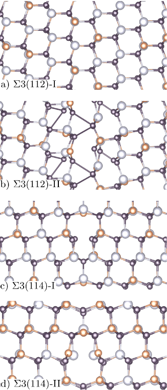
The crystal structure of Cu(In,Ga)Se2 and CdTe has the same fundamental characteristics and the GBs in CuInSe2 and CuGaSe2 can be modeled based on the observed GB structures in CdTe. In the present work, (112) and (114) correspond to lamellar and double-positioning twins in CdTe Yan et al. (2001, 2003). In the (112) GBs, either a cation-containing plane is next to a Se-containing plane ((112)-I) or Se-containing planes are facing each other ((112)-II). In the (114) GBs, either Se atoms have dangling bonds ((114)-I) or cations have dangling bonds ((114)-II). The atomic structure of the (112) and (114) GBs are very different: while the (114) GBs contain dangling, wrong, and extra bonds the atomic structure of (112)-I is very similar to the bulk and the (112)-II GB contains Se dangling and Se-Se wrong bonds.
III Results and discussion
The atomic structures of GBs in CuInSe2 after geometry optimization are presented in FIG. 2. While (112)-I shows little changes in its structure, (112)-II undergoes dramatic structural relaxation. Compared to the bulk, Se atoms at the (112)-II GB are not surrounded by four cations. After optimization, the minimum distance between Se atoms increases from 3.11 Å to 3.52 Å. In contrast to CuInSe2, Se atoms at the (112)-II GB of CuGaSe2 (not shown here) are not located at the outermost layer of the GB: on one side of the GB Se atoms migrate into the bulk and instead of Se-Se wrong bonds at the GBs, Se-cation bonds are formed. In a qualitative agreement with the previous studies Yan et al. (2007); Yin et al. (2013), in the (114) GBs the atoms with dangling bonds show larger relaxation compared to the other atoms.
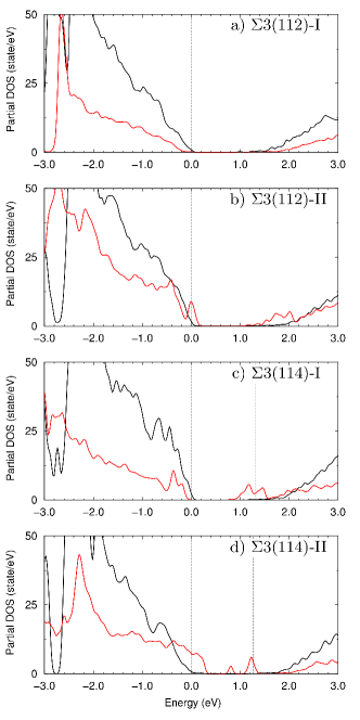
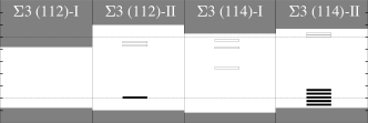
It has been discussed that dangling and wrong bonds in CdTe can create defect levels Zhang et al. (2008). Since the (114) and (112)-II GBs contain these defects, one expects to see defect levels in the bandgap of the systems with these GBs as well. To study the effects of the GBs on the electronic structure, we calculated atom-projected partial DOS for the systems with GBs. The projected partial DOS for the (112) and (114) GBs in CuInSe2 are shown in FIG. 3. All GBs (except (112)-I that creates no gap state) create unoccupied gap states close to the CBM which are in resonance with the conduction band states in agreement with the simulations Mönig et al. (2010). From the total energy of the charged ( and ) GBs we have computed the thermodynamic charge transition levels. In CuInSe2 and CuGaSe2, the positively-charged GBs are not stable but the defect states can trap electrons to make the GBs negatively charged.
Our data show that the existence of GBs shifts the VBM and CBM with respect to the bulk VBM and CBM. This can lead to ‘electron-free’/‘hole-free’ zone near the GBs where the concentration of electrons/holes is less than in the grain interior (GI). It has been discussed that the creation of such a barrier at the GBs for one type of the carrier (electron or hole) impedes electron-hole recombination at the GBs Persson and Zunger (2003, 2005); Gloeckler et al. (2005). FIG. 4 schematically presents the computed band offsets between the GB and GI for CuInSe2 and CuGaSe2.
The other effect of the GBs on the electronic structure is to change the size of the bandgap. In the case of CuInSe2, the systems containing (112)-I, (112)-II, (114)-I, and (114)-II have the bandgap size of 1.0 eV, 1.4 eV, 1.3 eV, and 1.3 eV, respectively. For the corresponding GBs in CuGaSe2 the bandgaps are 1.6 eV, 1.6 eV, 1.8 eV, and 1.8 eV, respectively. In the following paragraphs, we give a detailed discussion of our findings for different types of GBs.
in CuInSe2 and CuGaSe2, the (112)-I GBs do not create gap states but shift the VBM and CBM with respect to the bulk (FIG. 4). This band alignment draws electrons to the GB region but reflects holes away. The electron-hole recombination remains low because of insufficient holes at the GB. This GB forms easily in Cu(In,Ga)Se2 due to its highly symmetric structure Baier (2012) and is harmless for the carrier transport.
the (112)-II GB in CuInSe2 creates three gap states: one occupied state which is 0.1 eV above the VBM and two unoccupied states which are 0.3 eV and 0.4 eV below the CBM. The level is not in the bandgap, therefore holes are not trapped in the defect states. The level is in the bandgap, positioned 0.2 eV below the CBM. This defect level can be occupied by electrons only if CuInSe2 is n-type. Our results are in agreement with the experimentally-observed charge-neutral (112) GBs in p-type CuInSe2 Baier et al. (2011). In the system containing this type of GB, the VBM and CBM are 0.2 eV lower and higher than the bulk VBM and CBM, respectively (see FIG. 4, top panel). This band alignment expels electrons and holes from the GB region. These electronic properties of the (112)-II GBs in CuInSe2 explain why this type of GB is harmless for the carrier transport in p-type CuInSe2.
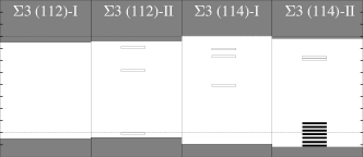
In the case of CuGaSe2, the level is not in the bandgap but is 1.5 eV below the CBM. Hence, electrons from the conduction band can be trapped in this level. Considering the band alignment (FIG. 4, bottom panel), both the VBM and CBM of this system are 0.2 eV lower than the VBM and CBM of the bulk. That is, while this GB creates an electrostatic barrier for holes, concentration of electrons close to this GB is higher than in the GI. The valence band offset, however, is not large enough to suppress the holes concentration at the GB Gloeckler et al. (2005) therefore the carrier lifetime is reduced if this type of the GB is formed in CuGaSe2.
as it is shown in FIG. 3 (c), the dangling and wrong bonds of the (114)-I GB in CuInSe2 cause unoccupied gap states to form. The deepest unoccupied state is 0.5 eV below the CBM. The and charge transition levels are 0.7 eV and 0.5 eV below the CBM and VBM, respectively. Thus, the positively-charged gap states are not stable but the defect levels can trap electrons and become negatively charged. The band offset of this system, however, screens this GB from bulk carriers and results in low probability of recombination.
Formation of the (114)-I GBs in CuGaSe2 creates three unoccupied gap states. The level is 1.2 eV below the CBM, therefore the defect levels can trap electrons even for a p-type CuGaSe2. Holes, on the other hand, cannot be trapped in the defect levels. The conduction band offset (FIG. 4, bottom panel) makes the region close to this GB electron rich. The motion of holes into the GB region, on the other hand, is impeded due to the valence band offset. The size of the valence band offset, however, is not large enough to mitigate the effect of the presence of this GB in the system Gloeckler et al. (2005).
the cation dangling bonds create both occupied and unoccupied states in the bandgap of CuInSe2 and CuGaSe2. For CuInSe2 (see FIG. 3 (d)), the occupied gap states are close to the VBM and the deepest state is 0.2 eV above the VBM. The deepest unoccupied gap state is 0.1 eV below the CBM. The level is not in the gap and is 0.5 eV below the CBM. This means, positively-charged gap states are not stable but if the chemical potential of the electrons is high, i. e. n-type CuInSe2, then electrons can be trapped in the defect levels. Still, the electron- and hole-free zone near this GB make the probability of recombination low.
The VBM and CBM of this GB in CuGaSe2 are 0.3 eV and 0.1 eV below the bulk VBM and CBM, respectively. The transition level is not in the gap and is 0.9 eV below the CBM. This GB remains neutral for p-type CuGaSe2 but for high chemical potential of the electrons, the gap states can become negatively charged. The conduction band offset for this GB (FIG. 4, bottom panel) also leads to a high concentration of electrons close to the GB, meaning that the chance of electrons to be trapped in the gap state is high. Although the valence band offset repels holes from the GB, it cannot effectively screen the GB from holes and this GB is prone to recombination Gloeckler et al. (2005).
We note that in our study the electronic-structure changes are merely due to the existence of the GBs. To look into the influence of changing the chemical potential of the constituent atoms, we have studied the effect of the formation of a charge-neutral defect pair () on the electronic structure of (112)-II in CuInSe2. In agreement with previous results Persson and Zunger (2003), the VBM is lower than the bulk VBM. In this system, the occupied gap state is removed from the bandgap but the unoccupied gap states are still present.
IV Summary
In summary, our results are the following: (i) to study GBs in Cu(In,Ga)Se2, employing a method that can correctly describe the electronic structure of this material, hybrid functional for example, is essential. (ii) The formation of GBs can alter the electronic structure of their systems in three different ways: a) GB creates gap states, b) GB shifts the VBM and CBM with respect to the bulk, and c) GB changes the bandgap size. (iii) Although gap states can be detrimental for the carrier transport, the band offsets and the change in the bandgap sizes mitigate this destructive effect in CuInSe2. (iv) The behavior of the GBs in CuGaSe2 is different from CuInSe2. The conduction band offset draws electrons to the GB region and the valence band offset is not large enough to suppress the concentration of holes. This band offset makes the presence of the symmetric GBs in CuGaSe2 destructive, except for the (112)-I GB.
The electrically benign behavior of the GBs in CuInSe2 suggests that the GBs in this material do not need passivation. The detrimental behavior GBs in CuGaSe2, on the other hand, shows the necessity of the GBs passivation. Our findings could be of interest to the research groups seeking to optimize the device fabrication and to improve the efficiency of the solar cells based on Cu(In,Ga)Se2.
V Acknowledgment
We acknowledge the financial support from the Bundesministerium für Wirtschaft und Energie (BMWi) for the comCIGS II project (0325448C).
References
- Chirila et al. (2013) A. Chirila, P. Reinhard, F. Pianezzi, P. Bloesch, A. Uhl, C. Fella, L. Kranz, D. Keller, C. Gretener, H. Hagendorfer, D. Jaeger, R. Erni, S. Nishiwaki, S. Buecheler, and A. Tiwari, Potassium-induced surface modification of Cu(In, Ga)Se2 thin films for high-efficiency solar cells, Nature Mater. 12, 1107 (2013).
- Jackson et al. (2015) P. Jackson, D. Hariskos, R. Wuerz, O. Kiowski, A. Bauer, T. M. Friedlmeier, and M. Powalla, Properties of Cu(In, Ga)Se2 solar cells with new record efficiencies up to 21.7%, physica status solidi (RRL) – Rapid Research Letters 9, 28 (2015).
- Seager et al. (1979) C. H. Seager, G. E. Pike, and D. S. Ginley, Direct measurement of electron emission from defect states at silicon grain boundaries, Phys. Rev. Lett. 43, 532 (1979).
- Rau et al. (2009) U. Rau, K. Taretto, and S. Siebentritt, Grain boundaries in Cu(In, Ga)(Se, S)2 thin-film solar cells, Applied Physics A 96, 221 (2009).
- Abou-Ras et al. (2012) D. Abou-Ras, B. Schaffer, M. Schaffer, S. S. Schmidt, R. Caballero, and T. Unold, Direct insight into grain boundary reconstruction in polycrystalline Cu(In, Ga)Se2 with atomic resolution, Phys. Rev. Lett. 108, 075502 (2012).
- Yan et al. (2006) Y. Yan, R. Noufi, and M. M. Al-Jassim, Grain-boundary physics in polycrystalline CuInSe2 revisited: Experiment and theory, Phys. Rev. Lett. 96, 205501 (2006).
- Hetzer et al. (2005) M. J. Hetzer, Y. M. Strzhemechny, M. Gao, M. A. Contreras, A. Zunger, and L. J. Brillson, Direct observation of copper depletion and potential changes at copper indium gallium diselenide grain boundaries, Applied Physics Letters 86, 162105 (2005).
- Lei et al. (2007) C. Lei, C. M. Li, A. Rockett, and I. M. Robertson, Grain boundary compositions in Cu(InGa)Se2, Journal of Applied Physics 101, 024909 (2007).
- Yan et al. (2007) Y. Yan, C.-S. Jiang, R. Noufi, S.-H. Wei, H. R. Moutinho, and M. M. Al-Jassim, Electrically benign behavior of grain boundaries in polycrystalline CuInSe2 films, Phys. Rev. Lett. 99, 235504 (2007).
- Li et al. (2011) J. Li, D. B. Mitzi, and V. B. Vivek, Structure and electronic properties of grain boundaries in earth-abundant photovoltaic absorber Cu2ZnSnSe4, ACS Nano 5, 8613 (2011).
- Yin et al. (2013) W.-J. Yin, Y. Wu, R. Noufi, M. Al-Jassim, and Y. Yan, Defect segregation at grain boundary and its impact on photovoltaic performance of CuInSe2, Applied Physics Letters 102, 193905 (2013).
- Feng et al. (2014) C. Feng, M. Luo, B. Li, D. Li, J. Nie, and H. Dong, Benefits of oxygen in CuInSe2 and CuGaSe2 containing Se-rich grain boundaries, Physics Letters A 378, 1956 (2014).
- Baier et al. (2011) R. Baier, D. Abou-Ras, T. Rissom, M. C. Lux-Steiner, and S. Sadewasser, Symmetry-dependence of electronic grain boundary properties in polycrystalline CuInSe2 thin films, Applied Physics Letters 99, 172102 (2011).
- Siebentritt et al. (2006) S. Siebentritt, S. Sadewasser, M. Wimmer, C. Leendertz, T. Eisenbarth, and M. C. Lux-Steiner, Evidence for a neutral grain-boundary barrier in chalcopyrites, Phys. Rev. Lett. 97, 146601 (2006).
- Jiang et al. (2012) C.-S. Jiang, M. A. Contreras, I. Repins, H. R. Moutinho, Y. Yan, M. J. Romero, L. M. Mansfield, R. Noufi, and M. M. Al-Jassim, How grain boundaries in Cu(In, Ga)Se2 thin films are charged: Revisit, Applied Physics Letters 101, 033903 (2012).
- Persson and Zunger (2003) C. Persson and A. Zunger, Anomalous grain boundary physics in polycrystalline CuInSe2: The existence of a hole barrier, Phys. Rev. Lett. 91, 266401 (2003).
- Hinuma et al. (2013) Y. Hinuma, F. Oba, Y. Kumagai, and I. Tanaka, Band offsets of CuInSe2/CdS and CuInSe2/ZnS (110) interfaces: A hybrid density functional theory study, Phys. Rev. B 88, 035305 (2013).
- Pohl and Albe (2013) J. Pohl and K. Albe, Intrinsic point defects in CuInSe2 and CuGaSe2 as seen via screened-exchange hybrid density functional theory, Phys. Rev. B 87, 245203 (2013).
- Note (1) In our calculations, the CuInSe2 bulk bandgap calculated by PBE+U method is 0.14 eV.
- Vidal et al. (2010) J. Vidal, S. Botti, P. Olsson, J.-F. M. C. Guillemoles, and L. Reining, Strong interplay between structure and electronic properties in CuIn(S, Se)2: A first-principles study, Phys. Rev. Lett. 104, 056401 (2010).
- Heyd et al. (2003) J. Heyd, G. E. Scuseria, and M. Ernzerhof, Hybrid functionals based on a screened coulomb potential, The Journal of Chemical Physics 118, 8207 (2003).
- Pohl et al. (2011) J. Pohl, A. Klein, and K. Albe, Role of copper interstitials in CuInSe2: First-principles calculations, Phys. Rev. B 84, 121201 (2011).
- Hinuma et al. (2012) Y. Hinuma, F. Oba, Y. Kumagai, and I. Tanaka, Ionization potentials of (112) and (11) facet surfaces of CuInSe2 and CuGaSe2, Phys. Rev. B 86, 245433 (2012).
- Alonso et al. (2001) M. I. Alonso, K. Wakita, J. Pascual, M. Garriga, and N. Yamamoto, Optical functions and electronic structure of CuInSe2, CuGaSe2, CuInS2, and CuGaS, Phys. Rev. B 63, 075203 (2001).
- Kresse and Furthmüller (1996) G. Kresse and J. Furthmüller, Efficient iterative schemes for ab initio total-energy calculations using a plane-wave basis set, Phys. Rev. B 54, 11169 (1996).
- Blöchl (1994) P. E. Blöchl, Projector augmented-wave method, Phys. Rev. B 50, 17953 (1994).
- Kresse and Joubert (1999) G. Kresse and D. Joubert, From ultrasoft pseudopotentials to the projector augmented-wave method, Phys. Rev. B 59, 1758 (1999).
- Dandrea and Duke (1993) R. G. Dandrea and C. B. Duke, Calculation of the schottky barrier height at the Al/GaAs(001) heterojunction: Effect of interfacial atomic relaxations, Journal of Vacuum Science & Technology A 11, 848 (1993).
- Alkauskas et al. (2011) A. Alkauskas, P. Broqvist, and A. Pasquarello, Defect levels through hybrid density functionals: Insights and applications, Physica Status Solidi (b) 248, 775 (2011).
- D'Amico et al. (2012) N. R. D'Amico, G. Cantele, and D. Ninno, First principles calculations of the band offset at SrTiO3-TiO2 interfaces, Applied Physics Letters 101, 141606 (2012).
- Komsa et al. (2012) H.-P. Komsa, T. T. Rantala, and A. Pasquarello, Finite-size supercell correction schemes for charged defect calculations, Phys. Rev. B 86, 045112 (2012).
- Yan et al. (2001) Y. Yan, M. M. Al-Jassim, and T. Demuth, Energetics and effects of planar defects in CdTe, Journal of Applied Physics 90, 3952 (2001).
- Yan et al. (2003) Y. Yan, M. M. Al-Jassim, and K. M. Jones, Structure and effects of double-positioning twin boundaries in CdTe, Journal of Applied Physics 94, 2976 (2003).
- Zhang et al. (2008) L. Zhang, J. L. F. Da Silva, J. Li, Y. Yan, T. A. Gessert, and S.-H. Wei, Effect of copassivation of Cl and Cu on CdTe grain boundaries, Phys. Rev. Lett. 101, 155501 (2008).
- Mönig et al. (2010) H. Mönig, Y. Smith, R. Caballero, C. A. Kaufmann, I. Lauermann, M. C. Lux-Steiner, and S. Sadewasser, Direct evidence for a reduced density of deep level defects at grain boundaries of Cu(In, Ga)Se2 thin films, Phys. Rev. Lett. 105, 116802 (2010).
- Persson and Zunger (2005) C. Persson and A. Zunger, Compositionally induced valence-band offset at the grain boundary of polycrystalline chalcopyrites creates a hole barrier, Applied Physics Letters 87, 211904 (2005).
- Gloeckler et al. (2005) M. Gloeckler, J. R. Sites, and W. K. Metzger, Grain-boundary recombination in Cu(In, Ga)Se2 solar cells, Journal of Applied Physics 98, 113704 (2005).
- Baier (2012) R. Baier, Electronic grain boundary properties in polycrystalline Cu(In, Ga)Se2 semiconductors for thin film solar cells, Ph.D. thesis, Helmholtz-Zentrum Berlin für Materialien und Energie (2012).