Graphene on transition-metal dichalcogenides: a platform for proximity spin-orbit physics and optospintronics
Abstract
Hybrids of graphene and two dimensional transition metal dichalcogenides (TMDC) have the potential to bring graphene spintronics to the next level. As we show here by performing first-principles calculations of graphene on monolayer MoS2, there are several advantages of such hybrids over pristine graphene. First, Dirac electrons in graphene exhibit a giant global proximity spin-orbit coupling, without compromising the semimetallic character of the whole system at zero field. Remarkably, these spin-orbit effects can be very accurately described by a simple effective Hamiltonian. Second, the Fermi level can be tuned by a transverse electric field to cross the MoS2 conduction band, creating a system of coupled massive and massles electron gases. Both charge and spin transport in such systems should be unique. Finally, we propose to use graphene/TMDC structures as a platform for optospintronics, in particular for optical spin injection into graphene and for studying spin transfer between TMDC and graphene.
Graphene spintronics Han et al. (2014) has relied exclusively on electrical spin injection Tombros et al. (2007); Pi et al. (2010); Yang et al. (2011). Combining graphene with semiconducting two-dimensional TDMC Mak et al. (2010) can open new venues for spintronics applications Žutić et al. (2004); Fabian et al. (2007). Indeed, TMDC are becoming increasingly popular in optoelectronics as sensitive photodetectors Lopez-Sanchez et al. (2013) or, forming lateral heterostructures Huang et al. (2014); Lee et al. (2014), as two-dimensional solar cells Pospischil et al. (2014). Important, TMDC have a sizeable spin-orbit coupling and lack space inversion symmetry. As a result, their band structure Kormányos et al. (2015) allows for a valley resolved optical spin excitation by circularly polarized light Xiao et al. (2012); Mak et al. (2012); Zeng et al. (2012). TMDC can thus facilitate optical spin injection into graphene, in hybrid structures.
Efficient growth of MoS2 on graphene has already been demonstrated Lin et al. (2014a, b); Azizi et al. (2015). It was reported that graphene on MoS2 is ultraflat, having large mean free paths Lu et al. (2014); angle-resolved photoemission found an intact Dirac point but a strong hybridization elsewhere in the system Coy Diaz et al. (2015). Technological potentials for these hybrid structures are already being discussed Kumar et al. (2015), mainly as a basis for nonvolatile memory Bertolazzi et al. (2013), sensitive photodetection Zhang et al. (2014), and gate-tunable persistent photoconductivity Roy et al. (2013). Recently, the spin Hall effect in graphene on few-layer WS2 was observed at room temperature Avsar et al. (2014).
In this paper we establish by first-principles calculations fundamental electronic properties and the spin-orbit fine structure of the graphene Dirac bands for graphene on monolayer MoS2, and introduce an effective spin-orbit Hamiltonian which explains the proximity induced spin splittings of the Dirac states. We show that the induced spin-orbit coupling is giant, being 20 times more than in pristine graphene. We also discuss the field effect on the band offsets of the two materials. Finally, we present possible experimental schemes to perform optical spin injection into graphene and study spin tunneling from TMDC through graphene.
First-principles results.
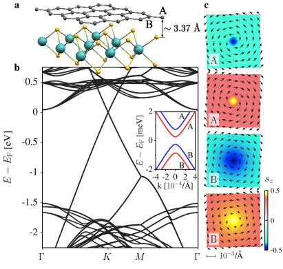
To establish the electronic and spin properties of graphene on MoS2 we used first-principles methods based on density-functional theory Hohenberg and Kohn (1964), see Methods. To reduce structural strain we constructed a large supercell of 59 atoms, comprising a supercell of MoS2 and a supercell of graphene, with the residual lattice mismatch of 1.4%. The relaxed interlayer distance between graphene and MoS2 is 3.37 Å, see Fig. 1a). In this supercell the point of MoS2 is mapped to the point in the reduced Brillouin zone. The calculated electronic band structure is shown in Fig. 1b). The Dirac cones of graphene are nicely preserved, with the projected Dirac point (which is also the Fermi level) being slightly below the conduction band edge of MoS2. The closeness of the Dirac point to the conduction band of MoS2 enhances screening, which can substantially increase the mean free path in the graphene layer, as recently shown experimentally Lu et al. (2014).
The band offsets between graphene and MoS2 can be controlled by an external electric field applied transverse to the layers. This is demonstrated by our first-principles calculations in Fig. 2a), where we present , the difference between the conduction band minima of MoS2 and graphene. At negative fields (pointing towards MoS2) the offset increases, leaving both layers neutral. However, positive fields shift the Dirac point above the conduction band minimum of MoS2 and populate graphene with holes and MoS2 with electrons. The Fermi level crosses both the valence band of graphene and the conduction band of MoS2, see Fig. 2b) and c). This field effect can establish a unique system in which massless Dirac electrons are coupled with a conventional 2d electron gas Scharf and Matos-Abiague (2012).
We now zoom in on the Dirac point at to see how the electronic spectrum of graphene deforms in the presence of MoS2. This fine structure is shown in the inset to Fig. 1b). There are two important effects: First, an orbital band gap opens, due to the breaking of the graphene pseudospin symmetry. On average, atoms and in the graphene supercell see a different environment coming from the MoS2 layer. This orbital gap is there even in the absence of spin-orbit coupling. It arises from the effective staggered potential induced by the pseudospin symmetry breaking. Second, spin-orbit coupling combined with the broken space inversion symmetry lifts the spin degeneracy of the Dirac valence and conduction bands and leads to the appearance of four distinct bands. This splitting is on the meV scale, which is giant when compared to the 24 eV spin-orbit splitting in pristine graphene Gmitra et al. (2009). The inset also shows the orbital character of the bands at : while the valence states are formed at the sublattice, the conduction states live on . The same orbital ordering is at .
Another important characteric of the Dirac states is their spin texture. This is plotted in Fig. 1c) for the four bands from the inset of Fig. 1b). Directly at the spins are pointing out of the graphene plane, alternating up and down. Increasing the momentum away from , the spins acquire a winding in-plane component, either clockwise or counterclockwise, suggestive of the strong Rashba effect. At the spins are reversed.

Effective Hamiltonian.
Can we understand these proximity-induced changes in graphene’s band structure from an effective model? The answer is not obvious since not only sublattices and differ, but even the sites that belong to the same sublattice see different local environments in the supercell. Surprisingly, an effective symmetry-based Hamiltonian with graphene orbitals in the presence of pseudospin inversion symmetry breaking gives a remarkably good description. The model builds on the orbital Hamiltonian for pristine graphene which, close to () points, is
| (1) |
Here is the Fermi velocity of graphene, and are the Cartesian components of the electron wave vector measured from , parameter for , and and are the pseudospin Pauli matrices acting on the two-dimensional vector space formed by the two triangular sublattices of graphene. Hamiltonian describes gapless Dirac states with the conical dispersion near the Dirac points; for the conduction (valence) band.
The staggered potential describing the effective orbital energy difference on and sublattices of graphene on MoS2 enters via the Hamiltonian,
| (2) |
where is the pseudospin Pauli matrix and is the unit spin matrix; is the proximity induced gap of the Dirac spectrum. Another consequence of the pseudospin inversion asymmetry is the sublattice-resolved intrinsic spin-orbit coupling. Indeed, the intrinsic coupling acts solely on a given sublattice: it is a next-nearest neighbor hopping Konschuh et al. (2010). We describe it in our model with parameters and for sublattices and , respectively. The corresponding proximity induced spin-orbit coupling Hamiltonian close to ,
| (3) |
is a generalization of the McClure-Yafet Hamiltonian for graphene McClure and Yafet (1962); Han et al. (2014). We denote by the spin Pauli matrix, while by the unit matrix acting on the pseudospin (sublattice) space. If , the main effect of the intrinsic spin-orbit coupling is to enhance the anticrossing of the pristine graphene Dirac cones Gmitra et al. (2009), leaving the spin degeneracy intact. However, if , as in our case, the spin degeneracy gets lifted by this intrinsic term already, reflecting the loss of space inversion symmetry.
Placing graphene on MoS2 also breaks the lateral mirror symmetry, giving rise to the Rashba type spin-orbit coupling Konschuh et al. (2010),
| (4) |
where is the Rashba parameter and , are the spin Pauli matrices. In the hopping language, the Rashba coupling is the nearest-neighbor spin-flip hopping, contributing further to the spin splitting of the bands, and defining the spin quantization axis for each Bloch state, away from the time reversal points and .
Hamiltonian fully describes graphene’s bands at . Its eigenenergies are
| (5) |
where for spin up (down) branches. The expectation values of the spin along for the corresponding states are given by
| (6) |
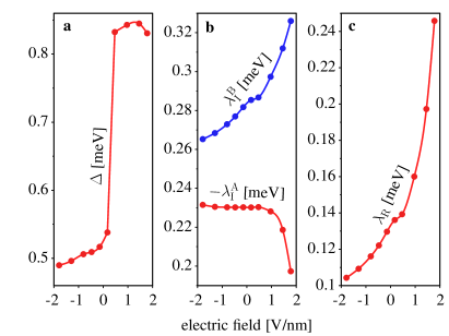
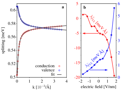
Using the formulas for the eigenenergies, Eq.(Effective Hamiltonian.), and for the spin expectation values, Eq.(6), we can algebraically extract the orbital band gap and the three spin-orbit parameters , , and by comparing to our first-principles data for the fine structure at , see the inset to Fig. 1b). The extracted parameters are shown in Fig. 3 as a function of the applied transverse electric field. The orbital proximity gap is about 0.5 meV in zero field. In fields greater than 0.5 V/nm, the gap exhibits a steep increase, which is related to the transfer of the electronic charge from graphene to MoS2, see Fig. 2. The proximity spin-orbit parameters in Fig. 3b) and c) are about 0.2 meV, which is 20 times more than in pristine graphene Gmitra et al. (2009). Similar giant values of spin-orbit coupling in graphene are induced by hydrogen adatoms Neto and Guinea (2009); Gmitra et al. (2013); Balakrishnan et al. (2013), and even more by fluorine Irmer et al. (2015), though the mechanisms are different. Unlike in the adatom cases in which the induced spin-orbit coupling is only local, in our case the giant coupling is global. While the intrinsic parameters and change rather moderately with applying the electric field, the Rashba parameter , see Fig. 3c), more than doubles in increasing the field from -2 to 2 V/nm.
What is the origin of the induced giant spin-orbit coupling in graphene on MoS2? We trace the enhancement to the hybridization of the carbon orbitals with the -orbitals of Mo. We find only 0.3% of -orbitals at the point by analyzing the calculated density of states. But when we turn the spin-orbit coupling on Mo atoms in the supercell off, the orbital gap in zero field remains almost unchanged ( meV), while the spin-orbit parameters drop to their pristine graphene values , and , which are, curiosly, also determined by orbitals, but from carbon atoms Gmitra et al. (2009).
Away from , the spin splittings depend on the momentum. In order to describe our first-principles data, we add the PIA (pseudospin inversion asymmetry) spin-orbit coupling term Gmitra et al. (2013) which, like the intrinsic coupling, represents the next nearest neighbor hopping, but with a spin flip. The full model Hamiltonian describes the data perfectly, see Supplementary information.
Although our effective model should capture the basic physics of graphene on TMDC, the extracted parameters are for the specific supercell of graphene on MoS2. Certainly, taking an even larger cell that could further reduce strain, or twisting the two layers as could happen in experiments, would lead to a different set of parameters, although the orders of magnitudes would likely stay. In a macroscopic experimental structure we expect Moire patterns which would transform our Hamiltonian into a Hamiltonian density, with an orbital gap and spin-orbit fields, perhaps even averaging some of the parameters (such as and the difference between and ) to zero. Our extraxted parameters can then be viewed as effective standard deviations of the spatial variations, suitable as input for charge and spin transport model calculations for such samples. We also expect that graphene on TMDC could produce superlattice features as in graphene on hBN Gorbachev et al. (2014).
| a |
 |
| b |
 |
Optospintronics.
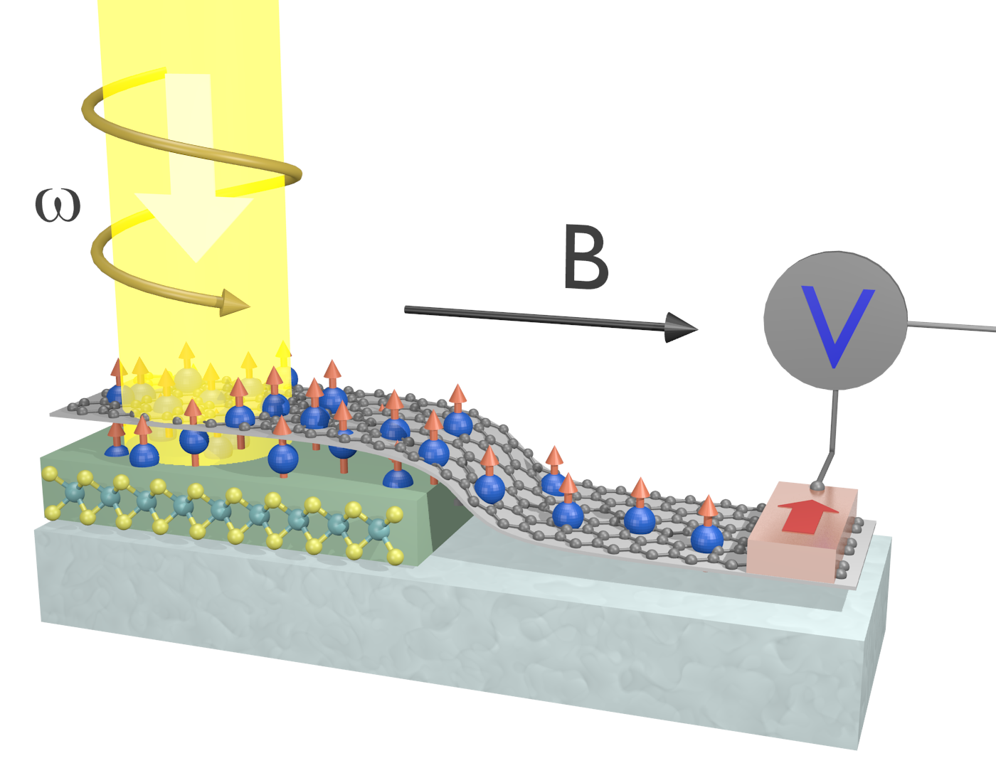
We propose graphene-TMDC hybrids, such as the one studied above based on MoS2, as an ideal platform for optospintronics. In Fig. 4a) we give an optical spin injection scheme into graphene. A circularly polarized light, tuned to the band gap of TMDC, excites electron spins by optical orientation Meier and (Eds.); Žutić et al. (2004). In effect, the light produces spin-polarized excitons which dissociate into spin-polarized electrons and holes. As in the recent optical experiment Roy et al. (2013), we expect that electrons will be transfered to graphene, leaving holes behind in TMDC, although in which way electrons and holes split may depend on the TMDC material as well as on gating. The spin-polarized electrons (or holes) diffuse in graphene. One can detect this spin accumulation either optically, by observing a circular polarization of the photoluminescence Meier and (Eds.) elsewhere in graphene on TMDC, or electrically. The latter is illustrated in Fig. 4a): a ferromagnetic electrode on top of graphene detects the presence of the spin accumulation in graphene Žutić et al. (2004); Fabian et al. (2007). Spin precession in graphene can be observed as the Hanle signal (which is not possible to see in the spin-valley coupled TMDC Sallen et al. (2012)), by applying an external magnetic field transverse to the injected spin, providing Larmor precession Fabian et al. (2007).
Spin transport per se in graphene-TMDC bilayers should be fascinating. The presence of the giant, effectivelly uniform spin-orbit fields should give large spin Hall signals, even greater than in hydrogenated graphene Balakrishnan et al. (2013). Most important, as our calculations show, the spin, like charge, properties of these structures are expected to be highly field tunable. The fascinating prospect of realizing the massive-massless electron gas coupling of the two electron gases, if the Fermi level is positioned in both band structures, calls for new theories of spin transport and spin relaxation in such hybrid systems.
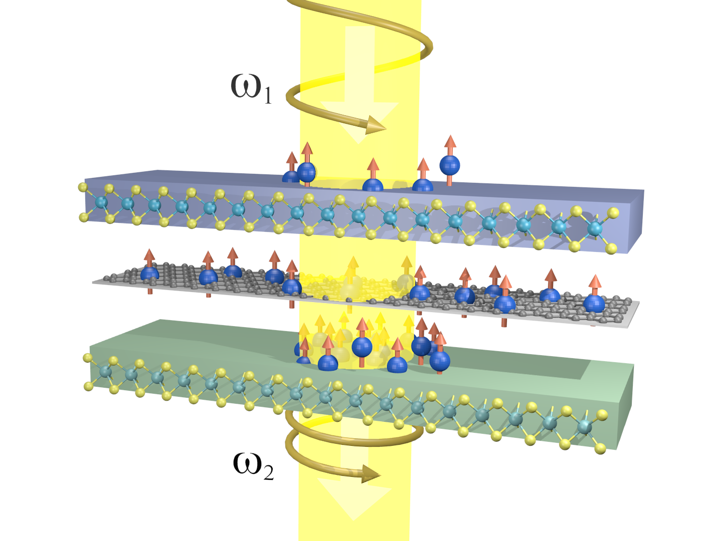
To demonstrate spin tunneling from a TMDC through graphene one could use a sandwich structure, as pictured in Fig. 4b). The two semiconductors have different band gaps, allowing to discern the photoluminesence signals from the top and bottom layers. If the spin pumping light is tuned to the band gap of the top layer, the spin-polarized carriers would be excited there and tunnel through graphene to the bottom layer, in which they would recombine and emit circularly-polarized light with the frequency characteristics of the bottom material. One can envision influencing the signal with a transverse magnetic field, allowing for a Hanle effect Another possibility is to measure the accumulated spin in the bottom layer using the magneto-optical Kerr effect, as in recent experiments on monolayer MoS2 Plechinger et al. (2014).
Conclusion.
We have established by first-principles calculations a strong effect of MoS2 on the spin properties of graphene, predicting a giant and field-tunable proximity spin-orbit coupling for Dirac electrons. We have introduced an effective spin-orbit Hamiltonian to describe the electronic states around the Fermi level, fitting perfectly the first-principles data. We have also showed that gating can tune the band offsets of the two layers, allowing to realize the unique system of coupled massless and massive electron gases. Finally, we have proposed to use graphene on TMDC as a platform for optospintronics with graphene-based two-dimensional materials structures.
Acknowledgements.
We thank T. Korn, C. Schüller, C. Stampfer, B. Beschoten, T. Müller, and B. Özyilmaz for useful descussions and hints regarding possible experimental realizations of optospintronics with graphene-TMDC structures. This work was supported by DFG SFB 689, GRK 1570, and by the EU Seventh Framework Programme under Grant Agreement No. 604391 Graphene Flagship.Supplementary information
.1 Methods
Structural relaxation and electronic structure calculations were performed with Quantum ESPRESSO Giannozzi and et al. (2009), using norm conserving pseudopotentials with kinetic energy cutoff of 60 Ry for wavefunctions. For the exchange-correlation potential we used generalized gradient approximation Perdew et al. (1996). The supercell containing a supercell of MoS2 and supercell of graphene was embeded in a slab geometry with vacuum of about 13 Å, with a dipole correction Bengtsson (1999), which is crucial to get accurate band offsets between the Dirac point and the conduction band minimum of MoS2. The resulting structure has a lattice mismatch of 2.8% which we split equally between graphene and MoS2 by compressing graphene and stretching MoS2 by 1.4%. The supercell has 59 atoms. The reduced Brillouin zone was sampled with k points. Atomic positions were relaxed using the quasi-newton algorithm based on the trust radius procedure including the van der Waals interaction which was treated within a semiempirical approach Grimme (2006); Barone et al. (2009). The calculated work function on the graphene side is 4.12 eV, while on MoS2 it is 4.41 eV.
.2 Spin eigenstates
The normalized eigenstates at the point of the Hamiltonian discussed in the manuscript in the basis read
| (7) |
where and . The eigenvectors are ordered with increasing energy (using the extracted parameters): . Analyzing the above eigenvectors we see that the valence bands are localized on sublattice , while the conduction bands on sublattice . The component of the spin alternates from band to band. This behavior matches the first-principles results, see inset to Fig. 1b) in the manuscript. The top valence and bottom conduction states are pure pseudospin and spin states. On the other hand, spin-orbit coupling mixes spin and pseudospin of the outermost states. The eigenstates at have the same form, but opposite spins.
.3 PIA coupling: spin splitting away from
To describe the calculated spin splittings away from , we employ the PIA (short for pseudospin inversion asymmetry) spin-orbit term, introduced to study the effects of spin-orbit coupling in graphene due to hydrogen adatoms Gmitra et al. (2013):
| (8) |
Here and are the spin-orbit parameters representing the average, , and differential, , PIA coupling between the and sublattices. Like intrinsic spin-orbit coupling, PIA can be also represented by next-nearest-neighbor (same sublattice) hopping, but with a spin flip. The PIA terms turn the spin quantization axes of the electron states towards the graphene plane and add to the Rashba term for momenta away from the point.
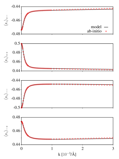
To obtain and we add to the Hamiltonian , which is used directly at in the manuscript, and fit to the first-principles data, keeping all other parameters as determined directly at . In Fig. 5a we plot the calculated spin splittings of the valence and conduction bands. The full model, with PIA, fits the first-principles data perfectly. The fits are meVÅ, and meVÅ. In Fig. 5b we plot the two PIA parameters as functions of the applied transverse electric field. Their tunability is enormous, much more than that of the Rashba hopping shown in the manuscript. As a final check we calculate, using the extracted parameters, the components of the spin expectation values in the vicinity of the point for the low energy states. The model is fully consistent with the first-principles data, as seen in the comparison plotted in Fig. 6.
References
- Han et al. (2014) W. Han, R. K. Kawakami, M. Gmitra, J. Fabian, M. Gmitra, R. K. Kawakami, and W. Han, Nature Nanotechnology 9, 794 (2014).
- Tombros et al. (2007) N. Tombros, C. Józsa, M. Popinciuc, H. T. Jonkman, and B. J. van Wees, Nature 448, 571 (2007).
- Pi et al. (2010) K. Pi, W. Han, K. M. McCreary, A. G. Swartz, Y. Li, and R. K. Kawakami, Phys. Rev. Lett. 104, 187201 (2010).
- Yang et al. (2011) T.-Y. Yang, J. Balakrishnan, F. Volmer, A. Avsar, M. Jaiswal, J. Samm, S. R. Ali, A. Pachoud, M. Zeng, M. Popinciuc, et al., Phys. Rev. Lett. 107, 047206 (2011).
- Mak et al. (2010) K. F. Mak, C. Lee, J. Hone, J. Shan, and T. F. Heinz, Phys. Rev. Lett. 105, 136805 (2010).
- Žutić et al. (2004) I. Žutić, J. Fabian, and S. Das Sarma, Rev. Mod. Phys. 76, 323 (2004).
- Fabian et al. (2007) J. Fabian, A. Matos-Abiague, C. Ertler, P. Stano, and I. Žutić, Acta Phys. Slovaca 57, 565 (2007).
- Lopez-Sanchez et al. (2013) O. Lopez-Sanchez, D. Lembke, M. Kayci, A. Radenovic, and A. Kis, Nature Nanotechnology 8, 497 (2013).
- Huang et al. (2014) C. Huang, S. Wu, A. M. Sanchez, J. J. P. Peters, R. Beanland, J. S. Ross, P. Rivera, W. Yao, D. H. Cobden, and X. Xu, Nature Materials 13, 1096 (2014).
- Lee et al. (2014) C.-H. Lee, G.-H. Lee, A. M. van der Zande, W. Chen, Y. Li, M. Han, X. Cui, G. Arefe, C. Nuckolls, T. F. Heinz, et al., Nature Nanotechnology 9, 676 (2014).
- Pospischil et al. (2014) A. Pospischil, M. M. Furchi, and T. Mueller, Nature Nanotechnology 9, 257 (2014).
- Kormányos et al. (2015) A. Kormányos, G. Burkard, M. Gmitra, J. Fabian, V. Zólyomi, N. D. Drummond, and V. Fal’ko, 2D Materials 2, 022001 (2015).
- Xiao et al. (2012) D. Xiao, G.-B. Liu, W. Feng, X. Xu, and W. Yao, Phys. Rev. Lett. 108, 196802 (2012).
- Mak et al. (2012) K. F. Mak, K. He, J. Shan, and T. F. Heinz, Nature Nanotechnology 7, 494 (2012).
- Zeng et al. (2012) H. Zeng, J. Dai, W. Yao, D. Xiao, and X. Cui, Nature Nanotechnology 7, 490 (2012).
- Lin et al. (2014a) Y.-C. Lin, N. Lu, N. Perea-Lopez, J. Li, Z. Lin, X. Peng, C. H. Lee, C. Sun, L. Calderin, P. N. Browning, et al., ACS Nano 8, 3715 (2014a).
- Lin et al. (2014b) M.-Y. Lin, C.-E. Chang, C.-H. Wang, C.-F. Su, C. Chen, S.-C. Lee, and S.-Y. Lin, Appl. Phys. Lett. 105, 073501 (2014b).
- Azizi et al. (2015) A. Azizi, S. Eichfeld, G. Geschwind, K. Zhang, B. Jiang, D. Mukherjee, L. Hossain, A. F. Piasecki, B. Kabius, J. A. Robinson, et al., ACS Nano 9, 4882 (2015).
- Lu et al. (2014) C.-P. Lu, G. Li, K. Watanabe, T. Taniguchi, and E. Andrei, Phys. Rev. Lett. 113, 156804 (2014).
- Coy Diaz et al. (2015) H. Coy Diaz, J. Avila, C. Chen, R. Addou, M. C. Asensio, and M. Batzill, Nano Letters 15, 1135 (2015).
- Kumar et al. (2015) N. A. Kumar, M. A. Dar, R. Gul, and J. Baek, Materials Today 18, 286 (2015).
- Bertolazzi et al. (2013) S. Bertolazzi, D. Krasnozhon, and A. Kis, ACS Nano 7, 3246 (2013).
- Zhang et al. (2014) W. Zhang, C.-P. Chuu, J.-K. Huang, C.-H. Chen, M.-L. Tsai, Y.-H. Chang, C.-T. Liang, Y.-Z. Chen, Y.-L. Chueh, J.-H. He, et al., Sci. Rep. 4 (2014).
- Roy et al. (2013) K. Roy, M. Padmanabhan, S. Goswami, T. P. Sai, G. Ramalingam, S. Raghavan, and A. Ghosh, Nature Nanotechnology 8, 826 (2013).
- Avsar et al. (2014) A. Avsar, J. Y. Tan, T. Taychatanapat, J. Balakrishnan, G. K. W. Koon, Y. Yeo, J. Lahiri, A. Carvalho, A. S. Rodin, E. C. T. O’Farrell, et al., Nature Communications 5 (2014).
- Hohenberg and Kohn (1964) J. Hohenberg and W. Kohn, Phys. Rev. 136, B864 (1964).
- Scharf and Matos-Abiague (2012) B. Scharf and A. Matos-Abiague, Phys. Rev. B 86, 115425 (2012).
- Gmitra et al. (2009) M. Gmitra, S. Konschuh, C. Ertler, C. Ambrosch-Draxl, and J. Fabian, Phys. Rev. B 80, 235431 (2009).
- Konschuh et al. (2010) S. Konschuh, M. Gmitra, and J. Fabian, Phys. Rev. B 82, 245412 (2010).
- McClure and Yafet (1962) J. W. McClure and Y. Yafet, in Proceedings of the 5th conference on carbon (Pergamon Press, 1962), vol. 1, pp. 22–28.
- Neto and Guinea (2009) A. H. C. Neto and F. Guinea, Phys. Rev. Lett. 103, 026804 (2009).
- Gmitra et al. (2013) M. Gmitra, D. Kochan, and J. Fabian, Phys. Rev. Lett. 110, 246602 (2013).
- Balakrishnan et al. (2013) J. Balakrishnan, G. Kok, W. Koon, M. Jaiswal, and A. H. C. Neto, Nature Physics 9, 1 (2013).
- Irmer et al. (2015) S. Irmer, T. Frank, S. Putz, M. Gmitra, D. Kochan, and J. Fabian, Phys. Rev. B 91, 115141 (2015).
- Gorbachev et al. (2014) R. V. Gorbachev, J. C. W. Song, G. L. Yu, A. V. Kretinin, F. Withers, Y. Cao, A. Mishchenko, I. V. Grigorieva, K. S. Novoselov, L. S. Levitov, et al., 2D Materials 346, 448 (2014).
- Meier and (Eds.) F. Meier and B. P. Z. (Eds.), Optical Orientation (North-Holand, New York, 1984).
- Sallen et al. (2012) G. Sallen, L. Bouet, X. Marie, G. Wang, C. R. Zhu, W. P. Han, Y. Lu, P. H. Tan, T. Amand, B. L. Liu, et al., Phys. Rev. B 86, 081301 (2012).
- Plechinger et al. (2014) G. Plechinger, P. Nagler, Schüller, and T. Korn, arXiv:1404.7674 (2014).
- Giannozzi and et al. (2009) P. Giannozzi and et al., J.Phys.: Condens. Matter 21, 395502 (2009).
- Perdew et al. (1996) J. P. Perdew, K. Burke, and M. Ernzerhof, Phys. Rev. Lett. 77, 3865 (1996).
- Bengtsson (1999) L. Bengtsson, Phys. Rev. B 59, 12301 (1999).
- Grimme (2006) S. Grimme, J. Comput. Chem. 27, 1787 (2006).
- Barone et al. (2009) V. Barone, M. Casarin, D. Forrer, M. Pavone, M. Sambi, and Vittadini, J. Comput. Chem. 30, 934 (2009).