A Tailed Tent Map Chaotic Circuit Exploiting
S2I Memory Elements
Abstract
In the implementation of discrete time chaotic systems, designers have mostly focused on the choice and synthesis of suitable nonlinear blocks, while correct and fast operation cannot neglect analog memory elements. Herein, a realization exploiting the Tailed Tent Map coupled with S2I sample and hold stages is proposed. Interfacing problems between the memory and the processing sub-circuits are tackled and the possibility to obtain a fivefold speed improvement with respect to previously reported results is demonstrated by means of SPICE and other computer aided simulations.
1 Introduction
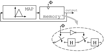
Several applications of chaotic hardware (like in secure communication schemes [1], noise generation, stochastic neural models [2], EMI reduction, etc.) can exploit even the simplest kind of chaotic systems, namely a one-dimensional map (Figure 1).
Although for obtaining chaotic behavior this arrangement requires a fully analog signal path, this does not prevent practical and compact CMOS realizations [3, 4, 5]. Indeed, interest in these systems has recently grown, mainly focusing on how to obtain useful statistical properties, on the design strategies, and on robustness issues [5]. In other words, the attention has been mainly devoted to the choice of suitable nonlinear maps and on their synthesis.
However, for truly effective operation, all the elements in the signal path (thus including the analog memory in the feedback loop) must be optimized having the requirements of a chaotic system in mind.
Recently, investigation in this direction has been proposed for a representative set of systems defined by piecewise-affine (PWA) maps and characterized by a uniform invariant probability density function (PDF) of the generated samples [6]. Two results of such investigation are that even maps which are traditionally considered robust with respect to implementation inaccuracies suffer from S/H errors and that, among all these errors, signal dependent ones seem to be the most critical.
Herein, we propose a system based on the most robust map among those considered in [6] — the Tailed Tent Map (TTM) (Figure 2)

[5] — coupled with one of the analog memory schemes which best address the signal dependent error issue, i.e. the S2I technology [7]. Not surprisingly, this allows to significantly relax the cycle time limitations and to improve the performance achievable with respect to previously presented results.
The system is designed with a standard n-well CMOS technology and allows an operating frequencies of at least — which stands out with regard to around in [5]. This is obtained at a very good level of esteemed accuracy and with internal currents as low as , for low-power operation.
2 Building blocks and interfacing
The abstract elements illustrated in Figure 1 are herein better investigated to illustrate the adoption of S2I and how consequent interfacing issues are tackled.
2.1 The Nonlinear map
The most common choice for designing PWA maps is the current mode approach. Figure 3 shows a framework in which current splitters are used to introduce breakpoints by operating as unidirectional devices. Splitters are arranged to operate in parallel to reduce propagation times.

The affine-combiner is implemented by means of mirrors and summing nodes. A splitter is required for every breakpoint, so that the TTM requires two of them (and two input currents).
The splitters/combiner pair is a potential bottleneck for high frequency operation since mirror transistors cannot be taken minimal size, as this would deteriorate their matching properties and the mirrors accuracy [8]. As a consequence, the extra-capacitance that has to be driven dictates very careful design. The proposed TTM circuit (Figure 4)
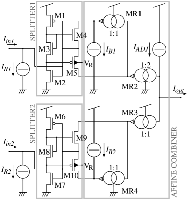
follows the current trend of adopting active splitters [3]. Exploiting an amplifier (M1-M2-M3 or M6-M7-M8), rather than simply adopting diodes or current mirrors [4] reduces the splitter input impedance, speeding up the system response which is commonly dominated by the product between input impedance and input capacitance. With regard to established designs (see e.g. [3]), three modifications are proposed:
-
i.
the adoption of transistors M3 and M8, bringing the input impedance further down by assuring that the voltage swing at the input capacitance is never larger than
(1) where is the threshold voltage of M4 (or M9), is its driving voltage, is the threshold voltage of M5 (or M10), is its driving voltage, is the threshold voltage of transistor M3 (or M8), is the diode driving voltage and is the gain of the inverting amplifier M1-M2-M3 (or M6-M7-M8);
-
ii.
the adoption of a dummy splitter driven by no current (Figure 5)

Figure 5: The dummy splitter used to generate . in order to generate a reference voltage to be applied to the well of the PMOS transistors M5 and M10. This avoids body effect, reduces in (1), and loads no extra capacitance on the input node as a well-source connection would do. If a twin well technology is available, it is convenient to tie also the bulks of M4 and M9 to ;
-
iii.
the adoption of bias currents, and , pumped into mirrors MR1 and MR4 to make sure that in no condition there are mirrors copying a null current. In fact, the step response time of a current mirror is mostly dependent on the step final current and grows very rapidly as this approaches zero.
As it will be seen in §2.3, the search for low input impedance is not just a matter of speed, but also of interfacing to S2I stages, so that the extra hardware required for the dummy splitter is effectively justified. Note also that the mirrors require cascode structures in order to minimize inaccuracies due to channel length modulation and finite output impedance. High-swing cascodes are suggested, as they have a limited hardware cost and they allow the stacking of the splitters and the mirrors at a power supply of . For suitable matching, gate areas of mirroring transistors must be no less than [8]. Finally, consider that reference currents and and the offset cancelling current can be selected among a range of values, with the result of changing the map invariant set. This degree of freedom will also be exploited in §2.3.
2.2 The S2I analog memory element
The memory element required for map iteration must transfer instantaneously the value at its input to the output when triggered by a clocking event, and at no time instant is allowed to become transparent. To achieve this, it is realized in a master-slave fashion cascading two sample-and-hold (S/H) circuits driven by opposite clock phases (balloon in Figure 1).

Its working principle is based on a two step sampling of the input current. First of all, MC samples the input current plus a certain reference current generated by MF, whose gate is connected to a reference voltage (phase ). After this first coarse sampling, the current on MC is where is an error mainly due to clock feed-through on switch S5. In the second step, MF samples the difference between the input current and the current stored on MC, i.e. (phase ). Phase is the hold phase. Also at the end of the fine sampling an error is committed, so that the final current stored on MF is . Hence, the output current of the S2I S/H is .
With this, even though an S2I S/H stage is not immune from sampling errors, the error is introduced while sampling a current always very close to so to be an (almost) signal independent error.
Moreover, a whole memory element is made of two S/H stages. In the case of S2I stages, two identical units can be directly cascaded, thanks to the presence of the reference current which makes an S2I S/H capable of dealing with both positive and negative input currents. This arrangement has the property of cancelling signal independent errors [9], so that the operation of a S2I 2 stage memory element is (theoretically) error free.
Note that, for cascading, the down-hill unit requires clocking signals complementary to those used in the up-hill one: in Figure 6, signals , and are meant to drive the second S/H. Clock phases are rigorously non-overlapping.
2.3 Interfacing
This section deals with the problem of interfacing a TTM circuit (§2.1) to an S2I memory element.
First of all, electrical interfacing will be considered. S2I circuits do not pose particular requirements to units driving them, but do pose constraints on the circuits being driven by them, since they are fundamentally designed to be cascaded to other S2I units. This is evident if one looks at the absence of cascode stages replacing over MC and MF, which may therefore be affected by channel length modulation. Errors are prevented by the fact that when an S2I unit is cascaded to another identical one, the fine sampling phase of the second unit guarantees the voltage at the drains of MC and MF to be approximately , i.e. the same voltage as at the end of the first unit sampling.
To prevent channel modulation error when driving a non-S2Istage without having to provide cascode structures for MC and MF, we need to adjust the input voltage of the circuit being driven by the down-hill S2I stage to be constantly as similar as possible to the used as a reference in the S2I circuits. To do so, a very low input impedance is needed.
Connecting to conventional mirrors is thus generally not feasible due to their non-negligible input impedance. What we propose is instead to connect the S2I memory element directly to the TTM circuit. In fact, this block has been designed for an extremely low input impedance (§2.1) and for an input voltage almost fixed at . The dummy splitter already introduced in §2.1 is here of great help as it can be exploited to generate .
The second point is functional interfacing. The TTM circuit requires two input currents. Furthermore, an additional current is necessary to read the output of the overall chaotic system. To cope with this, we propose to build current mirrors inside the S2I memory element. The final, complete circuit is shown in Figure 7.
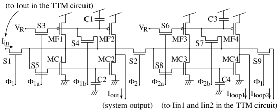
Such a circuit can be connected to the TTM circuit exploiting input and outputs and . is for reading the overall chaotic system output: it offers a time shifted (half clock cycle), complemented version of the system state variable. In the whole circuit this is the only signal subject to a non-compensated sampling error (which happens to be a constant offset not particularly troublesome for most applications). Note that mirroring inside the S2I subsystem introduces matching errors (which would anyway be introduced elsewhere in the signal path). To keep them low, all the MCx and the MFx transistors must be sized to have an area greater than . The consequence is a noticeable sampling error due to charge feed-through on the drain-to-gate capacitances of MCx and the MFx. Nonetheless proper device dimensioning can keep such error tolerable as confirmed by the the results in §3.
As a further consideration, note that sampling error may also be reduced by exploiting the ability of S2I S/H to cope with either positive or negative inputs and adopting a signal range centered on zero. In fact, this allows to use the smallest possible reference currents, to which errors are tied.
To do so, the values of , and can be chosen so that the system invariant set is centered around zero. The circuit has been simulated with , , and , so that the “state variable” currents are in the range.
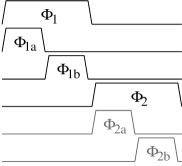
Finally, we shall briefly consider timings. Being the S2I dynamic mirror a sample-and-hold rather than a track-and-hold unit, it cannot deliver output while sampling. Hence, only half of clock cycle is left to the map circuit to elaborate its output (see Figure 8). While this poses constraints on the response time of the map circuit, it might (at least theoretically) allow interleaving of two analog memory elements on the same TTM circuit.

3 System simulation and conclusions
System simulations were run using SPECTRE, referring to charge-conservative BSIM3 device models. Figure 9

shows a collection of output samples as produced by the overall system. The operating frequency of is limited by the worst-case step response time of the TTM circuit (about — Figure 10) which corresponds to a step in the input current taking a splitter right over or below threshold.

To obtain a reliable estimation of the asymptotic statistical distribution of the system states in a reasonable amount of time, we have simulated the behavior of an open-loop system based on the TTM circuit together with the S2I subsystem, driven by a stepping signal spanning the whole range of operation of the TTM circuit (.TRAN analysis). Successively, the collected information has been used to build and interpolating behavioural model in C code. Finally, this efficient model has been iterated to produce the large number of samples required for PDF estimation. The result is reported in Figure 11 to show a good agreement with the theoretical expectations.

References
- [1] M. Hasler, “Syncronization principles and applications,” in Proceedings of the IEEE ISCAS (Tutorials), (London), pp. 314–327, May 1994.
- [2] T. G. Clarkson, C. K. Ng, and J. Bean, “Review of hardware pRAMs,” in Proceedings of WNNW’93 workshop, (York), pp. 18–23, Apr. 1993.
- [3] M. Delgado-Restituto, F. Medeiro, and A. Rodríguez-Vázquez, “Nonlinear, switched current CMOS IC for random signal generation,” Electronic Letters, no. 25, pp. 2190–2191, 1993.
- [4] P. J. Langlois, G. Bergmann, and J. Bean, “A current mode tent map with electrically controllable skew for chaos applications,” in Proceedings of NDES, (Dublin), 1995.
- [5] S. Callegari, G. Setti, and P. J. Langlois, “A CMOS Tailed Tent Map for the generation of uniformly distributed chaotic sequences,” in ISCAS97 proceedings, vol. 2, (Hong Kong), p. 781, June 1997.
- [6] S. Callegari and R. Rovatti, “Sample and hold errors in the implementation of chaotic maps,” in NOLTA98 proceedings, vol. 1, (Crans Montana), pp. 199–202, Sept. 1998.
- [7] J. B. Hughes and M. K. W., “, a switched-current technique for high performance,” Electronics Letters, vol. 29, pp. 1400–1401, aug 1993.
- [8] M. J. M. Pelgrom, A. C. J. Duinmaijer, and W. A. P. G., “Matching properties of MOS transistors,” IEEE Journal of Solid State Circuits, vol. 24, pp. 1433–1440, oct 1989.
- [9] G. A. S. Machado, Low Power HF microelectornics. IEE, 1996.