Ultra-low-energy computing paradigm using giant spin Hall devices
Abstract
Spin Hall effect converts charge current to spin current, which can exert spin-torque to switch the magnetization of a nanomagnet. Recently, it is shown that the ratio of spin current to charge current using spin Hall effect can be made more than unity by using the areal geometry judiciously, unlike the case of conventional spin-transfer-torque switching of nanomagnets. This can enable energy-efficient means to write a bit of information in nanomagnets. Here, we study the energy dissipation in such spin Hall devices. By solving stochastic Landau-Lifshitz-Gilbert equation of magnetization dynamics in the presence of room temperature thermal fluctuations, we show a methodology to simultaneously reduce switching delay, its variance and energy dissipation, while lateral dimensions of the spin Hall devices are scaled down.
1 Introduction
Spintronics is a promising field of research that can possibly replace the traditional charge-based electronics [1, 2, 3]. Spin-transfer-torque (STT) is a current-induced magnetization switching (CIMS) mechanism in which magnetization of a nanomagnet can be switched between its two stable states [4, 5, 6, 7] or it may lead to oscillatory motion of magnetization [8], however, the energy dissipation in such switching mechanism is too high for practical application purposes compared to the traditional charge-based electronics [9]. There are other mechanisms that are coming along for energy-efficient switching of a bit of information e.g., electric field-induced magnetization switching in multiferroic heterostructures [10, 11, 12, 13, 14], perpendicular anisotropy [15, 16, 17], coupled polarization-magnetization switching in single-phase multiferroic materials [18, 19, 20, 21]. However, one mechanism that has gotten attention recently is to utilize the spin Hall effect, which was first recognized by D’yakonov and Perel’ [22] and following which there have been both theoretical studies [23, 24, 25, 26] and experimental investigations in semiconductors [27, 28, 29, 30]. Utilizing spin Hall effect to generate a sufficient spin current for technological purposes of exciting magnetization dynamics was severely limited [31], however, there have been recent resurgence of interests [31, 32, 33, 34] due to giant spin Hall effect of exerting spin-torque, which can be used to switch the magnetization direction of a nanomagnet using different spin Hall materials e.g., platinum [35, 36, 37, 38], tantalum [39], tungsten [40], CuBi [41].
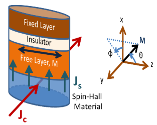
Fig. 1 shows a schematic diagram of a spin Hall device. A charge current flows laterally in the spin Hall material layer and a perpendicular spin current through the cross-section of the structure is generated, which can exert spin-torque on the free layer nanomagnet and switch its magnetization. In the conventional STT devices, the charge current gets spin polarized through a fixed layer, however, passing high current during switching of magnetization occasionally damages the thin insulator layer [39]. Hence, the giant spin Hall devices offer a great advantage over the traditional STT devices. Note that the read current, which is small, still needs to be passed perpendicular to the cross-section of the spin Hall devices and hence the fixed layer in a magnetic tunnel junction (MTJ) structure is required to detect the magnetization states of the free layer nanomagnet [42]. By reversing the direction of the charge current, the magnetization of the free layer can be switched in either direction. Since the charge current and the spin current flow though different cross-sections, it is shown that the spin-to-charge current ratio can be greater than one, unlike the case of traditional STT devices [39]. Both the Oersted field generated by the current and Rashba field are neglected since experimentally it has been verified that they tend to oppose the switching and of small magnitude [39].
Here, we perform an analysis on the energy dissipation in the aforesaid spin Hall devices. Since the charge current flows through the spin Hall material, the Ohmic loss occurs in the spin Hall material itself unlike the case of traditional STT devices, where the energy dissipation incurs in the MTJ stack. The charge current flows laterally through a higher resistance compared to the case if flown perpendicular to the cross-section (of the nanomagnet), however, the MTJ stack (nanomagnets separated by an insulator) has a higher resistance than that of the current flow path in the spin Hall material layer, particularly while using a low-resistivity material for the spin Hall layer. Also, the required charge current is less due to higher spin-to-charge conversion factor in giant spin Hall devices. We show that the energy dissipation is inversely proportional to the lateral area of the spin Hall devices, but scaling down the lateral dimensions also makes the required spin current to switch the magnetization smaller. We solve stochastic Landau-Lifshitz-Gilbert (LLG) equation [43, 44, 45] of magnetization dynamics to depict a strategy whereby the energy dissipation can be reduced simultaneously with lowering of the switching delay and its variance in the presence of room temperature thermal fluctuations, while scaling down the lateral dimensions.
2 Model
We consider the free layer nanomagnet in the shape of an elliptical cylinder with its elliptical cross section lying on the - plane; the major axis is along the -direction and the minor axis is along the -direction (see Fig. 1). The dimensions along the -, - , and -direction are , , and (), respectively. So the lateral area of the spin Hall device is and the nanomagnet’s volume is . In standard spherical coordinate system, is the polar angle and the is the azimuthal angle. Due to shape anisotropy, the two degenerate magnetization states along the -direction ( and ) can store a binary bit of information. The -axis is the in-plane hard axis and -axis is the out-of-plane hard axis. We can write the shape anisotropy energy of the nanomagnet as follows:
| (1) |
where , is permeability of free space, is the saturation magnetization, is the Stoner-Wohlfarth switching field [46], is the out-of-plane demagnetization field [46], and is the mth () component of the demagnetization factor [47] (). The shape anisotropic energy barrier between the two stable magnetization states can be expressed from Equation (1) [putting ] as
| (2) |
The magnetization M of the nanomagnet has a constant magnitude but a variable direction, and hence we can represent it by a vector of unit norm , where is the unit vector in the radial direction in spherical coordinate system represented by (,,); the other two unit vectors in the spherical coordinate system are and for and rotations, respectively.
The effective field and torque acting on the magnetization due to gradient of potential landscape can be expressed as and , respectively.
| (3) |
where
| (4) | |||||
| (5) |
Passage of a spin current in the -direction with spin polarization along the -direction generates a spin-transfer-torque that is given by [4]
| (6) |
where is the spin angular momentum deposition per unit time, the unit vector is in the direction of spin polarization since we want to rotate magnetization from -axis to -axis, and we have used the identity . No asymmetry in spin-transfer-torque switching or field-like torque is considered here [48, 49, 56].
The random thermal fluctuations are incorporated via a random magnetic field , where () are the three components of the random thermal field in Cartesian coordinates. We assume the same properties of the random field as described in Ref. [45]. The random thermal field can be written as [45]
| (7) |
where is the phenomenological dimensionless Gilbert damping parameter, is the Boltzmann constant, is temperature, is the gyromagnetic ratio for electrons and its magnitude is equal to (rad.m).(A.s)-1, is the simulation time-step used, and the quantity is a Gaussian distribution with zero mean and unit variance.
The thermal field and the corresponding torque acting on the magnetization can be written as and , respectively, where
| (8) | |||||
| (9) |
The magnetization dynamics under the action of the torques , , and is described by the stochastic Landau-Lifshitz-Gilbert (LLG) equation [43, 44, 45] as follows.
| (10) |
From the above equation, we get the following coupled equations of magnetization dynamics for and :
| (11) | |||||
| (12) | |||||
We solve the above two coupled equations numerically to track the trajectory of magnetization over time.
The energy dissipated in the nanomagnet due to Gilbert damping can be expressed as , where is the switching delay and is the power dissipated at time given by
| (13) |
Thermal field with zero mean does not cause any net energy dissipation but it causes variability in the energy dissipation by scuttling the trajectory of magnetization.
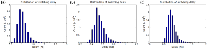
If the magnetization situates exactly along the easy axis, i.e., ( or ), the torque acting on the magnetization given by Equations (3) and (6) becomes zero. That is why only thermal fluctuations can deflect the magnetization vector exactly from the easy axis. Magnetization fluctuates around an easy axis due to thermal agitations and hence we get a distribution of the initial angles (). We consider this initial distribution when magnetization starts switching from . We perform a moderately large number (10,000) of simulations in the presence of thermal fluctuations and when the final value becomes (note that the mean value of is ), the switching is deemed to have completed. Then, the mean and standard deviation of switching delay distribution ( and , respectively), and the mean of energy dissipation are extracted from the simulations. (See Fig. 2 and Table 1 later.)
The energy dissipation due to Gilbert damping is of the order of the energy barrier height, however, the major part of the energy dissipation occurs due to Ohmic loss in the spin Hall material since the charge current flows through it in the -direction (see Fig. 1). The spin-current flows in the -direction, and the ratio of the spin-to-charge current can be expressed as
| (14) |
where () is the spin (charge) current density, () is the area through which spin (charge) current flows, is the spin Hall angle of the spin Hall material used, and is the thickness of the spin Hall material layer. The geometric factor can be selected much greater than one and hence, having can make .
The power dissipation in the spin Hall material can be expressed as
| (15) | |||||
where is the resistivity of the spin Hall material and is the resistance of the spin Hall material layer. The energy dissipation in the spin Hall material layer can be expressed as
| (16) |
where is the time-period until which the charge current is kept active.
3 Results
For the free layer nanomagnet, we consider the widely-used material CoFeB, which has low saturation magnetization A/m [50] and a low Gilbert damping parameter = 0.01. Note that the damping parameter can be modified depending on the adjacent spin Hall material layer due to spin pumping [51]. We choose CuBi as the spin Hall material since it has the lowest factor (=10 -, =–0.24 measured at 10 K [41]) among the other materials utilized in current experiments with an eye to reduce the energy dissipation [see Equation (16)]. We can also possibly utilize platinum as the spin Hall material layer that has - [36], =0.07 [38] measured at room temperature, however, it will incur an energy dissipation of one order more than that of CuBi. Note that platinum increases magnetization damping (i.e., increases the minimum switching current) of CoFeB considerably and the damping parameter is about three times compared to when tantalum is utilized [39].
Note that CoFeB has a resistivity of 100 - [52], which is 10 times more than that of CuBi spin Hall material layer. Hence the current shunting effect [53, 54] through the CoFeB layer is ignored. Therefore, the purpose of utilizing a low-resistive spin Hall material layer is also to tackle the issue of current shunting effect, apart from reducing the energy dissipation. We do need to consider the current shunting effect while utilizing tantalum or tungsten as the spin Hall material layer since they have the resistivity of the same order as of CoFeB [39, 40]. We consider here in-plane switching of magnetization, however, perpendicular switching of magnetization has been demonstrated [16, 55, 56, 39] and can be considered too, particularly to scale down the lateral area of the devices further.
We use both the thicknesses and as 2 nm. We vary the lateral dimensions and of the nanomagnet for different cases considered and we choose the dimensions of the nanomagnet so that it has a single ferromagnetic domain [57, 47]. We always keep the energy barrier = 0.8 eV or 32 at room temperature (=300 K). Following Boltzmann distribution, this means that the error probability due to spontaneous reversal of magnetization is or , which is low enough for application purposes. We can choose a higher barrier height leading to even lower error probability depending on the application requirements. We will now go through the following three cases.
| Case | Nanomagnet size | |||||||||
|---|---|---|---|---|---|---|---|---|---|---|
| (nm3) | (mA) | (mA) | () | (ns) | (ns) | (aJ) | (ns) | (nW) | (aJ) | |
| (a) | 150 100 2 | 1.6000 | 0.1333 | 21.22 | 1.03 | 0.21 | 0.0883 | 2.5 | 377 | 943 |
| (b) | 100 30 2 | 0.7155 | 0.1988 | 9.55 | 0.55 | 0.10 | 0.0395 | 1.2 | 377 | 453 |
| (c) | 100 30 2 | 0.4800 | 0.1333 | 9.55 | 0.78 | 0.15 | 0.0485 | 2.0 | 170 | 204 |
Case (a): We consider a nanomagnet with dimensions = 150 nm, = 100 nm, and = 2 nm. We solve stochastic LLG for 10,000 times and find that it requires about = 1.6 mA to switch always successfully, while the switching current is kept active for 2.5 ns. The corresponding charge current is = 133.3 A. The demagnetization factor () = (0.9468, 0.0339, 0.019) [47], T, and T. The switching delay distribution is plotted in the Fig. 2(a). The mean of switching delay and its standard deviation are 1.03 ns and 0.21 ns, respectively. The major energy dissipation is due to Ohmic loss in the spin Hall material and it turns out to be 943 aJ [see Table 1].
Case (b): We now reduce the lateral dimensions of the nanomagnet and choose the lateral dimensions to be = 100 nm, = 30 nm with an eye to increase the device density on a chip. The thickness is kept same as for the case (a). Hence, both the lateral area and the volume decrease by a factor of 5. Note that the energy barrier between the two stable states is kept constant [see Equation (2)] at this reduced volume by choosing the elliptical cross-section more anisotropic. The demagnetization factor () = (0.8829, 0.0953, 0.0218) [47], T, and T. The anisotropic field increases due to the modification of demagnetization factors at the chosen dimensions [47]. However, at a reduced volume, the magnetization becomes more prone to thermal fluctuations [see Equation (7)]. But the STT switching current also mitigates the detrimental effects of thermal agitations. Since in this case the current needs to switch a nanomagnet of a smaller volume [see Equations (11) and (12)], we show that it is possible to adjust the switching current such that in overall, we can achieve a better performance metrics for both switching delay and energy dissipation at this reduced volume.
According to the Equation (15), we scale down by a factor of to keep the power dissipation constant. The corresponding distribution of switching delay is shown in the Fig. 2(b). Note that both the mean and standard deviation of switching delay have got reduced by half compared to the case (a). The switching current is kept on until 1.2 ns and hence the energy dissipation is reduced by more than half compared to the case (a). Note that even if the spin current is reduced, the charge current required in this case has got increased compared to the case (a) due to the decrease in minor axis of the elliptical cross-section of the nanomagnet [see Equation (14)]. Next we consider another case where the spin current is reduced further to keep the charge current same compared to the case (a).
Case (c): We choose the same dimensions of the nanomagnet as of the case (b) and the same charge current as for the case (a) [see Table 1]. The demagnetization factor, , and are same as of the previous case. The corresponding switching delay distribution is plotted in the Fig. 2(c). Note that both the mean and standard deviation of switching delay distribution have got increased compared to the case (b) due to decrease in , however, the metrics are still much better than that of the case (a) [see Table 1]. The energy dissipation has got reduced by more than half, compared to the case (b), to 204 aJ, which is due to the decrease in spin current .
It should be noted that it is not only the mean of switching delay distribution, but also the standard deviation in switching delay that plays an important role in setting the clock period of magnetization switching for application purposes. A higher standard deviation would lead to setting a higher clock period. In this paper, it is shown that both the mean and the standard deviation of switching delay can be reduced simultaneously, while the lateral area of the giant spin Hall devices is scaled down.
4 Discussions
From Equation (14), it should be noted that the spin diffusion length for spin Hall material is not considered in the expression. For a thick spin Hall material layer (), it does not need to consider . However, we should choose the thickness of the spin Hall material layer small since the charge current (for a required spin current) decreases with the decrease of . It is possible to add a spin-sink layer at the bottom of a thin spin Hall material layer (see Fig. 1) to avoid any backflow of spins. For example, see Ref. [58] for some experimental results, however, research on such front is quite emerging. For CuBi utilized as a spin Hall material layer, such experimental data is not available, however, this concept of adding a spin-sink layer is quite general. Also it should be noted that there is controversy on the experimentally measured spin diffusion length for spin Hall materials [58]. Since for all the three cases in Table 1, the results correspond to the same thickness of the spin Hall material layer, the comparative nature of the analysis is not quite affected. The analysis presented here depicts the necessity of decreasing the thickness of the spin Hall material layer to decrease the charge current and consequently to reduce the energy dissipation.
It is imperative to compare the energy savings utilizing the giant spin Hall effect compared to the traditional way of exerting spin-torque. The energy savings accrue from the decrease in charge current due to the geometric factor and decrease in resistance of the charge flow path compared to the MTJ stack. The reduction of energy dissipation is as high as 3-4 orders of magnitude compared to the conventional spin-transfer-torque switching mechanism [59, 60] and domain-wall racetrack memory [61, 62].
Although the energy dissipation in these giant spin Hall devices has got reduced to the order of 0.1 fJ, the energy dissipation can be further reduced by having a spin Hall material that has even lower factor [see Equation (16)], i.e., having a material with a lower resistivity and a higher spin Hall angle. The target would be the reduction of energy dissipation by a factor of 2 more to be competitive with other emerging technologies [10]. Switching delay and area of a device also need to be competitive with the traditional transistor based technology [63]. The non-volatility of the nanomagnets in these giant spin Hall devices can be utilized to devise a possibly better architecture in terms of performance metrics for application purposes.
5 Conclusions
In conclusion, we have analyzed the energy dissipation in recently proposed spin Hall devices exploiting giant spin Hall effect. After formulating the energy dissipation, we solved stochastic Landau-Lifshitz-Gilbert equation of magnetization dynamics in the presence of room-temperature thermal fluctuations to present a methodology in which both the energy dissipation and switching delay (and its variance) can be reduced simultaneously, while the lateral dimensions of the spin Hall devices are scaled down. The energy dissipation turns out to be of several orders of magnitude less than that of the traditional spin-transfer-torque devices. This field is still emerging and with suitable spin Hall materials, the energy dissipation can be reduced further. This opens up an energy-efficient avenue to control a bit of information in nanomagnetic memory and logic systems for our future information processing paradigm.
References
References
- [1] Wolf S A, Lu J, Stan M R, Chen E and Treger D M 2010 Proc. IEEE 98 2155–2168
- [2] Bader S D and Parkin S S P 2010 Annu. Rev. Condens. Matter Phys. 1 71–88
- [3] Marrows C H and Hickey B J 2011 Phil. Trans. Roy. Soc. A 369 3027–3036
- [4] Sun J Z 2000 Phys. Rev. B 62 570–578
- [5] Ralph D C and Stiles M D 2008 J. Magn. Magn. Mater. 320 1190–1216
- [6] Kalitsov A, Chshiev M, Theodonis I, Kioussis N and Butler W H 2009 Phys. Rev. B 79 174416
- [7] Roy K, Bandyopadhyay S and Atulasimha J 2012 Appl. Phys. Lett. 100 162405
- [8] Zeng Z, Finocchio G and Jiang H 2013 Nanoscale 5 2219
- [9] Chen E, Apalkov D, Diao Z, Driskill-Smith A, Druist D, Lottis D, Nikitin V, Tang X, Watts S, Wang S, Wolf S A, Ghosh A W, Lu J W, Poon S J, Stan M, Butler W H, Gupta S, Mewes C K A, Mewes T and Visscher P B 2010 IEEE Trans. Magn. 46 1873–1878
- [10] Roy K 2013 SPIN 3 1330003 Roy K 2013 Appl. Phys. Lett. 103 173110 Roy K 2014 Appl. Phys. Lett. 104 013103
- [11] Roy K, Bandyopadhyay S and Atulasimha J 2011 Appl. Phys. Lett. 99 063108 Roy K, Bandyopadhyay S and Atulasimha J 2011 Phys. Rev. B 83 224412 Roy K, Bandyopadhyay S and Atulasimha J 2012 J. Appl. Phys. 112 023914 Roy K, Bandyopadhyay S and Atulasimha J 2013 Sci. Rep. 3 3038
- [12] Roy K 2014 J. Phys. D: Appl. Phys. 47 252002
- [13] Liu M, Li S, Zhou Z, Beguhn S, Lou J, Xu F, Lu T J and Sun N X 2012 J. Appl. Phys. 112 063917
- [14] Lei N, Devolder T, Agnus G, Aubert P, Daniel L, Kim J, Zhao W, Trypiniotis T, Cowburn R P, Daniel L, Ravelosona D and Lecoeur P 2013 Nature Commun. 4 1378–1–1378–7
- [15] Duan C G, Velev J P, Sabirianov R F, Zhu Z, Chu J, Jaswal S S and Tsymbal E Y 2008 Phys. Rev. Lett. 101 137201
- [16] Ikeda S, Miura K, Yamamoto H, Mizunuma K, Gan H D, Endo M, Kanai S, Hayakawa J, Matsukura F and Ohno H 2010 Nature Mater. 9 721–724
- [17] Amiri P K and Wang K L 2012 SPIN 2 1240002
- [18] Schmid H 1994 Ferroelectrics 162 317–338
- [19] Spaldin N A and Fiebig M 2005 Science 309 391–392
- [20] Khomskii D I 2006 J. Magn. Magn. Mater. 306 1–8
- [21] Ramesh R and Spaldin N A 2007 Nature Mater. 6 21–29
- [22] D’yakonov M I and Perel’ V I 1971 Sov. Phys. JETP Lett. 13 467
- [23] Hirsch J E 1999 Phys. Rev. Lett. 83 1834
- [24] Jungwirth T, Niu Q and MacDonald A H 2002 Phys. Rev. Lett. 88 207208
- [25] Murakami S, Nagaosa N and Zhang S C 2003 Science 301 1348–1351
- [26] Sinova J, Culcer D, Niu Q, Sinitsyn N A, Jungwirth T and MacDonald A H 2004 Phys. Rev. Lett. 92 126603
- [27] Bakun A A, Zakharchenya B P, Rogachev A A, Tkachuk M N and Fleisher V G 1984 Sov. Phys. JETP Lett. 40
- [28] Kato Y K, Myers R C, Gossard A C and Awschalom D D 2004 Science 306 1910–1913
- [29] Wunderlich J, Kaestner B, Sinova J and Jungwirth T 2005 Phys. Rev. Lett. 94 047204
- [30] Valenzuela S O and Tinkham M 2006 Nature 442 176–179
- [31] Hoffmann A 2013 IEEE Trans. Mag. 49 5172–5193
- [32] Guo G Y, Murakami S, Chen T W and Nagaosa N 2008 Phys. Rev. Lett. 100 096401
- [33] Tanaka T, Kontani H, Naito M, Naito T, Hirashima D S, Yamada K and Inoue J 2008 Phys. Rev. B 77 165117
- [34] Morota M, Niimi Y, Ohnishi K, Wei D H, Tanaka T, Kontani H, Kimura T and Otani Y 2011 Phys. Rev. B 83 174405
- [35] Kimura T, Otani Y, Sato T, Takahashi S and Maekawa S 2007 Phys. Rev. Lett. 98 156601
- [36] Ando K, Takahashi S, Harii K, Sasage K, Ieda J, Maekawa S and Saitoh E 2008 Phys. Rev. Lett. 101 036601
- [37] Mosendz O, Pearson J E, Fradin F Y, Bauer G E W, Bader S D and Hoffmann A 2010 Phys. Rev. Lett. 104 046601
- [38] Liu L, Moriyama T, Ralph D C and Buhrman R A 2011 Phys. Rev. Lett. 106 036601
- [39] Liu L, Pai C F, Li Y, Tseng H W, Ralph D C and Buhrman R A 2012 Science 336 555–558
- [40] Pai C F, Liu L, Li Y, Tseng H W, Ralph D C and Buhrman R A 2012 Appl. Phys. Lett. 101 122404
- [41] Niimi Y, Kawanishi Y, Wei D H, Deranlot C, Yang H X, Chshiev M, Valet T, Fert A and Otani Y 2012 Phys. Rev. Lett. 109 156602
- [42] Julliere M 1975 Phys. Lett. A 54 225–226 Moodera J S, Kinder L R, Wong T M and Meservey R 1995 Phys. Rev. Lett. 74 3273–3276 Mathon J and Umerski A 2001 Phys. Rev. B 63 220403 Butler W H, Zhang X G, Schulthess T C and MacLaren J M 2001 Phys. Rev. B 63 054416 Parkin S S P, Kaiser C, Panchula A, Rice P M, Hughes B, Samant M G and Yang S H 2004 Nature Mater. 3 862–867 Yuasa S, Nagahama T, Fukushima A, Suzuki Y and Ando K 2004 Nature Mater. 3 868–871 Gallagher W J and Parkin S S P 2006 IBM J. Res. Dev. 50 5–23
- [43] Landau L and Lifshitz E 1935 Phys. Z. Sowjet. 8 101–114
- [44] Gilbert T L 2004 IEEE Trans. Magn. 40 3443–3449
- [45] Brown W F 1963 Phys. Rev. 130 1677–1686
- [46] Chikazumi S 1964 Physics of Magnetism (Wiley New York)
- [47] Beleggia M, Graef M D, Millev Y T, Goode D A and Rowlands G E 2005 J. Phys. D: Appl. Phys. 38 3333–3342
- [48] Kubota H, Fukushima A, Yakushiji K, Nagahama T, Yuasa S, Ando K, Maehara H, Nagamine Y, Tsunekawa K and Djayaprawira D D 2008 Nature Phys. 4 37–41
- [49] Sankey J C, Cui Y T, Sun J Z, Slonczewski J C, Buhrman R A and Ralph D C 2008 Nature Phys. 4 67–71
- [50] Yagami K, Tulapurkar A A, Fukushima A and Suzuki Y 2004 Appl. Phys. Lett. 85 5634–5636
- [51] Jamali M, Klemm A and Wang J P 2013 Appl. Phys. Lett. 103 252409
- [52] Jen S U, Yao Y D, Chen Y T, Wu J M, Lee C C, Tsai T L and Chang Y C 2006 J. Appl. Phys. 99 053701–053701–5
- [53] Nakayama H, Ando K, Harii K, Kajiwara Y, Yoshino T, Uchida K and Saitoh E 2010 IEEE Trans. Mag. 46 2202–2204
- [54] Mosendz O, Vlaminck V, Pearson J E, Fradin F Y, Bauer G E W, Bader S D and Hoffmann A 2010 Phys. Rev. B 82 214403
- [55] Miron I M, Garello K, Gaudin G, Zermatten P J, Costache M V, Auffret S, Bandiera S, Rodmacq B, Schuhl A and Gambardella P 2011 Nature 476 189–193
- [56] Kim J, Sinha J, Hayashi M, Yamanouchi M, Fukami S, Suzuki T, Mitani S and Ohno H 2013 Nature Mater. 12 240–245
- [57] Cowburn R P, Koltsov D K, Adeyeye A O, Welland M E and Tricker D M 1999 Phys. Rev. Lett. 83 1042–1045
- [58] Ulrichs H, Demidov V E, Demokritov S O, Lim W L, Melander J, Ebrahim-Zadeh N and Urazhdin S 2013 Appl. Phys. Lett. 102 132402
- [59] Sun J Z, Gaidis M C, O’Sullivan E J, Joseph E A, Hu G, Abraham D W, Nowak J J, Trouilloud P L, Lu Y and Brown S L 2009 Appl. Phys. Lett. 95 083506
- [60] Zhao H, Lyle A, Zhang Y, Amiri P K, Rowlands G, Zeng Z, Katine J, Jiang H, Galatsis K, Wang K L, Krivorotov I N and Wang J P 2011 J. Appl. Phys. 109 07C720
- [61] Parkin S S P, Hayashi M and Thomas L 2008 Science 320 190
- [62] Fukami S, Suzuki T, Nagahara K, Ohshima N, Ozaki Y, Saito S, Nebashi R, Sakimura N, Honjo H, Mori K, Igarashi C, Miura S, Ishiwata N and Sugibayashi T 2009 Low-current perpendicular domain wall motion cell for scalable high-speed MRAM VLSI Technology, 2009 Symposium on (IEEE) pp 230–231
- [63] http://www.itrs.net