Area-Delay-Energy Tradeoffs of Strain-Mediated
Multiferroic Devices
Abstract
Multiferroic devices hold profound promise for ultra-low energy computing in beyond Moore’s law era. The magnetization of a magnetostrictive shape-anisotropic single-domain nanomagnet strain-coupled with a piezoelectric layer in a multiferroic composite structure can be switched between its two stable states (separated by an energy barrier) with a tiny amount of voltage via converse magnetoelectric effect. With appropriate choice of materials, the magnetization can be switched with a few tens of millivolts of voltages in sub-nanosecond switching delay while spending a miniscule amount of energy of 1 attojoule at room-temperature. Here, we analyze the area-delay-energy trade-offs of these multiferroic devices by solving stochastic Landau-Lifshitz-Gilbert equation in the presence of room-temperature thermal fluctuations. We particularly put attention on scaling down the lateral area of the magnetostrictive nanomagnet that can increase the device density on a chip. We show that the vertical thickness of the nanomagnet can be increased while scaling down the lateral area and keeping the assumption of single-domain limit valid. This has important consequence since it helps to some extent preventing the deterioration of the induced stress-anisotropy energy in the magnetostrictive nanomagnet, which is proportional to the nanomagnet’s volume. The results show that if we scale down the lateral area, the switching delay increases while energy dissipation decreases. Avenues available to decrease the switching delay while still reducing the energy dissipation are discussed.
Index Terms:
Nanoelectronics, spintronics, multiferroics, energy-efficient computing, straintronics, area-delay-energy trade-offs.I Introduction
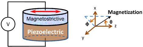
Strain-mediated multiferroic devices, i.e., a magnetostrictive layer strain-coupled to a piezoelectric layer works according to the principles of converse magnetoelectric effect [1, 2, 3, 4, 5]. When a voltage is applied across such heterostructure, the piezoelectric layer gets strained and the strain is transferred elastically to the magnetostrictive layer and generates a stress-anisotropy (or magnetoelastic anisotropy) in it. If we consider a shape-anisotropic single-domain nanomagnet having two stable magnetization states as the magnetostrictive layer, the generated stress-anisotropy can overcome the shape-anisotropy energy barrier and rotate the magnetization. (See Fig. 1.) With appropriate choice of materials, the magnetization can be switched between its two stable states separated by an energy barrier in sub-nanosecond switching delay while expending miniscule amount of energy of 1 attojoule at room-temperature [2, 6]. Such study has opened up a new field called straintronics [1, 7, 8], which can possibly replace the conventional charge-based electronics as our future information processing paradigm. Experimental efforts demonstrating such electric field induced strain-mediated magnetization rotation are emerging too [9, 10, 11, 12, 13]. It should be emphasized that remedies for substrate clamping effect particularly for low-thickness piezoelectric layers ( 100 nm) need to be considered [14, 15]. The use of thin films rather than thick substrates [16] for piezoelectric layers allows us to work with lower voltages and therefore it decreases the energy dissipation.
The stress-anisotropy induced in the magnetostrictive nanomagnet is proportional to the magnetostrictive coefficient of the material used, the generated stress (which is in turn proportional to the electric field), and the volume of the nanomagnet. For a given material with a certain magnetostrictive coefficient and a fixed volume, a higher stress facilitates having a faster switching speed (for a sufficiently fast ramp rate of stress) but causes a higher energy dissipation [6]. The energy dissipation in these multiferroic devices comprises of two components: one is due to magnetization damping through which magnetization relaxes to a minimum energy position dissipating energy and the energy dissipation in the external circuitry due to applied voltage (, where is the capacitance of the piezoelectric layer and is the applied voltage) [2, 6]. Since the voltage required to switch the magnetization is miniscule, the “” energy dissipation is also miniscule.
In this paper, we study the area-delay-energy trade-offs of such multiferroic magnetoelectric devices. We particularly analyze the effect of reducing lateral area to scale down the area consumption on a chip. Scaling down lateral area for a constant thickness reduces both the shape-anisotropic energy barrier height separating the two stable magnetization states and the generated stress-anisotropy in the nanomagnet since they are both proportional to the volume of the nanomagnet. Apparently, the concern is how to deal with such scenario if we wish to decrease the lateral area of such devices. It turns out that while we reduce the lateral area, we can increase the vertical thickness of the nanomagnet to some extent keeping the single-domain limit assumption for the nanomagnet intact. Increasing thickness while reducing lateral area of the nanomagnet facilitates preventing a drastic reduction in volume and hence the induced stress-anisotropy in the nanomagnet does not deteriorate much. Note that we need to keep the shape-anisotropic energy barrier constant since that determines the error-probability of spontaneous reversal of magnetization between two stable states. The decrease in shape-anisotropic energy due to decrease in volume needs to be compensated by properly adjusting the lateral dimensions. We perform simulations using stochastic Landau-Lifshitz-Gilbert (LLG) equation of magnetization dynamics [17, 18, 19] to extract the switching delay and energy dissipation during magnetization reversal.
If we increase the thickness of the nanomagnet, the thickness of the piezoelectric layer needs to be also proportionately increased since the effectiveness of strain-transfer depends on the ratio of the two layers [2]. Modeling the piezoelectric layer as a parallel-plate capacitor and noting that the area, of the capacitor decreases while the thickness increases, the capacitance of the piezoelectric layer () decreases significantly. The lateral area decreases more compared to the increase in thickness of the piezoelectric layer to enforce the single-domain limit, i.e., the factor eventually decreases. Thus even if we increase the voltage for a thicker device to keep a constant electric field (and thus a constant stress) across the device, the “” energy dissipation eventually decreases.
The rest of the paper is organized as follows. Section II describes the model utilized to perform the simulations. Stochastic Landau-Lifshitz-Gilbert (LLG) equation in the presence of room-temperature thermal fluctuations is solved to trace the magnetization dynamics and calculate the associated performance metrics, i.e., switching delay and energy dissipation. Simulation results showing how the performance metrics area, switching delay, and energy dissipation vary with the decrease in lateral dimensions (and the increase in thickness) of the nanomagnet are presented in Section III. Finally, Section IV discusses on the results presented and concludes the paper.
II Model
We model the piezoelectric and magnetostrictive layers as elliptical cylinders as shown in Fig. 1. The magnetostrictive nanomagnet lies on the - plane; the major axis is aligned along the -direction and the minor axis along the -direction. The dimensions of the major axis, the minor axis, and the thickness are , , and , respectively. So the nanomagnet’s aspect ratio is , cross-sectional area is , and volume is . The -axis is the easy axis, the -axis is the in-plane hard axis, and the -axis is the out-of-plane hard axis. Since , the out-of-plane hard axis is much harder than the in-plane hard axis. As becomes higher and the lateral dimensions and become smaller, it is easier for magnetization to deflect out-of-plane. In standard spherical coordinate system, is the polar angle and is the azimuthal angle of the magnetization vector. Note that when = , the magnetization vector lies on the plane of the nanomagnet. Any deviation from = corresponds to out-of-plane excursion.
We can write the total energy of the magnetostrictive polycrystalline single-domain nanomagnet when it is subjected to uniaxial stress along the easy axis (major axis of the ellipse) as the sum of the shape-anisotropy energy and the stress-anisotropy energy [20, 2, 6] as
| (1) |
where
| (2a) | ||||
| (2b) | ||||
| (2c) | ||||
| (2d) | ||||
is the saturation magnetization, is the component of demagnetization factor along -direction, which depends on the nanomagnet’s dimensions [20, 21], is the magnetostrictive coefficient of the single-domain magnetostrictive nanomagnet [20], and is the stress on the nanomagnet. Note that the potential landscape of the magnetostrictive nanomagnet is symmetric in space, however, the out-of-plane excursion of magnetization provides an equivalent asymmetry to facilitate switching of magnetization towards its correct direction when it reaches the - plane () [22]. Thermal fluctuations create an wide distribution of magnetization while switching starts and also the time required to reach is a distribution due to thermal fluctuations [22]. Therefore, it necessitates a sensing methodology to detect when magnetization reaches around but the sensing does not need to be very accurate as intrinsic dynamics provides some tolerance [22]. Note that the product of magnetostrictive coefficient and stress needs to be negative in sign for stress-anisotropy to overcome the shape-anisotropy.
From (1), the in-plane barrier height (i.e., when , , and ) between two magnetization stable states ( and ) can be written as
| (3) |
The probability of spontaneous reversal of magnetization due to thermal fluctuations is according to the Boltzmann distribution, where is the Boltzmann constant, and is temperature. The minimum stress required to overcome the barrier height can be determined as
| (4) |
The minimum stress does not directly depend on volume since both shape-anisotropy and stress-anisotropy energies are proportional to volume, however, depends on the particular dimensions of the nanomagnet (i.e., , , and ) through the dependence of demagnetization factors and . It should be emphasized that the barrier height depends on volume and to satisfy single-domain limit [21], there are certain dimensions of the nanomagnet that we can choose.
The magnetization M of the nanomagnet has a constant magnitude but a variable direction, so that we can represent it by a vector of unit norm where is the unit vector in the radial direction in spherical coordinate system represented by (,,). The torque, acting on the magnetization due to shape and stress-anisotropy is derived from the derivative of potential energy as in (1) [2, 6]. There is an additional torque, due to room-temperature (300 K) thermal fluctuations [6].
The magnetization dynamics under the two aforesaid torques is described by the stochastic Landau-Lifshitz-Gilbert (LLG) equation [17, 18, 19] as
| (5) |
where is the phenomenological damping parameter, is the gyromagnetic ratio for electrons, and .
After solving the LLG equation, we get the following coupled equations for the dynamics of and [6]
| (6) |
| (7) |
where
| (8a) | ||||
| (8b) | ||||
| (8c) | ||||
| (8d) | ||||
is proportional to the attempt frequency of the thermal field, is the simulation time-step, and is a Gaussian distribution with zero mean and unit variance [23].
III Simulation Results
We consider the magnetostrictive layer to be made of polycrystalline Terfenol-D, which has the following material properties – magnetostrictive coefficient (): +9010-5, Young’s modulus (Y): 80 GPa, saturation magnetization (): 8105 A/m, and Gilbert’s damping constant (): 0.1 (Refs. [24, 25, 26, 27]). We use Terfenol-D (TbDyFe), a specially designed composite material rather than common magnetic materials (e.g., iron, nickel, or cobalt) since Terfenol-D has 30 times higher magnetostrictive coefficient in magnitude [2]. Another good choice may be FeGa alloy, which has magnetostrictive coefficient +1510-5 [28]. Since Terfenol-D has positive magnetostrictive coefficient, a compressive stress is required for magnetization to switch [1]. In our convention, a tensile stress is positive and a compressive stress is negative.
The piezoelectric layer is considered to be made of lead-zirconate-titanate (PZT), which has a dielectric constant of 1000 [1]. The PZT layer is assumed to be four times thicker than the magnetostrictive layer so that any strain generated in it is transferred almost completely to the magnetostrictive layer [1]. The maximum strain on the PZT layer is considered to be 500 ppm [29, 30] and it would require an electric field of 2.78 MV/m because =1.810-10 m/V for PZT [31]. (We can also use relaxor ferroelectrics for the piezoelectric layer e.g., PMN-PT, PZN-PT that have high piezoelectric coefficients and generate anisotropic strain, hence it can decrease the electric field further [32, 9, 12].) The corresponding stress in Terfenol-D is the product of the generated strain () and the Young’s modulus (80 GPa). Hence, 40 MPa is the maximum stress that can be generated in the Terfenol-D nanomagnet. For example, to generate 30 MPa stress, it would require voltages of 83.3 mV and 50 mV for nanomagnets with thicknesses 10 nm and 6 nm, respectively.
We always ensure that the magnetostrictive nanomagnet has a single ferromagnetic domain [21, 33] for varied thickness and aspect ratio. The performance metrics switching delay and energy dissipation are determined by solving stochastic Landau-Lifshitz-Gilbert equation in the presence of room-temperature (300 K) thermal fluctuations following the prescription in Ref. [6, 34]. We assume a 50 ps ramp for stress on the magnetostrictive nanomagnet [6].
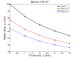
III-A Lateral Dimensions and Demagnetization Factors
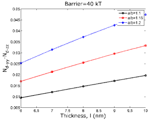
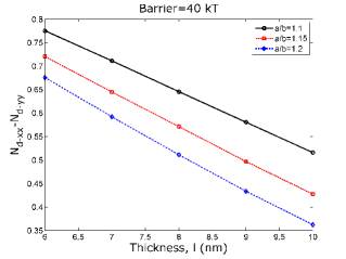
Fig. 2 plots the major axis of the nanomagnet versus its thickness with aspect ratio as a parameter for an energy barrier height of 40 at room-temperature. The decrease in lateral dimensions with the increase in thickness are adjusted to satisfy the single-domain limit assumption [21]. With these dimensions, the demagnetization factors and both increase with thickness and aspect ratio, however, has the opposite trend [21]. Fig. 2 plots the difference , which increases with both thickness and aspect ratio. Fig. 2 plots , which decreases with the increase of both thickness and aspect ratio.
III-B Critical Stress and Success Rate of Switching
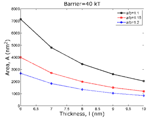
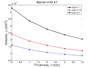
Figs. 3 and 3 show the trend in lateral area and volume of the nanomagnet while varying its thickness with aspect ratio as a parameter. These plots can be derived from the Fig. 2. The decrease in lateral area bodes well with the requirement of scaling down the device size to enhance device density on a chip. However, the decrease in volume has to be compensated by increasing the in-plane shape-anisotropy ( ) to keep the energy barrier height same as 40 (see (3)). Thus, the curves in Fig. 2 show the opposite trend to that of Fig. 3 with the thickness and aspect ratio.
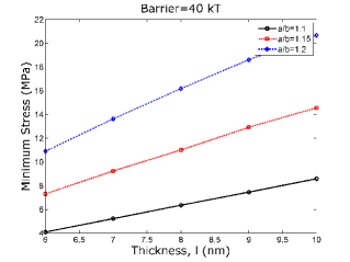
Fig. 3 shows the minimum stress required for stress-anisotropy to overcome the shape-anisotropy energy barrier of the nanomagnet. Since both the anisotropies are proportional to volume, is independent of volume but it is proportional to for a fixed barrier height of 40 (see (4) and Fig. 2).
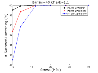
Fig. 4 plots the successful switching rate versus stress for different thicknesses of the nanomagnet. A higher stress keeps the magnetization more out-of-plane (-direction) and thus it is conducive to a higher success rate of switching [22]. For a fixed aspect ratio, a higher thickness of the nanomagnet corresponds to lower volume and thus lesser stress-anisotropy is produced at lower stress levels. This is the reason behind having lower success rate of switching with increasing thickness at the low stress levels.
III-C Switching Delay and Energy Dissipation
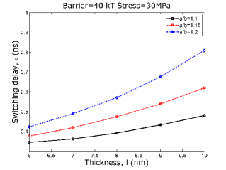
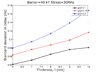
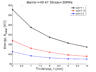
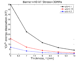
Figs. 5 and 6 plot the metrics switching delay and energy dissipation versus thickness with aspect ratio as a parameter for stress 30 MPa and an energy barrier height of 40 at room-temperature. In Fig. 5, we see that both the mean and standard deviation of switching delay become higher with increasing thickness. The reason behind the increase in switching delay is that it requires a minimum stress to overcome the energy barrier; increases with thickness (see Fig. 3) and hence for a fixed stress of 30 MPa, the torque acting on the magnetization becomes lesser with higher thicknesses. The standard deviation in switching delay increases due to the decrease of nanomagnet’s volume with the increasing thickness (see Fig. 3), which makes magnetization more prone to thermal fluctuations (see (8d)). The energy dissipation curves show an opposite trend because of the delay-energy trade-off. The “” energy dissipation as shown in Fig. 6 decreases with increasing thickness as explained in the Section I.
IV Discussions and Conclusions
We have analyzed the area-delay-energy trade-offs of strain-coupled multiferroic composite devices. It turns out that it is possible to increase the thickness of the magnetostrictive nanomagnet while reducing the lateral area of the nanomagnet keeping the single-domain limit assumption intact. However, the resultant volume of the nanomagnet eventually decreases with the decrease of lateral area. This weakens the induced stress-anisotropy in the nanomagnet for a material with fixed magnetostrictive coefficient and a certain stress value. The switching delay increases with the increasing thickness, while energy dissipation follows the opposite trend. An increase of stress can make the switching delay lower, however, there is a limit on stress that we can apply since it is dictated by the dielectric breakdown of the piezoelectric layer and the associated reliability issues. Thus, increasing magnetostrictive coefficient by superior material synthesis may be a solution to decrease switching delay as we reduce the lateral area (and increase the thickness) of a device. For example, using a twice magnetostrictive coefficient of Terfenol-D (see Ref. [35], however, this is for single-crystal case rather than polycrystalline Terfenol-D) for thickness 10 nm, we can reduce the switching delay to the value same as for thickness 6 nm, while achieving around two times reduction in energy dissipation. Both reducing lateral dimensions and increasing magnetostrictive coefficient are challenging in fabrication and material synthesis procedures, which can increase the device density on a chip.
Note that it may be possible to devise different switching methodologies with strain-mediated multiferroic composites having better performance metrics particularly reducing the lateral area of the devices further. However, since the strain generated is proportional to volume and with scaling volume reduces, it may be very useful to go beyond volumetric effect and employ surface-related phenomena for magnetoelectric coupling [36, 37].
With the growing experimental efforts, such devices may be a staple of modern non-volatile logic and memory systems for our future information processing paradigm and also could be deemed suitable for energy harvesting applications.
Appendix A Fluctuations of Magnetization around Easy Axis due to Thermal Agitations
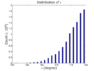
Magnetization in a nanomagnet cannot move exactly from the easy axes () because the torque acting on magnetization become zero at these points [22]. Fortunately, thermal fluctuations can deflect magnetization from these positions. Fig. 7 shows the distribution of polar angle when magnetization is fluctuating around the easy axis for an energy barrier height of 40 and for a nanomagnet with 10 nm thickness and aspect ratio of 1.1. Similar Boltzmann distributions are achieved for different dimensions of the nanomagnet but for same barrier height 40 . The mean of this distribution is used as the magnetization’s initial polar angle to start with.
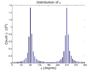
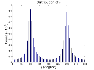
Fig. 8 shows the distribution of azimuthal angle when magnetization is fluctuating around the easy axis for an energy barrier height of 40 . Two cases corresponding to two different thicknesses of the nanomagnet (6 nm and 10 nm) are considered. The distributions are Gaussian peaked with the peaks on the plane of the nanomagnet (). We have assumed the initial value of as , however, assuming the other in-plane angle of magnetization produces similar magnetization dynamics due to symmetry of the underlying equations. Note that the distribution corresponding to the 10 nm thickness one is less peaked since it is easier for the magnetization to deflect out-of-plane with higher thickness ( is decreased at higher thickness, see Fig. 2).
| a | ||||||||||||
|---|---|---|---|---|---|---|---|---|---|---|---|---|
| (nm) | (nm) | (nm2) | (nm3) | (MPa) | (%) | (ns) | (ns) | (kT) | (kT) | |||
| 6 | 1.10 | 100.0 | 0.0095 | 0.7754 | 7139.98 | 42839.90 | 4.25 | 100.00 | 0.35 | 0.042 | 328.45 | 49.85 |
| 1.15 | 76.5 | 0.0170 | 0.7206 | 3996.82 | 23980.94 | 7.60 | 100.00 | 0.38 | 0.063 | 169.95 | 15.66 | |
| 1.20 | 64.0 | 0.0253 | 0.6756 | 2680.83 | 16084.95 | 11.32 | 100.00 | 0.42 | 0.080 | 113.40 | 7.05 | |
| 7 | 1.10 | 82.0 | 0.0121 | 0.7112 | 4800.92 | 33606.47 | 5.41 | 100.00 | 0.36 | 0.051 | 237.05 | 22.59 |
| 1.15 | 63.0 | 0.0214 | 0.6449 | 2710.65 | 18974.54 | 9.55 | 100.00 | 0.42 | 0.076 | 130.51 | 7.21 | |
| 1.20 | 53.0 | 0.0315 | 0.5921 | 1838.49 | 12869.40 | 14.05 | 100.00 | 0.49 | 0.094 | 92.11 | 3.32 | |
| 8 | 1.10 | 69.5 | 0.0147 | 0.6456 | 3448.79 | 27590.32 | 6.57 | 100.00 | 0.39 | 0.065 | 186.85 | 11.67 |
| 1.15 | 54.0 | 0.0255 | 0.5712 | 1991.50 | 15931.97 | 11.41 | 100.00 | 0.47 | 0.087 | 110.15 | 3.89 | |
| 1.20 | 45.5 | 0.0372 | 0.5112 | 1354.98 | 10839.80 | 16.63 | 100.00 | 0.57 | 0.114 | 81.65 | 1.80 | |
| 9 | 1.10 | 60.5 | 0.0172 | 0.5806 | 2613.41 | 23520.71 | 7.70 | 100.00 | 0.43 | 0.076 | 157.00 | 6.71 |
| 1.15 | 47.0 | 0.0296 | 0.4968 | 1508.65 | 13577.83 | 13.23 | 100.00 | 0.54 | 0.098 | 96.55 | 2.24 | |
| 1.20 | 40.0 | 0.0426 | 0.4335 | 1047.20 | 9424.78 | 19.04 | 99.99 | 0.68 | 0.139 | 76.61 | 1.08 | |
| 10 | 1.10 | 53.5 | 0.0197 | 0.5159 | 2043.64 | 20436.42 | 8.79 | 100.00 | 0.48 | 0.081 | 136.85 | 4.10 |
| 1.15 | 42.0 | 0.0333 | 0.4275 | 1204.73 | 12047.32 | 14.88 | 100.00 | 0.62 | 0.117 | 89.59 | 1.43 | |
| 1.20 | 36.0 | 0.0474 | 0.3620 | 848.23 | 8482.30 | 21.18 | 99.91 | 0.81 | 0.168 | 75.44 | 0.71 |
Appendix B Results in Tabular Format
Table I tabulates the simulation results presented in this paper. Different performance metrics e.g., successful switching rate, switching delay, and energy dissipation are given as a function of thickness with aspect ratio of the elliptical cross-section of the nanomagnet as a parameter. As we scale down the lateral dimensions of the nanomagnet, we can increase the thickness to some extent to keep the single-domain assumption valid. However, the volume still decreases with scaling and the volumetric strain decreases proportionately. Therefore the minimum stress required to topple the energy barrier of the nanomagnet increases. Switching delay (both mean and standard deviation) increases and energy dissipation (both and ‘’ one) decreases as already discussed in the paper.
For a given thickness, with the increase of aspect ratio, the anisotropy increases and it allows us to decrease the lateral area so that the energy barrier height can be kept constant. The volume decreases in turn and the minimum stress increases. Switching delay (both mean and standard deviation) increases and energy dissipation (both and ‘’ one) decreases as already discussed in the paper. For thicknesses of 9 and 10 nm, and aspect ratio of 1.2, we notice some switching failures among the 10000 simulations due the increase in the minimum stress . Note that although the stress on the nanomagnet 30 MPa is higher than , sometimes thermal fluctuations can scuttle the magnetization causing switching failures.
References
- [1] K. Roy, “Ultra-low-energy straintronics using multiferroic composites,” SPIN, vol. 3, no. 2, p. 1330003, 2013.
- [2] K. Roy, S. Bandyopadhyay, and J. Atulasimha, “Hybrid spintronics and straintronics: A magnetic technology for ultra low energy computing and signal processing,” Appl. Phys. Lett., vol. 99, no. 6, p. 063108, 2011.
- [3] N. A. Spaldin and M. Fiebig, “The renaissance of magnetoelectric multiferroics,” Science, vol. 309, no. 5733, pp. 391–392, 2005.
- [4] W. Eerenstein, N. D. Mathur, and J. F. Scott, “Multiferroic and magnetoelectric materials,” Nature, vol. 442, no. 7104, pp. 759–765, 2006.
- [5] C. W. Nan, M. I. Bichurin, S. Dong, D. Viehland, and G. Srinivasan, “Multiferroic magnetoelectric composites: Historical perspective, status, and future directions,” J. Appl. Phys., vol. 103, no. 3, p. 031101, 2008.
- [6] K. Roy, S. Bandyopadhyay, and J. Atulasimha, “Energy dissipation and switching delay in stress-induced switching of multiferroic nanomagnets in the presence of thermal fluctuations,” J. Appl. Phys., vol. 112, no. 2, p. 023914, 2012.
- [7] K. Roy, “Ultra-low-energy non-volatile straintronic computing using single multiferroic composites,” Appl. Phys. Lett., vol. 103, no. 17, p. 173110, 2013.
- [8] ——, “Critical analysis and remedy of switching failures in straintronic logic using bennett clocking in the presence of thermal fluctuations,” Appl. Phys. Lett., vol. 104, no. 1, p. 013103, 2014.
- [9] M. Liu, S. Li, Z. Zhou, S. Beguhn, J. Lou, F. Xu, T. J. Lu, and N. X. Sun, “Electrically induced enormous magnetic anisotropy in Terfenol-D/lead zinc niobate-lead titanate multiferroic heterostructures,” J. Appl. Phys., vol. 112, no. 6, p. 063917, 2012.
- [10] N. Lei, T. Devolder, G. Agnus, P. Aubert, L. Daniel, J. Kim, W. Zhao, T. Trypiniotis, R. P. Cowburn, L. Daniel, D. Ravelosona, and P. Lecoeur, “Strain-controlled magnetic domain wall propagation in hybrid piezoelectric/ferromagnetic structures,” Nature Commun., vol. 4, no. 1378, pp. 1378–1–1378–7, 2013.
- [11] M. Liu, Z. Zhou, T. Nan, B. M. Howe, G. J. Brown, and N. X. Sun, “Voltage tuning of ferromagnetic resonance with bistable magnetization switching in energy-efficient magnetoelectric composites,” Adv. Mater., vol. 25, no. 10, pp. 1435–1439, 2013.
- [12] T. Jin, L. Hao, J. Cao, M. Liu, H. Dang, Y. Wang, D. Wu, J. Bai, and F. Wei, “Electric field control of anisotropy and magnetization switching in CoFe and CoNi thin films for magnetoelectric memory devices,” Appl. Phys. Express, vol. 7, no. 4, p. 043002, 2014.
- [13] Z. Zhou, X. Y. Zhang, T. F. Xie, T. X. Nan, Y. Gao, X. Yang, X. J. Wang, X. Y. He, P. S. Qiu, and N. X. Sun, “Strong non-volatile voltage control of magnetism in magnetic/antiferroelectric magnetoelectric heterostructures,” Appl. Phys. Lett., vol. 104, no. 1, p. 012905, 2014.
- [14] J. Pérez de la Cruz, E. Joanni, P. M. Vilarinho, and A. L. Kholkin, “Thickness effect on the dielectric, ferroelectric, and piezoelectric properties of ferroelectric lead zirconate titanate thin films,” J. Appl. Phys., vol. 108, no. 11, p. 114106, 2010.
-
[15]
A. Chopra, E. Panda, Y. Kim, M. Arredondo, and D. Hesse, “Epitaxial
ferroelectric - thin films on
bottom electrode,” J. Electroceram., pp.
1–5, 2014,
DOI: 10.1007/s10832-014-9936-y. - [16] N. A. Pertsev and H. Kohlstedt, “Magnetic tunnel junction on a ferroelectric substrate,” Appl. Phys. Lett., vol. 95, no. 16, p. 163503, 2009.
- [17] L. Landau and E. Lifshitz, “On the theory of the dispersion of magnetic permeability in ferromagnetic bodies,” Phys. Z. Sowjet., vol. 8, no. 153, pp. 101–114, 1935.
- [18] T. L. Gilbert, “A phenomenological theory of damping in ferromagnetic materials,” IEEE Trans. Magn., vol. 40, no. 6, pp. 3443–3449, 2004.
- [19] W. F. Brown, “Thermal fluctuations of a single-domain particle,” Phys. Rev., vol. 130, no. 5, pp. 1677–1686, 1963.
- [20] S. Chikazumi, Physics of Magnetism. Wiley New York, 1964.
- [21] M. Beleggia, M. D. Graef, Y. T. Millev, D. A. Goode, and G. E. Rowlands, “Demagnetization factors for elliptic cylinders,” J. Phys. D: Appl. Phys., vol. 38, no. 18, pp. 3333–3342, 2005.
- [22] K. Roy, S. Bandyopadhyay, and J. Atulasimha, “Binary switching in a ‘symmetric’ potential landscape,” Sci. Rep., vol. 3, no. 3038, p. 3038, 2013.
- [23] G. Brown, M. A. Novotny, and P. A. Rikvold, “Langevin simulation of thermally activated magnetization reversal in nanoscale pillars,” Phys. Rev. B, vol. 64, no. 13, p. 134422, 2001.
- [24] R. Abbundi and A. E. Clark, “Anomalous thermal expansion and magnetostriction of single crystal ,” IEEE Trans. Magn., vol. 13, no. 5, pp. 1519–1520, 1977.
- [25] K. Ried, M. Schnell, F. Schatz, M. Hirscher, B. Ludescher, W. Sigle, and H. Kronmüller, “Crystallization behaviour and magnetic properties of magnetostrictive TbDyFe films,” Phys. Stat. Sol. (a), vol. 167, no. 1, pp. 195–208, 1998.
- [26] R. Kellogg and A. Flatau, “Experimental investigation of Terfenol-D’s elastic modulus,” J. Intell. Mater. Sys. Struc., vol. 19, no. 5, pp. 583–595, 2007.
- [27] http://www.allmeasures.com/Formulae/static/materials/.
- [28] T. Brintlinger, S. H. Lim, K. H. Baloch, P. Alexander, Y. Qi, J. Barry, J. Melngailis, L. Salamanca-Riba, I. Takeuchi, and J. Cumings, “In situ observation of reversible nanomagnetic switching induced by electric fields,” Nano Lett., vol. 10, no. 4, pp. 1219–1223, 2010.
- [29] M. Lisca, L. Pintilie, M. Alexe, and C. M. Teodorescu, “Thickness effect in ferroelectric thin films grown by pulsed laser deposition,” Appl. Surf. Sci., vol. 252, no. 13, pp. 4549–4552, 2006.
- [30] A. J. Masys, W. Ren, G. Yang, and B. K. Mukherjee, “Piezoelectric strain in lead zirconate titante ceramics as a function of electric field, frequency, and dc bias,” J. Appl. Phys., vol. 94, pp. 1155–1162, 2003.
- [31] http://www.memsnet.org/material/leadzirconatetitanatepzt/.
- [32] Y. Jia, S. W. Or, H. L. W. Chan, X. Zhao, and H. Luo, “Converse magnetoelectric effect in laminated composites of PMN-PT single crystal and Terfenol-D alloy,” Appl. Phys. Lett., vol. 88, p. 242902, 2006.
- [33] R. P. Cowburn, D. K. Koltsov, A. O. Adeyeye, M. E. Welland, and D. M. Tricker, “Single-domain circular nanomagnets,” Phys. Rev. Lett., vol. 83, no. 5, pp. 1042–1045, 1999.
- [34] K. Roy, S. Bandyopadhyay, and J. Atulasimha, “Switching dynamics of a magnetostrictive single-domain nanomagnet subjected to stress,” Phys. Rev. B, vol. 83, no. 22, p. 224412, 2011.
- [35] L. Sandlund, M. Fahlander, T. Cedell, A. E. Clark, J. B. Restorff, and M. Wun-Fogle, “Magnetostriction, elastic moduli, and coupling factors of composite Terfenol-D,” J. Appl. Phys., vol. 75, no. 10, pp. 5656–5658, 1994.
- [36] M. Fechner, P. Zahn, S. Ostanin, M. Bibes, and I. Mertig, “Switching magnetization by 180∘ with an electric field,” Phys. Rev. Lett., vol. 108, no. 19, p. 197206, 2012.
- [37] K. Roy, “Electric field-induced magnetization switching in interface-coupled multiferroic heterostructures: a highly-dense, non-volatile, and ultra-low-energy computing paradigm,” J. Phys. D: Appl. Phys., vol. 47, no. 25, p. 252002, 2014.