Edge states and topological insulating phases generated by curving a nanowire with Rashba spin-orbit coupling
Abstract
We prove that curvature effects in low-dimensional nanomaterials can promote the generation of topological states of matter by considering the paradigmatic example of quantum wires with Rashba spin-orbit coupling, which are periodically corrugated at the nanometer scale. The effect of the periodic curvature generally results in the appearance of insulating phases with a corresponding novel butterfly spectrum characterized by the formation of fine measure complex regions of forbidden energies. When the Fermi energy lies in the gaps, the system displays localized end states protected by topology. We further show that for certain corrugation periods the system possesses topologically non-trivial insulating phases at half-filling. Our results suggest that the local curvature and the topology of the electronic states are inextricably intertwined in geometrically deformed nanomaterials.
pacs:
73.63.Nm, 73.21.Cd, 03.65.Vf, 73.43.-fIntroduction –
In recent years, topological non-trivial states of matter have been the subject of growing interest has10 ; moo10 ; qi11 . Topologically non-trivial electronic phases were discovered in time-reversal invariant insulators – leading to the quantum spin Hall (QSH) effect in two-dimensional systems kan05b ; kan05 ; ber06 , and to the existence of protected two-dimensional Dirac cones on the surface of three-dimensional topological insulators fu07b ; hsi08 ; zha09 ; che09 – as well as in insulators with additional specific crystal point group symmetries fu11 . Likewise, topological states in superconducting systems have been intensively studied since their midgap excitations can be potentially used to encode quantum bits with an unusually long coherence time ali12 ; bee13 . Among the different solid-state platforms where topological quantum states of matter are expected to arise, low-dimensional semiconductor nanomaterials play undoubtedly a primary role. The QSH effect, for instance, was first theoretically predicted ber06 and later experimentally proved in HgTe quantum wells kon07 . An heterostructure comprising a semiconductor nanowire with strong spin-orbit coupling and a conventional s-wave superconductor has been suggested to host a topological superconducting phase lut10 ; ore10 with signatures of midgap Majorana bound states already reported mou12 .
Apart from these conventional material geometries, rapid advances in nanostructuring techniques have enabled the synthesis of novel low-dimensional nanostructures in which flexible semiconductor nanomaterials can be bent into curved, deformable objects such as spiral-like nanotubes pri00 ; sch01 , nanohelices zha02 and even complex nanoarchitectures resembling structures that form naturally in the most basic forms of life xu15 . On the one hand, these next-generation nanomaterials carry an enormous potential in electronics, ranging from flexible displays to the integration of semiconductor electronics with the soft, curvilinear surfaces of the human body rog11 ; jo15 . On the other hand, the very fundamental quantum mechanical properties of the charge carriers in these nanomaterials are strongly affected by the curved background in which they live dew57 . Consequently, unique curvature-induced electronic and transport properties have been identified. These include, but are not limited to, the appearance of winding-generated bound states ort10 , and an extremely large anisotropic magnetoresistance in non-magnetic and spin-orbit-free semiconducting rolled-up nanotubes cha14 .
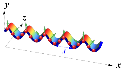
A relevant question that naturally arises is whether and under what circumstances the interplay between curvature effects on the electronic properties and the topology of the ground state of a low-dimensional solid-state system can be significant. In this Letter, we show that not only such interplay is relevant but also that the curved geometry of a bent nanomaterial can promote the generation of non-trivial edge states and topological insulating phases. We prove the assertion above by considering the simple example of a nanowire with Rashba spin-orbit coupling which is corrugated to acquire a ”serpentine”-like planar shape [c.f. Fig. 1]. The ensuing periodic canting of the spin-orbit field axis leads to a miniband structure and a correspondent metal-insulator transition at different filling fractions. This, in turn, leads to a butterfly spectrum that, however, is neither of the Hofstadter type hof76 nor of the Moth type ost05 . A subsequent analysis of the system with open boundary conditions shows the occurrence of midgap edge states, which we show to be topological in nature. Finally, for certain corrugation periods, the system can display topologically non-trivial insulating phases at half-filling.
Metal-insulator transition –
Our starting point is an effective continuum model for a planarly curved quantum wire with a Rashba spin-orbit term originating from an electric field pointing in the direction perpendicular to the plane of the wire (the axis in Fig. 1). In its symmetric, Hermitian, form it reads:
| (1) |
where is the arclength of the bent nanowire measured from a reference point, is the effective mass of the charge carriers, and is the strength of the Rashba spin-orbit coupling. Finally is a local Pauli matrix comoving with the electrons as they propagate along , and explicitly reads , where is the local normal direction of the curved wire, while the ’s are the usual Pauli matrices. The Hamiltonian in Eq. 1 corresponds to the effective continuum model for curved quantum wires of Ref. gen13, in the absence of strain-induced effects, and can be mapped onto the model for a conventional quantum wire with a locally varying spin-orbit field axis [c.f. Fig. 1]. The latter can be determined by writing the normal direction in the Euclidean space in terms of an angle as , and using the Frenet-Serret type equation of motion with the tangential direction and the local curvature. It then follows that the local direction of the spin-orbit field axis is entirely determined by the curvature of the quantum wire via . For a periodically corrugated quantum wire, it also implies that the spin-orbit field axis undergoes a periodic canting with the maximum canting angle proportional to the curvature.
In order to study the effect of such a periodic canting of the spin-orbit field axis on the electronic properties of a quantum wire, we next introduce a tight-binding model obtained by discretizing Eq. 1 on a lattice. It can be written as:
| (2) |
where are operators creating and annihilating, respectively, an electron at the -th site with spin projection along the axis, is the hopping amplitude between nearest-neighbor sites, and the spin-dependent nearest-neighbor hopping amplitudes are
| (3) |
In the equation above, and , which are determined by the position of the atoms along the quantum wire and the specific geometric shape of the nanocorrugation. For the latter, we assume a simple sinusoidal form with parametric equation in Euclidean space with corrugation period and corrugation height . The atomic positions can be instead written as , where and are integers whose ratio ( being the lattice constant) while accounts for non-equivalent displacements of the atoms in one corrugation period. As a result, the local spin-dependent hopping amplitudes render a one-dimensional superlattice with superlattice constant . Although in a quantum wire smoothly corrugated at the tens of nanometers scale, we will extend our analysis to the full range taking Eq. 2 as a general model system to study curvature effects even in microscopically buckled atomic chains.
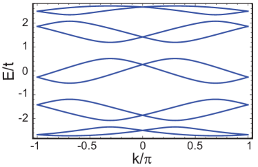
Fig. 2 shows the band structure for in the first mini-Brillouin zone (mBZ) . The presence of the spin-orbit interaction terms removes the spin degeneracy of the minibands except at the time-reversal invariant points where the eigenstates are Kramers degenerate. This, however, does not preclude a priori band gaps opening at different points in the mBZ. And indeed Fig. 2 shows the occurrence of full bandgaps at the filling fractions , with integer, whose magnitude monotonically increases with the corrugation height . We find the opening of bandgaps for finite values of the corrugation height to occur for [see Supplemental Material]. Henceforth, the periodic corrugation of the nanowire generally induces a metal-insulator transition, and thus defines a nanoflex transistor switch, the status of which is “on” when the nanowire is flat and “off” when the nanowire is planarly curved. A similar nanoscale transistor switch has been suggested in nanohelices without spin-orbit coupling but subject to an externally applied rotating electric field qi09 .
Butterfly spectrum and topological edge states –
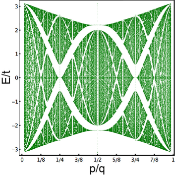
To further verify that the metal-insulator transition is a generic feature due to the periodic canting of the Rashba spin-orbit field axis, we have diagonalized the Hamiltonian Eq. 2 for different commensurate superlattices, changing the displacement field in the interval while keeping the ratio fixed. Fig. 3 shows the ensuing energy spectrum as a function of the ratio between the atomic lattice constant and the corrugation period. It exhibits two main holes of forbidden energies with a double wing shape joining at and . The generation of replicas of such twin wings of holes of finite measure and various sizes, the largest of which join at , evidences a self-similar “butterfly”-like structure of the electronic spectrum. Although a rigorous proof cannot be made, this also reminds one of a fractal structure. Furthermore, the present spectrum is manifestly different in shape both from the Hofstadter butterfly realized in conventional two-dimensional electron gases hof76 , graphene moiré superlattices pon13 and one-dimensional optical superlattices aid13 ; miy13 , as well as from the moth butterfly discussed in the context of cold atoms in non-Abelian gauge potentials ost05 .
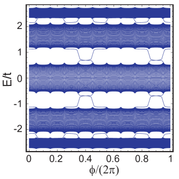
Having established the ubiquitous presence of insulating phases in our nanocorrugated nanowire, we have then analyzed the possible occurrence of localized edge states within the curvature-induced gaps while sweeping the displacement field , as routinely done in one-dimensional optical superlattices with an additional dynamical parameter lan12 ; mar15 . Fig. 4 shows the energy spectrum for a finite size system with open boundary conditions considering the superlattice periods . Within all gaps, there appear edge states localized at the left and right boundaries of the atomic chain whose energy changes continuously with , connecting the valence to the conduction bulk bands. Since the appearance of such edge states can be generally attributed to non-trivial topological properties of bulk systems, we have then analyzed the topological character of the ground state of the system with the displacement field playing the role of an artificial dimension zha13 . It can be shown that the addition of this extra dimension breaks the “time-reversal” symmetry constraint , thereby allowing for insulating phases with non-zero Chern numbers. We have therefore computed the Chern numbers in the insulating phases of Fig. 2 using the method outlined in Ref. tak05, and have found Chern number and for the two central and two exterior gaps respectively. This result is in perfect agreement with the foregoing analysis of the spectrum with open boundary conditions, which, depending on the filling fraction, indeed shows four or eight edge states per edge composed of the two spin species [c.f. Fig. 3]. We have verified that in-gap edge states protected by a non-zero Chern number also appear at different values of [see the Supplemental Material], thereby directly proving the general occurrence of edge states topological in nature in a nanocorrugated quantum wire.
Topological insulating phases –
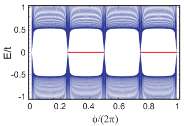
We finally show that a periodic canting of the Rasha spin-orbit field axis can also lead to one-dimensional topological insulating phases. This occurs at the central points of the wings in our butterfly spectrum of Fig. 3. For all values of , the system possesses time-reversal symmetry with as required for spin-one-half fermions, a unitary chiral symmetry , and an antiunitary symplectic particle-hole symmetry with . This also implies that at these selected values, the system is in the chiral symplectic symmetry class CII of the Altland-Zirnbauer classification alt97 , and thus possesses an integer topological invariant provided it is insulating at half-filling. In terms of the displacement field , we find that the half-filling gap has an even number of closing-reopening points [c.f. Fig. 5 and Supplemental Material], which is an unambiguous signal of the occurrence of a topological phase transition between insulating phases with different invariant. To verify this point, we have thus considered a superlattice system with and open boundary conditions. The ensuing energy spectrum as a function of the displacement field is shown in Fig. 5. It shows the presence of two spin-degenerate topologically protected zero-energy modes between the gap closing-reopening points, thereby explicitly proving that the geometric displacement of the atoms in a nanocorrugated nanowire drives a topological phase transition between a and a insulating state. Precisely the same feature is encountered at the central points of the wings replicas in the butterfly spectrum of Fig. 3 [see the Supplemental Material].
Conclusions –
To sum up, we have analyzed curvature effects on the electronic states of a nanocorrugated quantum wire with Rashba spin-orbit interaction. We have shown that the ensuing periodic canting of the Rashba spin-orbit field yields a novel butterfly spectrum with insulating phases characterized by the presence of edge states, which are topological in origin. We have also shown that the curved geometry of such a wrinkled nanowire can promote the onset of one-dimensional topological insulating phases with topologically protected zero end modes. Our results constitute a proof-of-principle demonstration that the geometric curvature of flexible nanomaterials can impact the topology of the electronic states in low-dimensional systems, and can thus inaugurate the search for other topological non-trivial states of matter in solid-state systems manufactured with the most advanced nanotechnology techniques.
Acknowledgements –
We acknowledge the financial support of the Future and Emerging Technologies (FET) programme within the Seventh Framework Programme for Research of the European Commission, under FET-Open grant number: 618083 (CNTQC). CO thanks the Deutsche Forschungsgemeinschaft (grant No. OR 404/1-1) for support.
References
- (1) M. Z. Hasan and C. L. Kane, Rev. Mod. Phys. 82, 3045 (2010).
- (2) J. E. Moore, Nature (London) 464, 194 (2010).
- (3) X.-L. Qi and S.-C. Zhang, Rev. Mod. Phys. 83, 1057 (2011).
- (4) C. L. Kane and E. J. Mele, Phys. Rev. Lett. 95, 146802 (2005).
- (5) C. L. Kane and E. J. Mele, Phys. Rev. Lett. 95, 226801 (2005).
- (6) B. A. Bernevig, T. L. Hughes, and S.-C. Zhang, Science 314, 1757 (2006).
- (7) L. Fu, C. L. Kane, and E. J. Mele, Phys. Rev. Lett. 98, 106803 (2007).
- (8) D. Hsieh, D. Qian, L. Wray, Y. Xia, Y. S. Hor, R. J. Cava, and M. Z. Hasan, Nature 452, 970 (2008).
- (9) H. Zhang, C.-X. Liu, X.-L. Qi, X. Dai, Z. Fang, and S.-C. Zhang, Nat Phys 5, 438 (2009).
- (10) Y. L. Chen, J. G. Analytis, J.-H. Chu, Z. K. Liu, S.-K. Mo, X. L. Qi, H. J. Zhang, D. H. Lu, X. Dai, Z. Fang, S. C. Zhang, I. R. Fisher, Z. Hussain, and Z.-X. Shen, Science 325, 178 (2009).
- (11) L. Fu, Phys. Rev. Lett. 106, 106802 (2011).
- (12) J. Alicea, Reports on Progress in Physics 75, 076501 (2012).
- (13) C. W. J. Beenakker, Annual Review of Condensed Matter Physics 4, 113 (2013).
- (14) M. König, S. Wiedmann, C. Brüne, A. Roth, H. Buhmann, L. W. Molenkamp, X.-L. Qi, and S.-C. Zhang, Science 318, 766 (2007).
- (15) R. M. Lutchyn, J. D. Sau, and S. Das Sarma, Phys. Rev. Lett. 105, 077001 (2010).
- (16) Y. Oreg, G. Refael, and F. von Oppen, Phys. Rev. Lett. 105, 177002 (2010).
- (17) V. Mourik, K. Zuo, S. M. Frolov, S. R. Plissard, E. P. A. M. Bakkers, and L. P. Kouwenhoven, Science 336, 1003 (2012).
- (18) V. Y. Prinz, V. A. Seleznev, A. K. Gutakovsky, A. V. Chehovskiy, V. V. Preobrazhenskii, M. A. Putyato, and T. A. Gavrilova, Physica E (Amsterdam) 6, 828 (2000).
- (19) O. G. Schmidt and K. Eberl, Nature (London)410, 168 (2001).
- (20) H.-F. Zhang, C.-M. Wang, and L.-S. Wang, Nano Letters 2, 941 (2002).
- (21) S. Xu, Z. Yan, K.-I. Jang, W. Huang, H. Fu, J. Kim, Z. Wei, M. Flavin, J. McCracken, R. Wang, A. Badea, Y. Liu, D. Xiao, G. Zhou, J. Lee, H. U. Chung, H. Cheng, W. Ren, A. Banks, X. Li, U. Paik, R. G. Nuzzo, Y. Huang, Y. Zhang, and J. A. Rogers, Science 347, 154 (2015).
- (22) J. A. Rogers, M. G. Lagally, and R. G. Nuzzo, Nature (London) 477, 45 (2011).
- (23) J.-W. Jo, J. Kim, K.-T. Kim, J.-G. Kang, M.-G. Kim, K.-H. Kim, H. Ko, Y.-H. Kim, and S. K. Park, Advanced Materials 27, 1182 (2015).
- (24) B. S. DeWitt, Rev. Mod. Phys. 29, 377 (1957).
- (25) C. Ortix and J. van den Brink, Phys. Rev. B 81, 165419 (2010).
- (26) C.-H. Chang, J. van den Brink, and C. Ortix, Phys. Rev. Lett. 113, 227205 (2014).
- (27) D. R. Hofstadter, Phys. Rev. B 14, 2239 (1976).
- (28) K. Osterloh, M. Baig, L. Santos, P. Zoller, and M. Lewenstein, Phys. Rev. Lett. 95, 010403 (2005).
- (29) P. Gentile, M. Cuoco, and C. Ortix, SPIN 03, 1340002 (2013).
- (30) X.-L. Qi and S.-C. Zhang, Phys. Rev. B 79, 235442 (2009).
- (31) L. A. Ponomarenko, R. V. Gorbachev, G. L. Yu, D. C. Elias, R. Jalil, A. A. Patel, A. Mishchenko, A. S. Mayorov, C. R. Woods, J. R. Wallbank, M. Mucha-Kruczynski, B. A. Piot, M. Potemski, I. V. Grigorieva, K. S. Novoselov, F. Guinea, V. I. Fal’Ko, and A. K. Geim, Nature (London)497, 594 (2013).
- (32) M. Aidelsburger, M. Atala, M. Lohse, J. T. Barreiro, B. Paredes, and I. Bloch, Phys. Rev. Lett. 111, 185301 (2013).
- (33) H. Miyake, G. A. Siviloglou, C. J. Kennedy, W. C. Burton, and W. Ketterle, Phys. Rev. Lett. 111, 185302 (2013).
- (34) L.-J. Lang, X. Cai, and S. Chen, Phys. Rev. Lett. 108, 220401 (2012).
- (35) P. Marra, R. Citro, and C. Ortix, Phys. Rev. B 91, 125411 (2015).
- (36) F. Zhang, C. L. Kane, and E. J. Mele, Phys. Rev. Lett. 111, 056403 (2013).
- (37) T. Fukui, Y. Hatsugai, and H. Suzuki, Journal of the Physical Society of Japan 74, 1674 (2005).
- (38) A. Altland and M. R. Zirnbauer, Phys. Rev. B 55, 1142 (1997).