Far-infrared absorption of undoped and Br-doped carbon nanofiber powder in stacked-cup cone configuration
Abstract
We carried out room-temperature far-infrared (40–650 cm-1) transmission measurements on undoped and bromine-doped powder samples of carbon nanofibers in stacked-cup cone geometry. The transmission spectra of both doped and undoped samples were fit to a Drude-Lorentz model. A single Drude component and a small bandgap (around 8 meV) semiconducting Lorentzian component along with 3 other Lorentz components were essential to get a good fit in the entire measured frequency range. A decreased metallic conductivity along with a red-shift of the lowest semiconducting gap was found after bromine doping. A significant decrease in the scattering rate upon heavy doping has been qualitatively explained as partial ordering of intercalated dopant ions. Absorption spectra were derived from the transmission spectra under the assumption of non-dispersive reflectance. These spectra were compared to Drude-Lorentz model absorption spectra. The free-carrier density of the n-type powder and the electronic mean free path were estimated and compared with previously reported values for single-walled nanotubes and pyrolytic graphite.
I Introduction
Their unique electronic and mechanical properties have caused carbon nanotubes (CNT) to attract much interest among researchers since their discovery.Iijima (1991) CNTs constitute a new class of materials that could contribute to the development of novel nanoscale electronic devices.Ebbesen et al. (1996); Tans et al. (1997); Saito (1997); Chico et al. (1996); Bockrath et al. (1997); Wong et al. (1997); Buongiorno Nardelli et al. (1998) Isolated single-wall nanotubes (SWNT) and bundled nanoropes have been studied extensively and are reported to have either metallic or semiconducting phases, based on their () wrapping vector indices.Dresselhaus et al. (1992); Mintmire et al. (1992); Hamada et al. (1992); Kane and Mele (1997) The related materials, carbon nanofibers (CNF), also known as stacked-cup carbon nanotubes (SCCNT), are bigger in diameter than carbon nanotubes. They are highly graphitic carbon nanomaterials with excellent mechanical properties, electrical and thermal conductivity, all strongly dependent on growth technique and high-temperature heat treatment routine.Bruce and Alyones (2012); Howe et al. (2006); Endo et al. (2003); Tibbetts et al. (2007); Shimamoto et al. (2010); Darmstadt et al. (1998) These properties make them suitable for various applications such as radio frequency interference shields, electrostatic painting, or electrostatic discharge probes. Qualities like better net weight/strength ratio, low processing cost, improved tensile and bending strengths, high specific heat, and high corrosion resistance make them an ideal reinforcing engineered composites for industrial applications.Okuda (1992)
Structural characteristics such as diameter, length, chirality and defects which essentially dictate all important properties in SCCNT and related carbon forms, are difficult to control during synthesis and therefer great interest has been lately observed towards controlling their properties through extrinsic doping methods.Kazaoui et al. (1999); Ruzicka et al. (2000); Duclaux (2002); Gao et al. (1998) The study of doping behavior gets little convoluted because of the mixed metallic and semiconducting phases coexisting in most carbon nanomaterials. Nonetheless, the doping process alters the valence and conduction band statistics and also the free carrier dynamics in these systems, just like it does in graphite hence, it serves as a tool for the tuning of electronic and mechanical properties.Lee et al. (1997); Grigorian et al. (1998) Previous study of bromine intercalation in highly oriented pyrolytic graphite (HOPG) has demonstrated a pathway to weaken the interplanar coupling between individual layers and pushing the system towards an ordered stack of graphene sheets, possibly dominated by Dirac fermions. It has resulted into enhanced carrier density per carbon, higher mobility along the graphite plane and reduced transport along the epitaxial direction due to weakened interplanar coupling.Tongay et al. (2010) Such direct tuning of electronic properties in carbon nanomaterials are highly desirable for their potential electronic applications. Frequency-dependent optical studies of doped and undoped carbon nanomaterials has shown the low-frequency metallic behavior coexisting along with a small bandgap (around 8 meV) semiconducting phase. This gap is attributed either to a secondary gap which is caused by the curvature of certain semi metallic tubes or to symmetry-breaking due to neighboring tubes in metallic phase.Kane and Mele (1997); Delaney et al. (1998); Ouyang et al. (2001) Moreover, the higher frequency range studies have shown the electronic band structure tuning in terms of disappearance and emergence of several new peaks on account of either electron depletion from or electron filling into specific bands of the semiconducting or metallic phases, once p-type (I2, Br2, N2) and n-type (K, Cs, organic radical-anions) dopants were introduced.Kazaoui et al. (1999); Kataura et al. (1999); Rao et al. (1998); Ayala et al. (2010); Ismagilov et al. (2009). This article is mainly focussed on investigating the absorption and conductive properties of carbon nanofibers in the stacked-cup cone configuration through optical measurements and also explores the possibility of tuning these properties through acceptor-like dopant at low and high concentration.
II EXPERIMENTAL PROCEDURES AND RESULTS
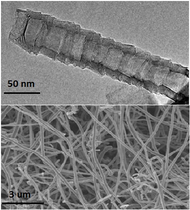
Room-temperature far-infrared transmission measurements were conducted on hollow and cylindrical stacked-cup carbon nanofiber powder samples. High quality samples (Pyrograf III, CNF PR-25-XT-PS) were prepared by Applied Sciences, Inc. It has a unique structure in which the graphene plane surface is canted from the fiber axis exposing the plane edges present on the interior and exterior surfaces of the carbon nanofibers. These nanofibers have diameters ranging between 60–150 nm and lengths varying from tenths to tens of micrometers.Bruce and Alyones (2012) High resolution TEM images shown below in Fig. 1 give details about the structural features of the sample. These fibers were pyrolytically stripped making them free from any CVD carbon and polyaromatic hydrocarbon cantamination on surface.
Transmission spectra were acquired in the far infrared range (40–650 cm-1) using a Bruker 113v Fourier-transform interferometer. A helium-cooled silicon bolometer detector was used in this spectral range. A homogeneous layer of CNF powder of thickness 0.25 mm, 0.15 mm and 0.10 mm were uniformly spread between two polyethylene windows. The sample holder had a 6 mm aperture. Later, the transmission measurements were repeated under identical conditions immediately after exposing the powder samples to Br2 for 10 min and 100 min respectively to study the effect of bromine intercalation. The extent of bromine doping was estimated by observing the change in the density of the sample powder. The density of the undoped sample was estimated to be around 0.3 g/cm3. This density increases to 0.39 g/cm3 after 10 min. of bromine exposure, changing the stoichiometry to CBr0.045. A 100 min. of bromine exposure resulted into a doped powder of CBr0.14 stoichiometry with density around 0.58 g/cm3. The polyethylene windows did introduce interference fringes in the transmission spectra which were removed carefully using a Fourier-transform smoothening technique. The fringe removal process did not change the level of transmission.
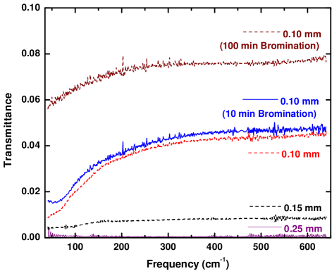
Fig. 2 shows the room temperature transmission spectra of the undoped CNF sample for different thicknesses as well as the spectra after bromination. We observed negligible transmission for the sample thickness of 0.25 mm. The transmission level increases slightly as the thickness decreases to 0.15 mm but is still below 1% in the entire far infrared range. However we observed notable increase in the transmission as thickness is decreased to 0.10 mm. The transmission decreases from about 5% to 1% as frequency decreases from 650 cm-1 to 40 cm-1. The transmission starts decreasing more quickly around 150 cm-1; this behavior can also be seen in the spectra of the 0.15 mm thick sample. All further measurements and analysis were conducted with the 0.10 mm thick powder sample. The transmission measurements were repeated immediately after brominating two powder samples, one for 10 min and one for 100 min. The transmission for 10 min brominated powder sample is quite similar to the undoped sample except for a more obvious onset of increased transmission at low frequencies. In contrast, the transmission of the 100 min brominated sample is substantially increased over the entire range.
III ANALYSIS
III.1 Drude-Lorentz model fits
A Drude-Lorentz model was used to fit the transmission data of the CNF powder sample. Fig. 3 shows the Drude-Lorentz fit to the transmission data. The Drude component characterizes the free carriers and their dynamics at zero frequency whereas the Lorentz contributions are also included to account for the electronic transitions due to both the low gap semiconducting phase of the sample and higher-energy transitions. The dielectric function isWooten (1972)
| (1) |
where the first term represents the core electron contribution (transitions above the measured range, the second term is free carrier contribution characterized by Drude plasma frequency and free carrier relaxation time and the third term is the sum of four Lorentzian oscillators representing the electronic contributions to the dielectric function. The Lorentzian parameters are the th oscillator plasma frequency , its central frequency , and its linewidth . This dielectric function model is used in a least-squares fit to the transmittance data.
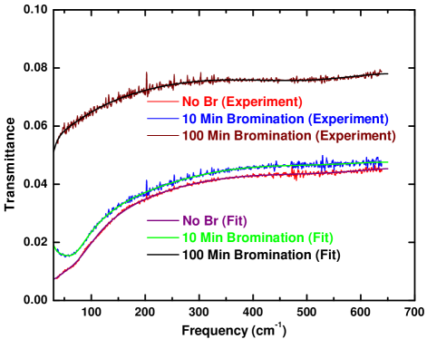
Table 1 contains one Drude term along with 4 other electronic excitation terms. There were no obvious vibrational features observed in any of the samples. All three samples were identified as being in a mixed metallic phase of CNF bundles along with a low-gap semiconducting phase. In many previous studies, this semiconducting gap in CNT around 8 meV has been attributed to either curvature induced gap or due to symmetry-breaking among neighboring tubes in metallic phase.Kane and Mele (1997); Delaney et al. (1998); Ouyang et al. (2001)
III.2 Far-infrared characteristics
Next, the absorption coefficient was computed from the transmission data by invertingWooten (1972)
| (2) |
where is the thickness and is the “single-bounce” reflectance (the reflectance of a single surface). This equation is quadratic in with one positive root
| (3a) | |||
| (3b) |
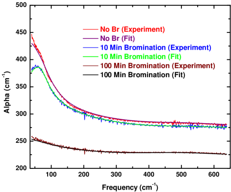
where is the refractive index, taken as a constant with a value of = 4.1. A comparison between the absorption coefficient derived from the transmission spectra using Eq. 3a and calculated absorption coefficient using the set of DL parameters from Table 1 is shown in Fig. 4. It shows an averall decrease in the absorption coefficient with Br-doping in the enire measurement range. That the agreement is good gives us confidence in the fitting procedure and the transmission based absorption coefficient estimation routine.
| Modes | Symbols | No Br | 10 Min. | 100 Min. |
|---|---|---|---|---|
| assignment | (cm-1) | (cm-1) | (cm-1) | |
| Drude component | 73 | 65 | 41 | |
| metallic phase | 33 | 41 | 15 | |
| Low-gap | 30 | 24 | 25 | |
| semiconducting | 69 | 67 | 43 | |
| phase | 80 | 53 | 112 | |
| Electronic | 264 | 262 | 256 | |
| excitation | 137 | 139 | 132 | |
| 2 | 838 | 829 | 850 | |
| Electronic | 110 | 104 | 103 | |
| excitation | 616 | 613 | 613 | |
| 3 | 696 | 672 | 709 | |
| Electronic | 202 | 220 | 186 | |
| excitation | 1098 | 1098 | 1082 | |
| 4 | 562 | 528 | 561 |
We interpret the rise in absorption below 150 cm-1 as due to free-carriers in the powder samples. This is evident in the conductivity spectrum, calculated from the same set of DL parameters and shown in Fig. 5. The real part of the optical conductivity is where represents the imaginary part of the dielectric function in Eq. 1. There is a free carrier absorption rise at the lowest measured frequency which rolls off as the frequency reaches the Drude relaxation rate . A small overlapping absorption shoulder around 50–80 cm-1 can also be observed which is attributed to the low-gap semiconducting component in the CNF powder sample. The optical conductivity, especially the Drude contribution, decreases with increasing bromine intercalation. This change can also be quantitatively seen in Table 1 where the Drude plasma frequency for 100 min. sample drops to almost half of the undoped sample even after the scattering time gets doubled.
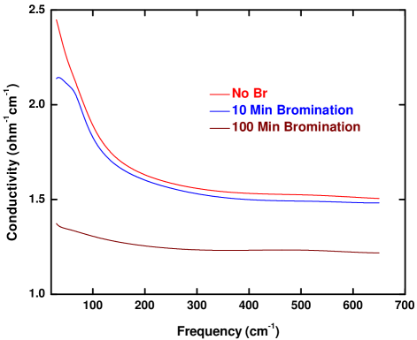
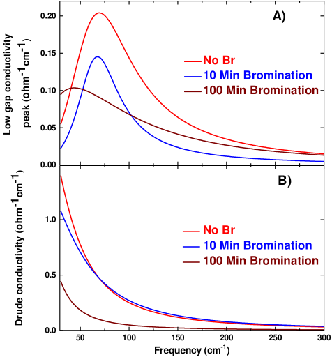
Fig. 6 shows the conductivity contribution from the lowest electronic transition due to the semiconducting phase in panel A) whereas the Drude conductivity from the metallic phase is shown in panel B). The semiconducting gap (around 8 meV for the undoped sample) shifts towards lower frequencies after 100 minute bromination. The strength of this electronic transition also decreases and gets much broader with bromination. As DL parameters suggest, the Drude conductivity decreases with bromination and scattering rate surprisingly drops down significantly for 100 min. sample.
IV DISCUSSION AND CONCLUSIONS
The amphoteric behavior of cabon nanomaterials and changes in their transport properties upon doping has been qualitatively explained in terms of the charge-transfer mechanism in the framework of the rigid band model.Kazaoui et al. (1999) Doping with bromine modifies the structural framework of nanofiber by occupying the endohedral sites or interstitial sites or by substituting carbon from the tube surface and forming heteronanofibers as shown in previous studies.Ayala et al. (2010); Gao et al. (1998); Ismagilov et al. (2009) In highly oriented pyrolytic graphite (HOPG), it is previously shown that transport properties are highly anisotropic which gets even more pronouced upon doping. While a small charge transfer from intercalated bromine atoms enhances the carrier density per carbon and makes the transport along the sheet more metallic, it also suppresses the conductivity along the perpendicular direction by decreasing the tunneling probability between sheets by acting like a negative pressure, pushing them apart.Tongay et al. (2010) Randomly oriented fiber axis in the powder form however, one can only achieve a conductivity which is average over all directions. In a nitrogen doped CNF transport study, it is shown that higher level of doping rises the defectiveness in the fiber which decreases the carrier mobility resulting into a lower conductivity.Ismagilov et al. (2009) On the contrary, the 100 min. sample in our measurement surprisingly shows a 50% drop in the scattering rate as compared to the undoped sample. A decrease of 1/ with heavy doping has been experimentally realized in Br intercalated graphite owing to the partial ordering of Br ions.Tongay et al. (2010) Moreover, enhanced carrier mobilities has been found in several modulation-doped semiconductor heterostructures due to partial ordering of donors.Schubert et al. (1992); Schuberth et al. (1991); Chin et al. (1991) An argument could be made that without any three-dimensional ordering, formation of a laminar structure of entirely un-correlated ordered layers of bromine ions could lead to suppression in scattering of charge carriers due to the development of miniband of the intercalated ions in the highly doped CNF powder.
Heavy doping has also resulted into a decrease in the Drude plasma frequency and slight red-shift of the semiconducting gap. A reduction in the semiconducting gap and the optical conductivity after bromination suggests that undoped CNF powder has an excess of n-type carriers, which partially get neutralized after bromination. Assuming that , the Drude plasma frequency for the undoped sample implies a charge carrier density cm-3. The density of the undoped powder is about g/cm3, compared to the ideal SWNT density of g/cm3. Adjusting for the low density of the CNF powder sample and further assuming that about half of the sample stays in metallic CNF bundle phaseCowley et al. (1997); Hilt et al. (2000); Petit et al. (1997), the adjusted free carrier density of metallic component of the sample is around cm-3, an order of magnitude smaller than in pyrolytic graphite at room temperature.Klein and Straub (1961) Moreover, it is reported in previous studies that only a fraction of the charge carriers contribute in the delocalized charge transport in CNT mat structure while the remaining localized fraction of charge carriers make smaller contribution to the Drude conductivity leading to a reduced carrier density estimation.Hilt et al. (2000); Bezryadin et al. (1998) The drude scattering rate of the charge carriers in the undoped sample leads to the mean-free time s, comparable to the result found in previous study for CNT in mat structure.Hilt et al. (2000) Using the Fermi velocity of graphite, m/s, we estimate the mean free path to be about nm. The mean free path after 100 minutes of bromination is about twice this value. Some of the higher energy electronic excitations show very large linewidths. This behavior is expected; the linewidth of these interband transitions is due to the details of the electronic structure in possibly an inhomogeneous system and not to lifetime effects. These parameters show very weak dependence on doping.
References
- Iijima (1991) S. Iijima, Nature 354, 56 (1991).
- Ebbesen et al. (1996) T. W. Ebbesen, H. J. Lezec, H. Hiura, J. W. Bennett, H. F. Ghaemi, and T. Thio, Nature 382, 54 (1996).
- Tans et al. (1997) S. J. Tans, M. H. Devoret, H. Dai, A. Thess, R. E. Smalley, L. J. Geerligs, and C. Dekker, Nature 386, 474 (1997).
- Saito (1997) S. Saito, Science 278, 77 (1997).
- Chico et al. (1996) L. Chico, V. H. Crespi, L. X. Benedict, S. G. Louie, and M. L. Cohen, Phys. Rev. Lett. 76, 971 (1996).
- Bockrath et al. (1997) M. Bockrath, D. H. Cobden, P. L. McEuen, N. G. Chopra, A. Zettl, A. Thess, and R. E. Smalley, Science 275, 1922 (1997).
- Wong et al. (1997) E. W. Wong, P. E. Sheehan, and C. M. Lieber, Science 277, 1971 (1997).
- Buongiorno Nardelli et al. (1998) M. Buongiorno Nardelli, B. I. Yakobson, and J. Bernholc, Phys. Rev. B 57, R4277 (1998).
- Dresselhaus et al. (1992) M. S. Dresselhaus, G. Dresselhaus, and R. Saito, Phys. Rev. B 45, 6234 (1992).
- Mintmire et al. (1992) J. W. Mintmire, B. I. Dunlap, and C. T. White, Phys. Rev. Lett. 68, 631 (1992).
- Hamada et al. (1992) N. Hamada, S.-i. Sawada, and A. Oshiyama, Phys. Rev. Lett. 68, 1579 (1992).
- Kane and Mele (1997) C. L. Kane and E. J. Mele, Phys. Rev. Lett. 78, 1932 (1997).
- Bruce and Alyones (2012) C. W. Bruce and S. Alyones, Appl. Opt. 51, 3250 (2012).
- Howe et al. (2006) J. Howe, G. Tibbetts, C. Kwag, and M. Lake, Journal of Materials Research 21, 2646–2652 (2006).
- Endo et al. (2003) M. Endo, Y. Kim, T. Hayashi, T. Yanagisawa, H. Muramatsu, M. Ezaka, H. Terrones, M. Terrones, and M. Dresselhaus, Carbon 41, 1941 (2003).
- Tibbetts et al. (2007) G. G. Tibbetts, M. L. Lake, K. L. Strong, and B. P. Rice, Composites Science and Technology 67, 1709 (2007).
- Shimamoto et al. (2010) D. Shimamoto, K. Fujisawa, H. Muramatsu, T. Hayashi, Y. A. Kim, T. Yanagisawa, M. Endo, and M. S. Dresselhaus, Carbon 48, 3643 (2010).
- Darmstadt et al. (1998) H. Darmstadt, C. Roy, S. Kaliaguine, J.-M. Ting, and R. L. Alig, Carbon 36, 1183 (1998).
- Okuda (1992) K. Okuda, TANSO 1992, 426 (1992).
- Kazaoui et al. (1999) S. Kazaoui, N. Minami, R. Jacquemin, H. Kataura, and Y. Achiba, Phys. Rev. B 60, 13339 (1999).
- Ruzicka et al. (2000) B. Ruzicka, L. Degiorgi, R. Gaal, L. Thien-Nga, R. Bacsa, J.-P. Salvetat, and L. Forró, Phys. Rev. B 61, R2468 (2000).
- Duclaux (2002) L. Duclaux, Carbon 40, 1751 (2002), carbon Nanotubes:The Present State.
- Gao et al. (1998) G. Gao, T. Çağin, and W. A. Goddard, Phys. Rev. Lett. 80, 5556 (1998).
- Lee et al. (1997) R. S. Lee, H. J. Kim, J. E. Fischer, A. Thess, and R. E. Smalley, Nature 388, 255 (1997).
- Grigorian et al. (1998) L. Grigorian, G. U. Sumanasekera, A. L. Loper, S. Fang, J. L. Allen, and P. C. Eklund, Phys. Rev. B 58, R4195 (1998).
- Tongay et al. (2010) S. Tongay, J. Hwang, D. B. Tanner, H. K. Pal, D. Maslov, and A. F. Hebard, Phys. Rev. B 81, 115428 (2010).
- Delaney et al. (1998) P. Delaney, H. J. Choi, J. Ihm, S. G. Louie, and M. L. Cohen, Nature 391, 466 (1998).
- Ouyang et al. (2001) M. Ouyang, J.-L. Huang, C. L. Cheung, and C. M. Lieber, Science 292, 702 (2001).
- Kataura et al. (1999) H. Kataura, Y. Kumazawa, Y. Maniwa, I. Umezu, S. Suzuki, Y. Ohtsuka, and Y. Achiba, Synthetic Metals 103, 2555 (1999).
- Rao et al. (1998) A. Rao, S. Bandow, E. Richter, and P. Eklund, Thin Solid Films 331, 141 (1998).
- Ayala et al. (2010) P. Ayala, R. Arenal, M. Rümmeli, A. Rubio, and T. Pichler, Carbon 48, 575 (2010).
- Ismagilov et al. (2009) Z. R. Ismagilov, A. E. Shalagina, O. Y. Podyacheva, A. V. Ischenko, L. S. Kibis, A. I. Boronin, Y. A. Chesalov, D. I. Kochubey, A. I. Romanenko, O. B. Anikeeva, T. I. Buryakov, and E. N. Tkachev, Carbon 47, 1922 (2009).
- Wooten (1972) F. Wooten, Optical Properties of Solids (Academic Press, New York, 1972).
- Schubert et al. (1992) E. F. Schubert, L. W. Tu, G. J. Zydzik, R. F. Kopf, A. Benvenuti, and M. R. Pinto, Applied Physics Letters 60, 466 (1992).
- Schuberth et al. (1991) G. Schuberth, F. Schäffler, M. Besson, G. Abstreiter, and E. Gornik, Applied Physics Letters 59, 3318 (1991).
- Chin et al. (1991) A. Chin, T. Y. Chang, A. Ourmazd, and E. M. Monberg, Applied Physics Letters 58, 968 (1991).
- Cowley et al. (1997) J. Cowley, P. Nikolaev, A. Thess, and R. E. Smalley, Chemical Physics Letters 265, 379 (1997).
- Hilt et al. (2000) O. Hilt, H. B. Brom, and M. Ahlskog, Phys. Rev. B 61, R5129 (2000).
- Petit et al. (1997) P. Petit, E. Jouguelet, J. E. Fischer, A. G. Rinzler, and R. E. Smalley, Phys. Rev. B 56, 9275 (1997).
- Klein and Straub (1961) C. A. Klein and W. D. Straub, Phys. Rev. 123, 1581 (1961).
- Bezryadin et al. (1998) A. Bezryadin, A. R. M. Verschueren, S. J. Tans, and C. Dekker, Phys. Rev. Lett. 80, 4036 (1998).