6 \jyear2016
Accepted as an article in the Annual Review of Condensed Matter Physics, Volume 7 (2016).
Topological Kondo Insulators
Abstract
This article reviews recent theoretical and experimental work on a new class of topological material - topological Kondo insulators, which develop through the interplay of strong correlations and spin-orbit interactions. The history of Kondo insulators is reviewed along with the theoretical models used to describe these heavy fermion compounds. The Fu-Kane method of topological classification of insulators is used to show that hybridization between the conduction electrons and localized f-electrons in these systems gives rise to interaction-induced topological insulating behavior. Finally, some recent experimental results are discussed, which appear to confirm the theoretical prediction of the topological insulating behavior in Samarium hexaboride, where the long-standing puzzle of the residual low-temperature conductivity has been shown to originate from robust surface states.
doi:
10.1146/((please add article doi))keywords:
Kondo lattice, heavy fermions, topological insulators1 INTRODUCTION
Topological Kondo insulators (TKIs) are a class of narrow gap insulator in which the gap is created by electron correlations, but which are at the same time, topologically ordered. The first Kondo insulator (KI), SmB was discovered almost fifty years ago [1] and today there are several known examples; at room temperature, these KIs are metals containing a dense array of magnetic moments, yet on cooling they develop a narrow gap due the formation of Kondo singlets which screen the local moments [2, 3, 4, 5]. Topological insulators (TIs), discovered in just the last decade, are a new state of matter [6, 7, 8, 9, 10, 11, 12, 13, 14, 15]: in which a band-inversion gives bulk insulator with an energy gap that is traversed by a metallic Dirac surface state.
Kondo insulators were long regarded as a kind of “renormalzed silicon”, with a gap which is narrowed by the strong renormalizing effects of electron interactions [2]. The arrival of topological insulators forced a re-evaluation of this viewpoint. The large spin orbit coupling, and the odd-parity of the f-states led the current authors to propose [16] that Kondo insulators can become topologically ordered. The recent observation of robust [17, 18] conducting surface states in the oldest Kondo insulator SmB supports one of the key elements of this prediction, prompting a revival of interest in Kondo insulators as a new route for studying the interplay of strong interactions and topological order.
In this article we review these recent developments, particularly those surrounding SmB6. We begin by giving a brief review of the early history and understanding of Kondo insulators, followed by a review of recent developments associated with these materials.
1.1 Key Properties of Kondo Insulators
There are more than a dozen known Kondo insulators [5], including the f-electron materials SmB [1], SmS under pressure [19], YbB12 [20], CeFe4P12 [21], Ce3Bi4Pt3 [22], CeRu4Sn6 [23] and the d-electron material FeSi [24, 25]. There are also examples of “failed” Kondo insulators such as CeNiSn and CeRhSb[26, 27] in which the insulating gap appears to close in certain directions[28, 29] forming a semi-metal. Kondo insulators are the simplest example of heavy electron materials. At high temperatures, Kondo insulators are simply local moment metals, with classic Curie-Weiss magnetic susceptibilities
| (1) |
that indicate the presence of a dense lattice of local moments. However, under the influence of the Kondo effect, the strength of the antiferrromagnetic interaction between local moments and the conduction electrons grows, ultimately leading to Kondo screening of the local moments to produce a paramagnetic ground state. In a simple picture, the narrow gap of Kondo insulators reflects the energy required to break these emergent singlets.
1.2 Early History
Until the 1970’s magnetic materials containing f-electrons were thought to be electronically inert. The discovery of the first Kondo insulator SmB6 by Anthony Menth, Ernest Buehler and Ted Geballe in 1969[1] changed the perspective. SmB is a paramagnetic metal at room temperature, with a Curie-Weiss susceptibility characteristic of magnetic Sm3+ ions, yet on cooling, it evolves into a paramgnetic insulator with a tiny 10meV gap. The discovery of similar behavior in pressurized SmS led Brian Maple and Dieter Wohlleben [19, 30] to propose that coherent valence fluctuations in rare-earth ions destabilize magnetism, allowing the f-electrons to delocalize into the conduction sea.
Building on these ideas, Neville Mott, Chandra Varma and Yako Yafet proposed the idea that Kondo insulators involve a kind of excitonic ordering between localized f-electrons and delocalized d- electrons [31, 32, 33], giving rise to a hybridized band-structure with a gap. In another development, Sebastian Doniach introduced the the concept of a “Kondo lattice” [34]: a lattice of localized moments immersed in a sea of mobile electrons, described by the model
| (2) |
Here is the spin density at site and is the antiferromagnetic Kondo coupling, and the spin local moment, at each site . Doniach pointed out in the lattice, the physics is determined by a competition between the Kondo effect, which tends to screen the local moments, forming Kondo singlets below the characteristic Kondo temperature
| (3) |
and the magnetic RKKY (Rudderman Kittel Kasuya Yosida) interaction between the local moments, which leads to magnetic order at the characteristic temperature Doniach proposed that provided exceeds , the Kondo effect will overcome magnetism, to produce a singlet ground-state.
1.3 Strong Coupling model for the Kondo insulator
A simple picture of the Kondo insulator is obtained by considering the Kondo lattice at strong coupling. Since the Kondo effect causes the coupling constant to renormalize to strong coupling, the essence of the Kondo lattice can be understood by examining the strong coupling limit in which is much larger than the hopping . In this limit, the intersite hopping shown in (2) is a perturbation to the onsite Kondo insteraction,
| (4) |
and the corresponding ground-state corresponds to the formation of a spin singlet at each site, denoted by the wavefunction
| (5) |
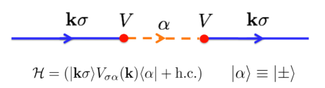
where the double and single arrows denote the localized moment and conduction electron respectively, as illustrated in Fig. 1 (a).
Each singlet has a ground-state energy per site and a singlet-triplet spin gap of magnitude . If we remove an electron from site , we break a Kondo singlet and create an unpaired spin with excited energy ,
| (6) |
while if we add an electron, the Kondo singlet is broken to create an electron quasiparticle, a composite involving an unpaired local moment and a doubly occupied conduction electron orbital
| (7) |
as illustrated in Fig 1(b). In this fashion, the strong coupling Kondo lattice with one electron per site forms an insulator with a charge gap of size and a spin gap of size .
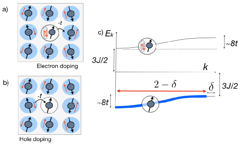
If we subsequently reintroduce the hopping between sites, then the quasiparticles become mobile, as illustrated in Fig. 1. Thus if we hole- or electron- dope the Kondo insulator by removing electrons, we end up with a narrow band of heavy quasiparticles or heavy electrons. In this way, Kondo insulators can be regarded as the parent compounds of heavy fermion metals.
1.4 Adiabatic picture
An alternative way to understand Kondo insulators in terms of adiabaticity was proposed by Richard Martin and Jim Allen [35]. The Kondo lattice Hamiltonian is a low energy limit of the Anderson lattice model,
| (8) |
where
| (9) |
describes the conduction electrons,
| (10) |
describes the atomic Hamiltonian of a localized f-state at site j in energy level and corresponding onsite Coulomb repulsive interaction , while
| (11) |
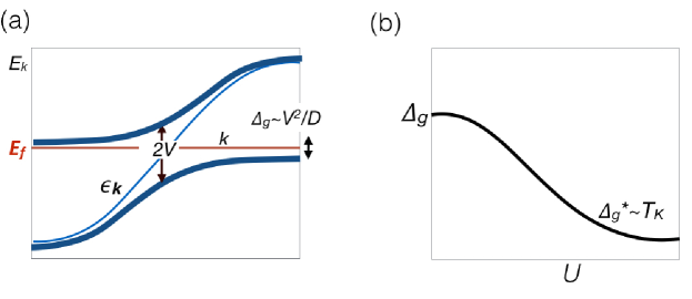
describes the hybridization between the localized state and the conduction electrons. At and half filling, this model describes a simple hybridized band-structure with a direct hybridization gap and an indirect gap , where is the half band-width, as first noted by Mott [31]. (See Fig. 2 (a)) By appealing to adiabaticity, Allen and Martin argued that as is increased, provided neutrality is maintained, the gap will simply renormalize downwards. At large , onsite charge fluctuations of the f-state can be eliminated via a canonical Schrieffer Wolff transformation [36] and in this limit, the model reduces to the Kondo lattice model with . Adiabaticity enables one to understand the Kondo insulator as simply the large cousin of the original hybridized band insulator, with a duality between weak and strong coupling in the two models:
| Large | Small | (12) | |||
| Small | Large | (13) |
The upshot of this discussion, is that the low energy physics of the Kondo insulator can be equivalently described by a renormalized Anderson lattice model, with renormalized parameters, , and determined by the Kondo temperature (See Fig. 2 (b)). Today there are various methods for calculating these renormalizations, including path integral [37, 38, 39], slave boson [40, 41, 42, 43, 44] Gutzwiller [45] and dynamical mean-field theory [46, 47, 48, 49] formulations of the Kondo and infinite Anderson models.
2 RISE OF TOPOLOGY
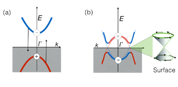
The concept of topological order has its roots in the pioneering work of Robert Laughlin, of David Thouless, Mahito Kohmoto, Peter Nightingale, Marcel den Nijs and of Duncan Haldane, on the integer quantum Hall effect or Quantum Hall Insulator [50, 51, 52]. From this work, the quantization of the Hall effect could be interpreted understood as a consequence of a topologically ordered ground-state wavefunction, in which the quantization of the Hall constant results from the integer-valued Chern number of the topology. Later work of Shuichi Murakami, Naoto Nagaosa and Shoucheng Zhang, of Charles Kane and Eugene Méle, and of Andrei Bernevig and Taylor Hughes, [53, 8, 9] led to the concept of the Spin Hall insulator: a two-dimensional topological insulator which is basically two time-reversed copies of the Quantum Hall Insulator.
In a series of remarkable papers, beginning around 2006, Joel Moore and Leon Balents, [10], Liang Fu, Charles Kane and Eugene Mélé, [12], and Rahul Roy [11] made the discovery that three-dimensional insulators can acquire a topological order through a spin-orbit driven band-inversion, leading to a new kind of insulator. From this new perspective, the presence of topological order is determined by a single Ising or Z2 index which is positive in conventional insulators (Z2=+1), but reverses sign in topological insulators (Z2=-1). Conventional insulators can be loosely considered as a miniature version of the physical vacuum. By contrast, topological insulators contain a internal twist to their wavefunction that prevents them from being adiabatically transformed into the vacuum of empty space, and this is why they innevitably develop surface states. We can imagine smearing out the surface of an insulator so that the the path from the insulator to the vacuum of empty space becomes an adiabatic deformation of the Hamiltonian. But if the vacua are topologically distinct, then the gap can not remain open along this path, or it would be possible to adiabatically deform the one into the other: as a result the insulating gap must collapse at the interface between two topologically distinct gapped states, to produce a gapless surface states. These states turn out to be Dirac surface states, with excitations whose spin is locked perpendicular to their momentum.
Conventional surface states are incredibly volatile and rarely survive as macroscopic conducting surfaces, since they are highly sensitive to disorder, which leads to Anderson localization and surface reconstruction, which eliminates the conducting states altogether. However, topologically protected surface states are robust against both Anderson localization and surface reconstruction, leading to the unusual situation where even cracks in the sample are conducting! The first two dimensional topological insulators were predicted in mercury cadmium-telluride (HgTe/CdTe) quantum wells by Andrei Bernevig, Taylor Hughes and Shou-Cheng Zhang [9] in 2006 and were discovered in 2007 by Lauren Mölencamp and collaborators [13]. The first experimentally realized three dimensional topological insulator was bismuth antimonide (Bi1-xSbx) [14], discovered by the groups of Robert Cava and Zahid Hasan in 2008.
In 2007, Liang Fu and Charles Kane showed that if an insulator has both time reversal and inversion symmetry [15], the index is uniquely determined by the the parities of the occupied Bloch states at the high symmetry points of the valence band
| (14) |
where is the the product of the parities of the occupied states at the high-symmetry points in the Brillouin zone. This beautiful index formula allows one to compute whether an insulator state is topological, merely by checking whether is negative.
Each time a band-crossing between an odd and even parity state occurs, the index changes sign (see Fig. 3), and provided , there will be protected Dirac surface states. For a cubic insulator, with high symmetry points at the , , and points, this formula reduces to . (The X and M point occur three times, but ). For example, if is the only negative parity, this means there have been three band crossings at the points, and in general this will give rise to up to three Dirac cone surface states.
2.1 Topology meets strong correlation
In 2010, Maxim Dzero, Kai Sun, Victor Galitski and Piers Coleman [16] proposed that Kondo insulators can form strongly interacting versions of the topological insulator. The key points motivating this idea were that:
-
•
The spin orbit coupling of f-electrons in a Kondo insulator, of the order of eV, is much larger than the characteristic gap of a Kondo insulator, making these essentially infinite spin orbit coupled systems, ideal candidates for spin-orbit driven topological order.
-
•
f-states are odd-parity, whereas the predominantly d-band conduction bands that hybridize with them are even parity, so that each time there is a band-crossing between the two, the index changes sign, leading to a topological insulator.
The TKI proposal provides an appealing potential resolution of a long-standing mystery in the Kondo insulator SmB6, which for more than thirty years, had been known to exhibit a low temperature resistivity plateau [54, 55] (see Fig. 7), which could be naturally understood as a consequence of topologically protected surface states [16, 56]. In 2012, teams at the University of Michigan [17] and the University of California, Irvine [18], confirmed the existence of robust surface states in SmB6. Most recently 2014 [57] Xu et al. have detected the spin-polarized structure of the surface states in these materials that tentatively confirm their topological character (see discussion in section 4.2).
3 THEORETICAL MODEL OF TOPOLOGICAL KONDO INSULATORS
In this Section we review the models, which have been recently proposed to describe various topologically nontrivial electronic states in Kondo insulators. We begin by introducing a general model for the topological Kondo insulators and discussing the conjecture of adiabatic connectivity between band insulators and Kondo insulators. This discussion is then followed by the review of the tight-binding models specific to Samarium hexaboride.
3.1 General discussion
The Anderson lattice model (ALM), consisting of a set of localized -electron states, hybridized with conduction electrons, provides a basic description of the physics of -electron materials. The ALM Hamiltonian has the form
| (15) |
Here describes the -electron system and can be written as follows:
| (16) |
where are the hopping amplitudes for the -electrons between neighboring sites on the lattice, is a fermionic annihilation operator and is the strength of the Coulomb repulsion between the -electrons on the same site. The interactions between the conduction electrons are ignored.
In the simplest models of Kondo insulators the -electrons are considered as dispersionless, localized states, . However, in the context of topological Kondo insulators, where the hybridization contains nodes, a more general model with nonzero off-diagonal elements of is required (see our discussion below). Inside a crystal, the intrinsic degeneracy of the -states, is lifted by the spin-orbit coupling and the crystalline fields, and the subscript in (15) labels the components of the low-lying spin-orbit split -multiplet.
The second term in (15) accounts for a band of non-interacting conduction electrons:
| (17) |
where labels the projection of conduction electron’s spin, accounts for the degeneracy of the corresponding conduction orbitals due to non-zero angular momentum and is the hopping amplitude. Note that the intersite hopping terms in (16) and in (17) are not necessarily limited to the nearest neighbor sites. Lastly, the hybridization term in the Hamiltonian (15) is
| (18) |
with being the hybridization matrix diagonal in momentum space:
| (19) |
The important point, is that all the spin-orbit coupling, all the topology is hidden inside the hybridization matrix. The specific form of the hybridization matrix will depend on the multiplet structure of the f-electrons as well as on the angular momentum of the conduction electrons. However, typically the conduction electrons are composed of even parity d-states, hybridizing with the -electrons, which have odd parity [5]. It follows that at the high symmetry points in the Brillouin zone , parity is a good quantum number and as a result, the odd-parity f-states and the even parity d- states can not mix, so that . More generally, since the Hamiltonian must be even under the parity operation, any hybridization matrix that mixes even and odd parity electron states must itself be an odd-parity function of momentum
| (20) |
i.e. the elements of the hybridization matrix are odd functions of momentum. We can see this more detail by noting that at a high symmetry point, the effect of reversing is the same as shifting it by a reciprocal lattice vector , , and since the hybridization is periodic in , i.e , it follows that . Comparing this with (20 ), it follows that as expected. The presence of nodes in the hybridization at the high symmetry points is central to a description of topological Kondo insulators.
3.1.1 Non-interacting limit and adiabatic continuity
Let us consider the simplest case when the interaction between the -electrons is zero, . In this case, the model Hamiltonian (15) describes two hybridized bands of non-interacting electrons as illustrated in Figure 2 (a), with a direct gap of order and an indirect gap of the order of (where is the typical size of the hybridization and is the conduction electron bandwidth). The insulating ground state in this model corresponds to the case of half-filling, so that the lower bands become fully occupied. For example, in the simplest case of a single-Kramers-degenerate conduction electron and -orbital Kramers doublet, an insulating state is realized when there is exactly one conduction electron and one -electron per site.
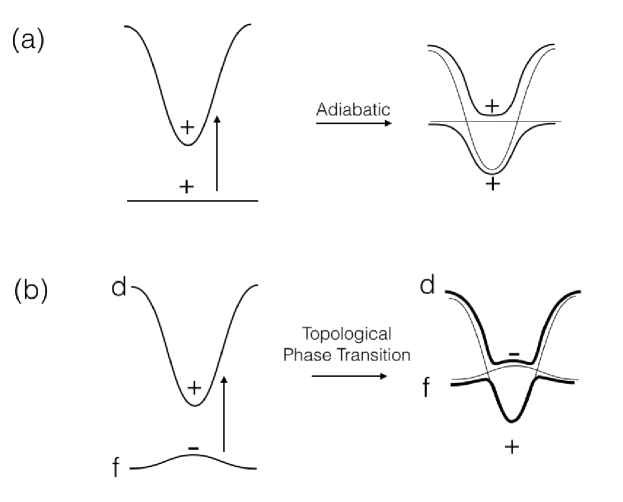
Does the system remain insulating if we adiabatically switch on the interaction ? In their pioneering work Martin and Allen [35, 58, 59] argued using Luttinger’s theorem, that as long as the band remained half-filled, there would be no reason for the gap to close (See Fig. 4 a). Numerical studies within the self-consistent fluctuation exchange approximation have largely confirmed this conjecture at least for moderate values of . [5, 60] Theoretical schemes based on the variational wave-functions [32] also seem to suggest the validity of the Martin-Allen conjecture even for .
However, topology complicates adiabaticity arguments [16, 56]: : in particular, as we saw in the last section, when the parities of the conduction and f-bands are opposite, the hybridization vanishes high symmetry points, and this opens up the possibility that interactions will induce band-crossing, changing the topology of the ground-state. For example, let us assume that in the non-interacting limit, the ALM Hamiltonian is topologically trivial, with a completely filled band of f-states (See Fig. 4 b). For a system with time-reversal and inversion symmetry, the topological invariant is determined by the parity operator eigenvalues [15]. For the ALM and taking into account (20) it is simply given by
| (21) |
where is a momentum at one of the eight high-symmetry points of the 3D Brillouin zone and is the dispersion of the conduction and the -electrons correspondingly. As we switch the interaction adiabatically the conduction d-band and f-bands will renormalize, with the f-level moving upwards relative to the conduction bands due to their stronger Coulomb interaction, . If as a result of this process, the f- and d- bands cross at an odd number of points, then a topological phase transition will take place into a topological insulator (see Fig. 4 b). Since two topologically distinct states cannot be adiabatically connected without closing the gap, this phase transition must be accompanied by a momentary closing of the gap at a particular critical values of . In this way, adiabaticity can break-down. Recent studies by Werner and Assaad [61] of the periodic ALM on the two-dimensional square lattice have found that increasing the strength of the Hubbard interaction leads to the series of transitions between normal insulator (small ) into a strong topological insulator with the band inversion at the point and then into another strong topological insulator, in which bulk bands invert at the point of the two-dimensional Brillouin zone.
From this discussion, it becomes clear that in order that the Allen-Martin idea of adiabaticity to topological Kondo insulators, then the interaction and the strength of the spin-orbit interaction in the Hamiltonian must be tuned so that no band crossing takes place. Since interactions have the effect of narrowing the bands, in practice, this will mean starting with a Hamiltonian with Hamiltonian with a greatly enhanced value of the spin-orbit coupling.
3.1.2 Model for topological Kondo insulators with Kramers doublets
The simplest model for a topological Kondo insulator contains a single -band of conduction electrons hybridized with a single Kramers f-doublet, with nearest neigbor hopping and hybridization, Fig. 5. The resulting non-interacting Hamiltonian has the form:
| (22) |
where
| (23) |
describe the dispersion of the conduction and f-band, while
| (24) |
is a vector in spin space, which approximates to in the vicinty of the point. Notice how all the spin orbit coupling effects are held by the hybridization. In the special case where , this Hamiltonian is a simple lattice generalization of the mean-field Hamiltonian for the gapped topological superfluid phase of Helium, He-3B[62, 63]. The non-interacting band dispersion described by this Hamiltonian is simply
| (25) |
This model has been employed to great success in a number of recent publications [64, 65, 66, 67].
The low energy properties of the interacting model with the Hamiltonian
| (26) |
can be analyzed by either employing the conjecture that the effect of the local correlations between the -electrons leads to the renormalization of the hybridization amplitude and the shift of the -energy level (see e.g. [16, 56] and references therein). Alternatively, one can set and project out the doubly occupied -states by introducing the slave-boson operators [5, 68]. The slave-boson mean-field theory corresponds to replacing operators by -numbers which are computed self-consistently. The result of the above mentioned procedure is a renormalization of the unperturbed bands (22):
| (27) |
where is an average -level occupation number. Lastly, the position of the bare -electron level shifts from below the chemical potential for the conduction electrons to energies above it. Subsequent analysis of the topological invariant (21) yields the odd number of band inversions for intermediate values of - mixed-valence regime - and even number of band inversions for - local moment regime. [16, 56] The latter corresponds to the so called “weak topological insulator” with the topological invariant given by
| (28) |
where denotes a plane perpendicular to one of the main crystalline axes.
An appearance of the weak topological insulating state for raises a general question whether it would be in principle possible to stabilize the strong topological insulating state () in the local moment regime. To address this issue Dzero [68] has generalized conduction and -electron Kramers doublets to components and used the symplectic SP() () representation for the electronic operators to properly account for time-reversal symmetry of the conduction and -electron states. In agreement with the previous results [16, 56, 69] he found that for and there appears two (weak and strong) topologically non-trivial states depending on the relative position between the renormalized -level and the chemical potential of the conduction band. Interestengly, for the large value of there is only strong topological insulating state. Thus, the higher degeneracy of the -electron multiplet favors the strong topological state. This result has been later confirmed by considering the tight-binding model for Samarium hexaboride (SmB6) with the fourfold degenerate -orbital multiplet. [70]
3.2 Tight-binding models for Samarium hexaboride
Samarium hexaboride has recently emerged as a prototypical candidate for the first experimental realization of strongly correlated topological insulator. Perhaps one of the most intriguing problems concerns the role the electronic correlations play in determining the parameters of the helical surface states such as the effective mass of the surface electrons and characteristic length scale on which surface states penetrate into the bulk. Thus, the formulation of the realistic and yet tractable tight-binding model presents a first important step towards a better understanding of the physical properties of SmB6. Below we review the recent theoretical models which have been put forward to describe the formation of the topological surface states in this material.
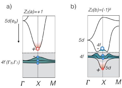
The key insight for building realistic tight-binding model for SmB6 came from a detailed first-principle calculations of Yanase and Horima [71] and of Antonov et al. [72] Their calculations show that the Samarium orbitals hybridize exclusively with Samarium -orbitals [71, 72]. The crystal field splitting of the -multiplets leads to a low-lying doublet at the point. Away from the point, the orbitals split into two Kramers doublets, the lower one dipping down at the point, where it dives through the the bands. Hybridization between the two bands forces 4f states from the valence to the conduction band, forming heavy 4f electron band pockets at the X points. Once the d-band crosses through the f-band at the three points, so long as there are no other crossings, the resulting non-interacting band-structure is innevitably topological, independently of the details of the f-multiplets (See Fig. 6).
Infact, in the cubic environment, the six 4f orbitals of the Samarium split into a doublet and a quartet. LDA studies [71, 72] suggest that the physics of the orbitals is governed by valence fluctuations involving electrons of the quartet and the conduction states, . The () quartet consists of the following combination of orbitals: . This then leads to a simple physical picture in which the quartet of -states hybridizes with an quartet of -states to form a Kondo insulator.
In 2011, Takimoto [73] introduced a tight-binding model for SmB6 in which the hopping amplitudes in the Hamiltonian (15) are non-zero for nearest- and next-nearest-neighbors, while hybridization involves the nearest-neighbor overlap integrals only. The values of the hopping amplitudes were adjusted to fit the LDA band structure results, while the effect of interactions between the -electrons is modelled as a renormalization of the bare -energy level and the hybridization. In Takimoto’s model, a singlet -like orbital inverts with an -like orbital at the X point of the bulk Brillouin zone, while the remaining two bands remain inert. This band inversion at the X points implies the existence of three Dirac cones on the surface: one at the surface point and two at the points. Interestingly, the corresponding Fermi velocities for the electrons at the point are the same, while the Fermi velocities at the are strongly anisotropic. [73]
Alexandrov and collaborators [70] have considered a simpler tight-binding model only nearest neighbor hopping amplitudes only, showing that the LDA band structure results are recovered by using the appropriate Slater-Koster[74] ratio of the overlap integrals between and orbitals. By setting and employing the slave-boson mean-field theory, it was shown that strong topological insulator state extends all to way to the local moment regime, . It was also emphasized that quite generally, cubic topological insulator can only be realized when bands invert at the or points, since at the and points the - and -bands are doubly degenerate and therefore remain topologically inert - the parity eigenvalues at these points are always positive.
Legner and collaborators have considered an even simpler model for cubic topological insulators. [64], involving one Kramers degenerate - and -orbitals. These authors have focused on the general topological properties which are possible in the presence of the cubic symmetry. The hopping terms in the tight-binding model [64] involve amplitudes between nearest-, next-nearest- and next-next-nearest neighbors. As a result, for various choices of the hopping amplitudes various topologically non-trivial states including the one where - and -bands invert at the X points. Legner et al. have also derived the surface state dispersion and found that the Fermi velocity for the electrons is
| (29) |
This result implies that the effective mass of the surface electrons is quite heavy since the hybridization amplitude is small compared to other relevant energy scale, while the expression under the square root is of the order .
4 RECENT EXPERIMENTAL PROGRESS ON SmB
Kondo insulators, in particular SmB are prototypical strongly-correlated mateirals featuring f-electron physics and some highly unusual electronic properties. As discussed earlier in this review, the theory of Kondo insulators has predicted in some KI materials the existence of a topologically nontrivial surface state with an odd number of Dirac surface bands. In the past two years tremendous experimental progress has been made on SmB seeking to identify the existence of the metallic surface state, to test the topological properties of the surface state and to search for correlation physics. Below we review some of these experimental works. We note that despite the rapid progress of the field, questions remain about the exact nature of the surface state, the consequence of multiple surface bands, and unusual surface properties due to interaction within the surface state and between the surface and bulk Kondo lattice. The surface state of SmB (and possibly other TKI candidates) a good experimental platform to explore unusual quantum phases involving strong electron correlations, heavy fermion physics and topological order.
4.1 Transport evidence for the metallic surface state
SmB (Fig. 7a) is a classic Kondo insulator [3]. As discussed above, the strong interaction within a localized periodic dense array of localized f-magnetic-moments leads to a re-organization of the electronic structure at low temperatures [3] resulting in an energy gap driven by hybridization between conduction electrons and the highly renormalized f-electrons. When the Fermi level lies within the Kondo energy gap, an insulator is formed. As a result, SmB behaves as a correlated metal at high temperatures [1], and becomes insulating below 40 K with the opening of Kondo gap [3], yielding an activated diverging resistance at low temperatures. This is illustrated in Fig. 7b. However, at even lower temperatures below 4 K, a peculiar resistance saturation was found in the original experiments of Menth et al. [1] and Allen et al. [54] (see Fig. 7c). This additional metallic conduction channel was initially suspected to originate from bulk impurity states [1], but the improvement of the sample quality does not seem to reduce the low temperature saturation behavior [1, 54, 75, 76, 18]. The theory of topological Kondo insulator by Dzero et al. [16] predicted the existence of a topologically protected metallic surface state (TSS) within this Kondo gap, naturally accounting for the resistance saturation. Experiments soon followed to verify whether the low temperature conduction does indeed occur on the surface.

In 2012, signs of a low-temperature surface state were obtained while investigating the capacitive self-oscillation effect in SmB single crystals. Recording the Lissajous plots of current-induced voltage oscillations, Kim et al., [77] detected an anomalous capacitance component (F) in mm-sized SmB crystals below 4K. This was almost exactly the onset temperature of the saturation resistance, hinting at a common origin. The response of the SmB crystal closely resembles that of a 2 resistor in parallel with a 2F capacitor, as shown in Fig. 8a. Since a RC circuit is equivalent electronically to an insulating material encapsulated with a conducting surface in a bulk material, the surface conduction picture was a natural explanation for the anomalous capacitance. However, despite this strong evidence for surface conduction, alternative scenarios could not be ruled out (e.g. having many insulating grains embedded in a conducting bulk could also lead to an equivalent RC circuit, as depicted in the inset in Fig. 8a). This motivated further transport studies.
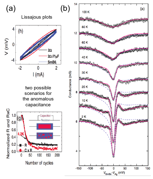
One way to prove that SmB is truly insulating in its bulk is to show that the bulk density of states (DOS) remains unchanged below the resistance saturation temperature. This can be done by measuring the resistance of a very fine contact to the sample: a technique called Point-Contact Spectroslcopy (PCS). If the low temperature residual conduction arises from bulk impurity state or the above-hypothesized metal-insulator mixture instead of a metallic surface, the bulk electronic state would necessarily change when the coherent conduction channel develops at low temperatures. Zhang et al. [78] performed PCS on SmB using Ag particle point contacts. They recorded the point-contact conductance as functions of both Ag-SmB voltage difference and temperature (Fig. 8b). The former conductance-voltage relation, or conductance spectra, give valuable information regarding the bulk electronic structure at a given temperature. Zhang et al. [78] observed the onset of a zero-bias conductance dip below 100K, signaling the opening of the Kondo gap due to electron correlations. Perhaps the most striking finding of the experiment is that the conductance spectra remained unchanged while the temperature was lowered from 10 K to 2K, where the sample resistance saturation occurred. This proves directly that during the resistance saturation, the bulk of SmB remains insulating with an almost constant Kondo gap. The most natural explanation of this phenomenon is to assign the low-temperature metallic conduction to the surface.
The low-temperature surface conduction could also be demonstrated somewhat more directly by noticing that the bulk and surface contributions to conduction vary differently as one changes the size and shape of the sample. Wolgast et al. [17] designed and fabricated a thin-plate-shaped SmB crystal (Fig. 9a) in order to enhance the difference between bulk and surface contributions. The electric current leads were placed on the top and bottom sides of the sample, which was sandwiched between two insulating silicon pieces. For the bulk conduction in this SmB plate, the current can zip through the middle thin part of the crystal; while the surface current has to travel along the surface around the corners of the sample. Therefore, voltage leads, placed at various locations on the sample, could register these two vastly different current paths. In their experiments [17] three voltages (Fig. 9a) are measured as a function of temperature. After comparison between theoretical simulations and experimental results, it was found that surface conduction indeed dominated at low temperatures, while bulk contribution dominated at high temperatures [17].
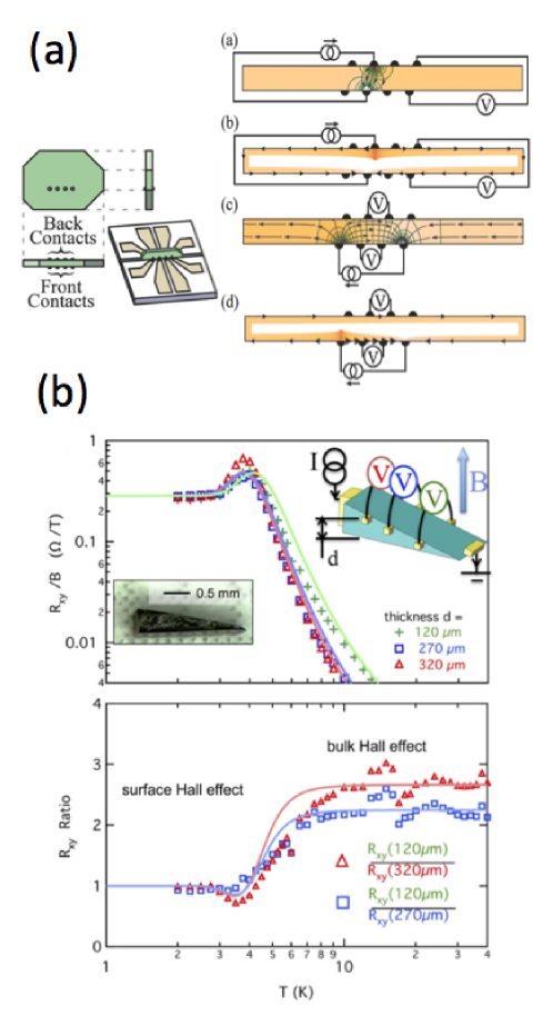
Another transport quantity that would differ sharply between surface and bulk conduction mechanisms is the Hall effect. In a perpendicular magnetic field, the transverse or Hall voltage is inversely proportional to the thickness of the Hall bar in the case of the usual bulk conduction. However, if surface conduction dominates, the thickness of the Hall bar is irrelevant and the Hall voltage would be thickness-independent. Therefore the thickness-dependence of the Hall effect should directly indicate whether bulk or surface conduction dominates. A technical difficulty associated with such an experiment is the innevitable variability in crystal thicknesses.
This problem was solved in an experiment by Kim and Thomas et al. [18] who measured Hall voltages at different thicknesses, within the same crystal using an SmB Hall bar shaped into a thin and long wedge (Fig. 9b). In smooth, well-polished SmB wedges, they found that the high temperature Hall resistance R = V/I was inversely proportional to the thickness, consistent with bulk transport [18] . The temperature dependence (Fig. 9b) of R follows an activated behavior with a transport activation gap of 38K, confirming the insulating nature of the bulk. However, at temperatures below 4 K, the Hall resistance R becomes thickness-independent, proving the domination of surface conduction. At these temperatures, the R is also temperature independent, consistent with the metallic nature of the surface conduction. Without a magnetic field, the qualitative evidence for low temperature surface conduction was also obtained in Ref. [18] by comparing the local and non-local voltages on thin-plate samples, as was used in non-local voltage measurements [79] in quantum Hall effect systems to identify the then-debated edge state conduction. This measurement is conceptually equivalent to the thin-plate measurement described above [17], both taking advantage of the vastly different paths of surface and bulk conductions. Several samples were used for both Hall and non-local measurements, including purposely scrapped samples. And the surface dominated conduction was found to hold independent of the crystal surface direction or surface quality, which is consistent with a topologically protected surface state that can only be destroyed by broken-time-reversal, e.g. magnetic, perturbations.
Perhaps an even more vivid demonstration of the low temperature surface conduction is to show that the longitudinal resistance doesn’t depend on the thickness of thin samples. In such an experiment, special care needs to be taken to preserve the surface quality before and after the thinning process. Nevertheless positive results have been demonstrated by several groups now [77, 17, 78, 80].
4.2 ARPES studies of the surface state
The electronic structure of the surface state can be probed directly by angle-resolved photoemission spectroscopy (ARPES). An observation of odd number of Dirac surface bands would be a direct confirmation of the topological nature of the surface state. In addition, spin-resolved ARPES can in principle investigate the spin structure of the surface state. This has led to a flurry of recent ARPES studies of SmB . Because of the limited energy resolution of ARPES relative to the small Kondo gap of SmB , the detailed spin structure of the surface states is currently still contraversial[57, 81]. Important insights regarding the energetics of the surface state have been nevertheless been obtained by several recent ARPES studies. Before we review these experimental results, it would be helpful to first take a look at the predicted SmB energy spectrum for a topological Kondo insulator obtained by Lu et al. [82]. Another calculation has been carried out by Alexandrov et al. [70]. One calculated energy spectrum [82] is shown in Fig. 10a for the first Brillouin zone (BZ) in (001) surface, where high-symmetry points are labeled as , X, and M. The blue lines are bulk energy levels with a Kondo gap at the Fermi level. And the red lines are surface states, showing three Direct cones at , and the two X points.
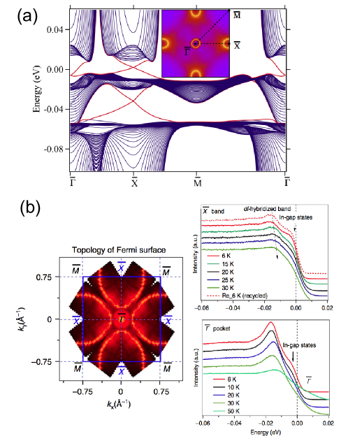
The ARPES results of Neupane et al. [83] are replotted in Fig. 10b for direct comparison. The topology of the measured Fermi surface at 6 K agrees well with the topological Kondo insulator calculation (Fig. 10a). As predicted, three low-lying metallic states near the Fermi energy exist at the , and the two X points. The two X pockets are quite large, suggesting that the Fermi energy is far away from the (possible) Dirac points at X points. Two other important results are obtained by Neupane et al. [83] from the temperature evolution of the ARPES spectral intensity (Fig. 10b). The first is that the in-gap metallic state only emerges at temperatures below 15 K for both and X pockets, suggesting the nontrivial origin of the metallic state. The second finding is that the metallic in-gap state does not disappear after a 6 to 50 K thermal recycling, which demonstrates that the in-gap states are robust and protected against thermal recycling.
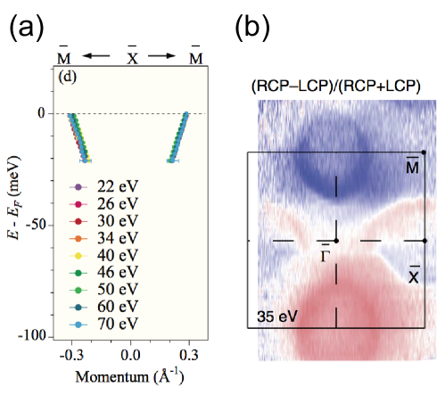
Two additional ARPES results by Xu et al. [84] and Jiang et al. [85] were reported at the same time which are consistent with the topological Kondo insulator scenario for SmB6. In particular in Ref. [84], Xu et al. extracted the energy dispersions of the band (X pocket) (Fig. 11a). The linear dispersions demonstrate the two-dimensional nature of the pocket. Unfortunately the Dirac points could not be observed clearly in this study. For the band, Xu et al. found that the intensity diminishes suddenly at 20 meV below Fermi level, corresponding to the hybridization gap edge between f and d electrons. They argue that this may prohibit observing the Dirac point formed by the bands crossing each other. In [85] Jiang et al. performed circular dichorism (CD) ARPES measurements. CD ARPES may shed some light on the spin structure of the metallic state. Jiang et al. calculated the differential map of the photoemission intensities with right-circularly-polarized (RCP) and left-circularly-polarized (LCP) lights as repotted in Fig. 11b. The anti-symmetric pattern with respect to the -X line resembles that of a topological surface state. However, it is not yet sufficient to make conclusive statements about the surface spin texture or Berry’s phase [83] due to several complexities related to CD ARPES.
Parallel ARPES studies on SmB were carried out by Zhu et al. [86] and Denlinger et al. [87] respectively. In Ref. [86], Zhu et al. propose an alternative explanation for the conducting surface state, suggesting that it originates from boron dangling bonds on the (001) crystal surface, i.e. that it is a non-topological polar surface. In [87] Denlinger et al. found high ARPES intensity at the H points, where the momentum-location of the H-point along the -M direction coincided with the polar metallic surface state claimed by Zhu et al. [86]. However, Denlinger et al. [87], found that the H-point is gapped at low T temperature, suggesting that the polar surface state found by Zhu et al. [86] is in fact insulating and hence unrelated to the metallic surface state. Due to the limited resolution, it is somewhat hard to judge which scenario is correct at the moment. However, the (001) polar metallic surface picture by Zhu et al. [86] seems to contradict available transport experiments that showed the existence of surface metallic conduction on both (001) and (011) surfaces. The latter surface is not polar and therefore can not host a polar metallic surface state.
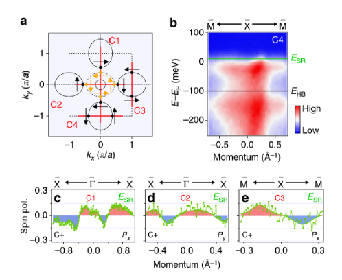
Finally we mention the current status of spin-polarized ARPES measurements. In weakly interacting topological insulators, the classic test for topological Dirac states, is to directly observe their spin texture using spin-resolved ARPES measurements[88]. However, in SmB6, the narrowness of the bulk insulating gap makes this a highly challenging measurement, the results of which are still contraversial. The first spin-polarized ARPES measurements have been carried out on SmB6 were carried out at the Swiss Light Source[57]. These measurements show of spin-momentum locked states on the 100 surfaces in the vicinity of the points in the surface Brillouin zone (see Fig. 12), supporting the presence of topological Dirac states. However, spin-polarized ARPES measurements carried out at the Helmholtz-Zentrum, Berlin[81] have led this group to question the topological interpretation. In particular, their measurements around the points appears to support the presence of Rashba-split, conventional surface states of a trivial insulator. The resolution of this experimental controversy awaits improved resolution and further measurements.
4.3 STM studies of the surface state
Scanning Tunneling Microscopy (STM), is another useful surface probe with the potential to reveal the properties of the surface states with atomic spatial resolution. Spectroscopic measurement of the tunneling conductance as a function of bias voltage, or Scanning Tunneling Spectroscopy (STM) further reveals the local density of states near the Fermi energy. Therefore a temperature-dependent STS study would tell quite a lot about the energetics of bulk and surface state, complementary to ARPES measurements.
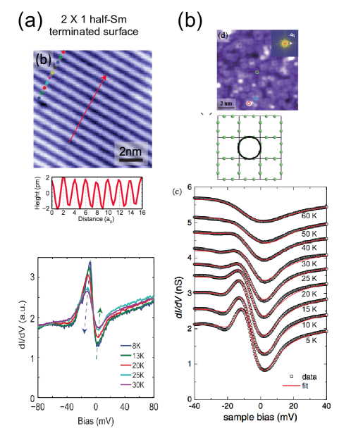
STM and STS study on the (001) surface SmB by Yee et al. [89] revealed that the surface of SmB is quite complex and far from an ideal. Their STS morphology image of the normal (001) surfaces shows that much of the surface reconstructs to a structure in which half the surface is samarium-terminated (See: Fig. 13a). Other regions of the surface appear amorphous and only small regions involve a pristine termination. It is unclear at this stage if the reconstruction is due to the particular cleavage method or whether it is intrinsic to SmB . Nevertheless, this STM study suggests that the ARPES studies, which have optical spot sizes of hundreds of microns could have picked up a mixture of spectra from a variety of different surface morphologies. This may explain in part the limited resolution of SmB ARPES measurements.
In the STM study by Yee et al. [89] a common STS spectra feature was observed for both and regions: a minimum of dI/dV at the Fermi level and a gap (dI/dV peak) slightly below this minimum in energy. Fig. 13a shows the STS spectra for the case of region, where the peak is centered at - 8 meV and becomes smaller at higher temperatures. Extrapolating to high temperature, Yee et al. argued that the peak (gap) would vanish at 40K, suggesting its hybridization nature. They also observed residual spectral weight spanning the hybridization gap down to the lowest temperatures, which is consistent with a topological surface state. Qualitatively similar findings were observed for the surface region, although the energy is shifted by tens of eV. This testifies the robustness of the hybridization gap. In the other STM work [90] by Ruan et al., four types of surface morphology were found, highlighting again the complexity of the SmB surface. The STM image for the “Donut” D2 phase is shown in Fig. 13b with a cartoon illustrating the “Donut” structure. The temperature dependence of the STS spectra (Fig. 13b) is qualitatively similar to those found by Yee et al. The data revealed the emergence of a resonance peak below 40K, signaling the opening of the Kondo gap. Summarizing the body of all STM works, the large zero bias conductance that persists to the lowest temperature may come from the topological surface state. However a smoking gun STM evidence for TKI is still lacking: the quasiparticle interference patterns showing surface state with helical spin texture.
4.4 Is the surface state topological?
The experiments reviewed up to this point, provide strong evidence for the existence of the metallic surface state that emerges from an insulating bulk state at low temperatures. The metallic surface state could be conveniently probed by transport methods due to the insulating nature of the bulk. Although the low temperature emergence of the surface state [83] and the antisymmetric ARPES pattern with opposite chirality of light [85] seem to be consistent with a topological surface state, more direct evidence is still needed to tell whether the surface state is really topological. In an ideal world, energy- and spin-resolved ARPES conducted at low temperatures below the resistance saturation would confirm whether the spin texture of the surface state has a Berry phase. However, the required high energy resolution (few meV) is beyond the current capability of both synchrotron ARPES (40 meV) and laser ARPES (10 meV). Other difficulties derive from the limited low temperature range and spin resolution with spin-resolved ARPES techniques. It is noted that other TKI candidates may possess larger Kondo gaps, making them to be within the resolution of current spin-resolved ARPES capabilities. As mentioned above a smoking gun STM evidence for the topologic surface state would be the quasiparticle interference patterns showing surface state with helical spin texture. This might be within the capability of current STM techniques, if a better surface without reconstruction could be prepared for STM studies.
Since the bulk of SmB is insulating at low temperatures, it is possible to test the topological properties of the surface state, giving partial evidence for the topological surface state. A topological surface state has three aspects of topological protection. First, their fundamental Z2 topology preserves a gapless surface state unless time reversal symmetry (TRS) is broken. Second, helical spin polarization prevents momentum backscattering from to k by non-magnetic impurities. Finally, the Berry phase protects the surface state from weak localization through time reversed paths. These collectively provide a robust surface state with TRS conservation. Therefore for a topological surface state, it could only be made insulating by broken TRS such as those created by magnetic perturbations. In addition, such a surface state would become less conductive when a small magnetic field is applied, destroying the negative interference between time-reversed carrier paths. This is called the weak-antilocalization (WAL) effect [94]. These two experimental tests have been carried out by Kim et al. [91] and Thomas et al. [93] and both have yielded positive results in agreement with a topological surface state.
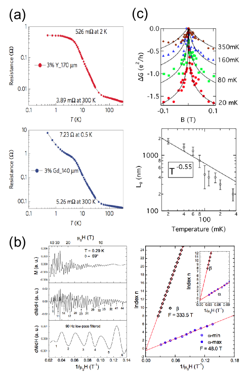
Kim et al. [91] made a comparison study between SmB crystals with magnetic (Gd) impurity doping and non-magnetic (Y or Yb) impurity dopings. In those thin-plate shaped samples, surface vs bulk conduction could be distinguished by performing thickness dependence measurements: when surface conduction dominates, the resistance ratio should be irrelevant to thickness. Kim et al. found that Yb and Y doped SmB exhibit bulk conduction at high temperature and change to surface conduction at low temperatures, similar to pure SmB . In contrast, the resistance of Gd doped SmB remains inversely proportional to sample thickness for all temperatures, indicating bulk-dominated conduction even at low temperature. A perhaps more direct illustration of the contrasting impact from magnetic and non-magnetic dopings is plotted in Fig. 13a. Below 4 K, the resistance of the Y doped sample saturates just like in pure SmB , while the Gd doped sample shows insulating behavior. Only the broken TRS magnetic doping destroys the metallic surface state. It is noted that in this study, the amount (3 percent) of Gd doping is sufficiently small to not introduce order magnetic states, as evidenced from the magnetic measurements [91].
Weak antilocalization (WAL) [94] is expected in a topological surface state due to an unusual Berry phase of [7, 6], which causes destructive interference between time-reversed electron paths and lowers the sample resistance. This effect is destroyed by a time-reversal-symmetry-breaking magnetic field, giving rise to magneto-resistance dip around zero field. Unfortunately, WAL alone can not provide conclusive evidence of a topological surface state because strong spin-orbit coupling can also produce a WAL effect. Indeed Thomas et al. observed clear WAL effect in SmB samples at low temperatures [93]. As shown in Fig. 13c, the WAL manifests itself as a conductance peak at zero field, with the height of the peak decreases at higher temperatures. The shape of the WAL feature fits well to the Hikami-Larkin-Nagaoka (HLN) equation [95]. The temperature dependence of the coherence length could be extracted using the fittings, suggesting that below 80 mK, electron-electron interaction dominates the scattering of transport current. The WAL effect has also been detected by Nakajima et al. [96].
The topological aspect of the surface state could also be probed by quantum oscillations: the periodic variation of physical properties of the sample as the Landau levels pass through the Fermi level in a changing magnetic field. For a topological surface state with odd number of Dirac points, the Berry’s phase would be instead of the usual value of 0. As a result, the Landau level index would be half-integer at the large field limit. Using a sensitive torque magnetometry setup, Li et al. [92] have recently reported the detection of de Haas van Alphen oscillations (dHvA) in the magnetization of SmB crystals. Fig. 13b shows two types of dHvA oscillations in that sample, identified as the (001) and (011) surfaces respectively. The Landau level index of both oscillations extrapolate to -1/2 at the high field limit, suggesting a non-trial Berry phase of in both energy bands. Their experiment finds that the frequencies of the observed oscillations only depend on the perpendicular component of the field, as expected for a surface state. One of the intriguing aspects of the measurements, is that the quasiparticle effective mass obtained the temperature dependence of the signal is about 0.1me. This small mass is unexpected on the basis of the “Heavy Fermion” nature of SmB . More experimental and theoretical investigations are needed to understand this discrepancy.
5 OPEN QUESTIONS
Topological Kondo insulators represent a collision of three areas of research: topological matter, strongly correlated systems and surface science, and experts from each of these fields find themselves outside their comfort zone. It is against this backdrop that SmB as a candidate TKI poses a immense new theoretical, experimental, and materials science challenges.
The physics of Kondo insulator SmB originates from a periodic dense lattice (Kondo lattice) [3] of localized magnetic moments, and is quite different from the Kondo effect [97] of isolated magnetic moments. Moreover, while it may be adiabatically connected to a topological band insulator, the system also lies at the brink of magnetism. Indeed, high pressure experiments show that at pressures of about 9GPa, the hybridization gap of SmB6 closes, leading to the development of magnetic order[98, 99]. This raises many interesting questions and possibilities, for instance:
-
•
What is the effect of the surface on the Kondo effect?
-
•
Could the bulk and its excitations be different in any way from a conventional insulator?
-
•
Will magnetism emerge on the surface, and if so, what kinds of highly correlated and competing order are realized near the point of instability?
-
•
Finally, what is the effect of disorder, such as vacancies or “Kondo holes” at the Samarium sites?
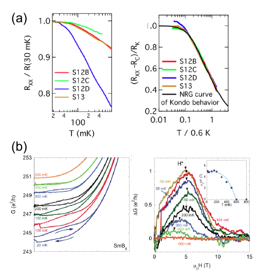
In a study by Thomas et al. [93] who followed the saturated resistivity of SmB to mK temperatures, the resistivity was found to exhibit a temperature dependence (Fig. 15a) before the final saturation below 40 mK. The size of the behavior is both sample-dependent and inconsistent with the WAL effect alone even with the correction of electron correlation. However, the temperature dependence can be perfectly explained by assuming the Kondo effect in the surface state driven by by Kondo holes, with a universal Kondo temperature of 0.6 K. In fact, the data from several samples could be scaled into a single numerical renormalization group calculation of Kondo effect behavior assuming a single Kondo temperature (Fig. 15a).
Nakajima et al. reported hysteresis in magneto-resistance [96] in a SmB sample, as shown in Fig. 15b. The hysteresis may originate from ferromagnetic state on the surface, which they hypothesize to arise due to Kondo holes. The edge state between magnetic domains of opposite chirality could in principle yield quantized (Hall) conductance. Nakajima et al. observed that the hysteretic part of the longitudinal conductance lies within the range of the quantum conductance (Fig. 15b), hinting the aforementioned mechanism.
It is clear from these examples, that the effects of interactions on topological surface states pose a major challenge. There have been a number of recent theoretical publications that have started to explore these issues [100, 101, 65, 102]. Bitan Roy and collaborators[101] have emphasized an itinerant description of the interacting surface Dirac cones and in[102] predict a proclivity towards excitonic and nematic instabilities. The papers [100, 65] discuss the physics in terms of a surface Kondo lattice involving local moments interacting with chiral surface states. Alshuler and Aleiner have considered a simplified one-dimensional surface state, and show that interactions with the local moments will localize surface states. Alexandrov, Erten and Coleman[65] have proposed a similar two dimensional model and propose that the surfaces of topological Kondo insulators may develop quantum critical ground-states.
One of the outstanding puzzles concerns the very high group velocities of the surface states of SmB6 measured in experiment. Both quantum oscillation[92] and ARPES studies[84, 85, 83], show the surface quasiparticles are light. ARPES measurements indicate surface quasiparticles with Fermi velocities ranging from 220[85] to 300 ∼30-50meVÅ_6
DISCLOSURE STATEMENT
The authors are not aware of any affiliations, memberships, funding, or financial holdings that might be perceived as affecting the objectivity of this review.
ACKNOWLEDGMENTS
This work was supported by the Ohio Board of Regents Research Incentive Program grant OBR-RIP-220573 nd MPI-PKS (M.D.), DARPA and Simons Foundation (V.G.), and DOE grant DE-FG02-99ER45790 (P.C.) and the U.S. National Science Foundation I2CAM International Materials Institute Award, Grant DMR-1411344 (P.C.). We gratefully acknowledge valuable discussions with Jim Allen, Onur Erten, Gilbert Lonzarich, Suchitra Sebastian, Kai Sun and Zachary Fisk.
References
- [1] Menth A, Buehler E, Geballe TH. 1969. Phys. Rev. Lett 22:295
- [2] Aeppli G, Fisk Z. 1992. Comm. Condens. Matter Phys. 16:155
- [3] Fisk Z, Sarrao JL, Cooper SL, Nyhus P, Boebinger GS, et al. 1996. Physica B-Condensed Matter 223-224:409–412
- [4] Tsunetsugu H, Sigrist M, Ueda K. 1997. Rev. Mod. Phys. 69:809
- [5] Riseborough P. 2000. Adv. Phys. 49:257
- [6] Hasan MZ, Kane CL. 2010. Reviews of Modern Physics 82:3046
- [7] Qi XL, Zhang SC. 2011. Reviews of Modern Physics 83:1057–1110
- [8] Kane CL, Mele EJ. 2005. Phys. Rev. Lett. 95:146802
- [9] Bernevig BA, Hughes TL, Zhang SC. 2006. Science 314:1757–1761
- [10] Moore JE, Balents L. 2007. Phys. Rev. B 75:121306(R)
- [11] Roy R. 2009. Phys. Rev. B 79:195321
- [12] Fu L, Kane CL, Mele EJ. 2007. Phys. Rev. Lett. 98:106803
- [13] Kö̈nig M, Wiedmann S, Brüne C, Roth A, Buhmann H, et al. 2007. Science 318:766–770
- [14] Hsieh D, Qian D, Wray L, Xia Y, Hor YS, et al. 2008. Nature 452:970–974
- [15] Fu L, Kane C. 2007. Physical Review B 76:45302
- [16] Dzero M, Sun K, Galitski V, Coleman P. 2010. Phys. Rev. Lett. 104:106408
- [17] Wolgast S, Kurdak imcbuieif, Sun K, Allen JW, Kim DJ, Fisk Z. 2013. Phys. Rev. B 88:180405
- [18] J D, Thomas S, Grant T, Botimer J, Fisk Z, Xia J. 2014. Scientific Reports 3:3150
- [19] Maple MB, Wohlleben D. 1971. Physical review letters 27:511
- [20] Iga F, Kasaya M, Kasuya T. 1988. J. Magn. Magn. Mater. 76-77:156
- [21] Meisner GP, Torikachvili MS, Yang KN, Maple MB, Guertin RP. 1985. J. Appl. Phys. 57:3073
- [22] Hundley MF, Canfield PC, Thompson JD, Fisk Z, Lawrence JM. 1990. Phys. Rev. B. 42:6842
- [23] Paschen S, Winkler H, Nezu T. 2010. Journal of Physics: …
- [24] Jaccarino V, Wertheim GK, Wernick JH, Walker CR, Arajs S. 1967. Phys. Rev 160:476–482
- [25] DiTusa JF, Friemelt K, Bucher E, Aeppli G, Ramirez AP. 1997. Phys. Rev. Lett. 831:78
- [26] Takabatake T, Nagasawa M, Fujii H, Kido G, Nohara M, et al. 1992. Phys. Rev. 45:5740
- [27] Izawa K, Suzuki T, Fujita T, Takabatake T, Nakamoto G, et al. 1999. Phys. Rev. 59:2599
- [28] Ikeda H, Miyake K. 1996. J. Phys. Soc. Jpn. 65:1769
- [29] Moreno J, Coleman P. 2000. Phys. Rev. Lett. 84:342
- [30] Hirst L. 1970. Phys. Kondens. Mater 11:255
- [31] Mott N. 1974. Philosophical Magazine 30:403–416
- [32] Varma C, Yafet Y. 1976. Physical Review B
- [33] Varma C. 1976. Reviews of Modern Physics
- [34] Doniach S. 1977. Physica B 91:231
- [35] Martin RM, Allen JW. 1979. Journal of Applied Physics 50:7561
- [36] Schrieffer JR, Wolff P. 1966. Phys. Rev. 149:491
- [37] Lacroix C, Cyrot M. 1979. Phys. Rev. B 20:1969–1976
- [38] Read N, Newns D. 1983a. J. Phys. C 16:3274
- [39] Auerbach A, Levin K. 1986. Phys. Rev. Lett. 57:877
- [40] Barnes SE. 1976. J. Phys. F 6:1375
- [41] Coleman P. 1984. Phys. Rev. B 29:3035
- [42] Read N, Newns DM. 1983b. J. Phys. C 29:L1055
- [43] Millis AJ, A. P, Lee. 1987. Phys. Rev. B 35:3394–3414
- [44] Millis AJ, Lavagna M, Lee PA. 1987. Phys. Rev. B 36:864–867
- [45] Brandow BH. 1986. Phys. Rev. B 33:215–238
- [46] Georges A, Kotliar G, Krauth W, Rozenberg M. 1996. Rev. Mod. Phys. 68:13–125
- [47] Cox D, Grewe N. 1988. Zeit. fur Physik B 71:273
- [48] Jarrell M. 1995. Phys. Rev. B 51:7429
- [49] Vidhyadhiraja NS, Smith VE, Logan DE, Krishnamurthy HR. 2003. J. Phys. Cond. Matt 15:4045
- [50] Laughlin RB. 1981. Phys. Rev B23:5632–5733
- [51] Haldane FDM. 1988. Physical review letters 61:2015–2018
- [52] Thouless D, Kohmoto M, Nightingale M, Den Nijs M. 1982. Physical Review Letters 49:405–408
- [53] Murakami S, Nagaosa N, Zhang S. 2003. Science (New York, NY)
- [54] Allen JW, Batlogg B, Wachter P. 1979. Phys. Rev. B 20:4807–4813
- [55] Cooley JC, Aronson MC, Lacerda A, Fisk Z, Canfield PC, Guertin RP. 1995a. Phys. Rev. B 52:7322–7327
- [56] Dzero M, Sun K, Coleman P, Galitski V. 2012a. Physical Review B 85:045130
- [57] Xu N, Biswas PK, Dil JH, Dhaka RS, Landolt G, et al. 1. Nature Communications 5:1–5
- [58] Martin R, Allen J. 1981. Classification of States at the Fermi Energy in Mixed Valence Systems. In Valence Fluctuations in Solids, ed. L. M. Falicov and W. Hanke and M. P. Maple. Amsterdam: North Holland
- [59] Martin RM. 1982. Phys. Rev. Lett. 48:362–365
- [60] McQueen PG, Hess DW, Serene JW. 1993. Phys. Rev. Lett. 71:129–132
- [61] Werner J, Assaad FF. 2013. Phys. Rev. B 88:035113
- [62] Vollhardt D, olfle PW. 2013. ”Superfluid Phases of Helium 3”. . Dover
- [63] Balian R, Werthamer N. 1963. Physical Review 131:1–12
- [64] Legner M, Rüegg A, Sigrist M. 2014. Phys. Rev. B 89:085110
- [65] Alexandrov V, Coleman P, Erten O. 2015. Phys. Rev. Lett. 114:177202
- [66] Legner M, Rüegg A, Sigrist M. 2015. arXiv :arXiv:1505.02987
- [67] Baruselli PP, Vojta M. 2015. arXiv
- [68] Dzero M. 2012. The European Physical Journal B 85
- [69] Tran MT, Takimoto T, Kim KS. 2012. Phys. Rev. B 85:125128
- [70] Alexandrov V, Dzero M, Coleman P. 2013. Phys. Rev. Lett. 111:226403
- [71] Yanase A, Harima H. 1992. Progress of Theoretical Physics Supplement 108:19–25
- [72] Antonov VN, Harmon BN, Yaresko AN. 2002. Phys. Rev. B 66:165209
- [73] Takimoto T. 2011. Journal of the Physical Society of Japan 80:123710
- [74] Takegahara K, Aoki Y, Yanase A. 1980. Journal of Physics C: Solid State Physics 13:583
- [75] Cooley JC, Aronson MC, Fisk Z, Canfield PC. 1995b. Phys. Rev. Lett. 74:1629–1632
- [76] Sluchanko NE, Ġlushkov VV, Gorshunov BP, Demishev SV, Kondrin MV, et al. 2000. Phys. Rev. B 61:9906–9909
- [77] Kim DJ, Grant T, Fisk Z. 2012. Phys. Rev. Lett. 109:096601
- [78] Zhang X, Butch NP, Syers P, Ziemak S, Greene RL, Paglione J. 2013. Phys. Rev. X 3:011011
- [79] McEuen PL, Szafer A, Richter CA, Alphenaar BW, Jain JK, et al. 1990. Phys. Rev. Lett. 64:2062–2065
- [80] Phelan WA, Koohpayeh SM, Cottingham P, Freeland JW, Leiner JC, et al. 2014. Phys. Rev. X 4:031012
- [81] Hlawenka P, Siemensmeyer K, Weschke E, Varykhalov A, Sánchez-Barriga J, et al. 2015. Samarium hexaboride: A trivial surface conductor. ArXiv:1502.01542
- [82] Lu F, Zhao J, Weng H, Fang Z, Dai X. 2013. Phys. Rev. Lett. 110:096401
- [83] Neupane M, Alidoust N, Xu SY, Kondo T. 2013. Nature Communications 4-2991
- [84] Xu N, Shi X, Biswas PK, Matt CE, Dhaka RS, et al. 2013. Phys. Rev. B 88:121102
- [85] Jiang J, Li S, Zhang T, Sun Z, Chen F, et al. 2013. Nature Communications 4
- [86] Zhu ZH, Nicolaou A, Levy G, Butch NP, Syers P, et al. 2013. Phys. Rev. Lett. 111:216402
- [87] Denlinger JD, et al. 2013. Temperature dependence of linked gap and surface state evolution in the mixed valent topological insulator smb6. ArXiv1312.6637
- [88] Hsieh D, Xia Y, Qian D, Wray L, Dil JH, et al. 2009. arXiv cond-mat.mes-hall
- [89] Yee MM, He Y, Soumyanarayanan A, Kim DJ, Fisk Z, Hoffman JE. 2013. Imaging the kondo insulating gap on smb6. ArXiv1308.1085
- [90] Ruan W, Ye C, Guo M, Chen F, Chen X, et al. 2014. Phys. Rev. Lett. 112:136401
- [91] Kim DJ, Xia J, Fisk Z. 2014. NATURE MATERIALS 13
- [92] Li G, Xiang Z, Yu F, Asaba T, Lawson B, et al. 2014. Science (New York, NY) 346:1208–1212
- [93] Thomas S, Kim DJ, Chung SB, Grant T, Fisk Z, Xia J. 2013. Weak antilocalization and linear magnetoresistance in the surface state of smb6. ArXiv1307.4133
- [94] Altshuler BL, Aronov AA. 1985. . In Electron-electron interactions in disordered conductors, eds. AL Efros, M Pollak. New York: Elsevier, 1–159
- [95] Hikami S, Larkin A, Nagaoka Y. 1980. Progress in Theoretical Physics 63:707
- [96] Nakajima Y, S.Syers P, Wang X, Wang R, Paglione J. 2013. One-dimensional edge state transport in a topological kondo insulator. ArXiv:1312.6132
- [97] Kondo J. 1964. Prog. Theor. Phys. 32:37–49
- [98] Cooley JC, Aronson M, Fisk Z, Canfield PC. 1995c. Physical review letters 74:1629–1632
- [99] Barla A, Derr J, Sanchez JP, Salce B, Lapertot G, et al. 2005. Physical review letters 94:166401
- [100] Altshuler BL, Aleiner IL, Yudson VI. 2013. Phys. Rev. Lett. 111:086401
- [101] Roy B, Sau JD, Dzero M, Galitski V. 2014a. Phys. Rev. B 90:155314
- [102] Roy B, Hofmann J, Stanev V, Sau JD, Galitski V. 2014b. arXiv :arXiv:1410.1868
- [103] Dzero M, Sun K, Coleman P, Galitski V. 2012b. Phys. Rev. B 85:045130
- [104] Hatnean MC, Lees MR, Paul DM, Balakrishnan G. 2013. Sci. Rep. 3