Sculpting the band gap: a computational approach
Abstract
Materials with optimized band gap are needed in many specialized applications. In this work, we demonstrate that Hellmann-Feynman forces associated with the gap states can be used to find atomic coordinates with a desired electronic density of states. Using tight-binding models, we show that this approach can be used to arrive at electronically designed models of amorphous silicon and carbon. We provide a simple recipe to include a priori electronic information in the formation of computer models of materials, and prove that this information may have profound structural consequences. An additional example of a graphene nanoribbon is provided to demonstrate the applicability of this approach to engineer 2-dimensional materials. The models are validated with plane-wave density functional calculations.
pacs:
Valid PACS appear hereThe central goal of materials science is the development of materials with novel properties. In general, this program of materials engineering has proceeded largely by experimental exploration. In this Letter, we offer a novel and direct approach to determining structures (e.g. atomic coordinates) that yield desired electronic or optical properties. The method is direct in that an initial structure is purposefully modified to push the model toward a desired electronic density of states (for example, engineering a gap of desired magnitude, eliminating defect states in the gap, or perhaps changing the structure of band tails, a serious issue in some photo voltaic (PV) applications Liang et al. (2006). Such a tool is especially valuable for semiconductors, and may have value for chalcogenide phase change memory materials and device applications. The outcome of these simulations is a set of coordinates that satisfy desired optical properties, within the accuracy of the Hamiltonian employed. Naturally, there is no a priori guarantee that a model with preferred electronic properties should be a minimum of the total energy functional, but we show in two examples how to find electronically optimized configurations that are indeed stable, and that the method is a powerful aid to finding realistic models of a-Si using an electronically modified liquid-quench approach (normally slow and impractical, but effective in our approach). We provide a means to obtain relaxed models of a-C with widely varied sp2/sp3 ratios, and employ the method to show how to open up a large optical gap in a graphene nanoribbon. Models are validated with plane-wave density functional theory (DFT)Kresse and Furthmüller (1996); Kresse and Joubert (1999).
To introduce our method, we adopt tight-binding Hamiltonians and employ Hellmann-Feynman forces Martin (2004); Sankey and Niklewski (1989) in a novel way to determine structures with desired optical gap. Recall that the spatially non-local part of the interatomic force, the band-structure force, has the form:
| (1) |
Here indexes eigenvalues (or bands), are the 3 positional degrees of freedom, is the Hamiltonian, and is an eigenvector. For a complete basis set (such as plane waves), the contributions from the nuclear derivatives of the wave function in the first two terms cancel exactly (the Hellmann-Feynman theorem Martin (2004); Sankey and Niklewski (1989)). If one considers individual terms in the sum in Eq.(1), the term represents the contribution from the band (or eigenvalue) to the total bandstructure force. In effect, is a gradient for the energy eigenvalue . As such, provides the direction in the 3N-dimensional configuration space of most rapid change of . Thus, to shift to higher (lower) energies, we should move atoms incrementally along the direction –. So, we simply move the atoms along (or against) these gradients to push tail/defect states away from the gap into the valence or conduction band. For small displacements along this gradient, the shift of an eigenvalue can be written as,
| (2) |
To this end, we introduce the term gap force for state to indicate the force (negative nuclear gradient) associated with eigenvalue . We exploit such forces to push eigenvalues out of a spectral range that we wish to be free of states. In semiconductors or insulators, the gap region may be sparsely populated with defect and impurity states, possibly localized, in which case the gap forces can be viewed as local perturbations arising from an effective energy functional Atta-Fynn et al. (2004),
| (3) | |||||
The sum in the last term in eq. (3) is restricted to gap states we wish to clear in a spectral range . Here, = +1 or -1 for or respectively, and is the occupation number of energy level, which is either 0, 1, or 2. The parameter controls the strength of the gap force, is the Fermi energy, and is the repulsive ion-ion interaction. The force associated with the degree of freedom is given by,
| (4) |
which can be used to obtain strong local minima by minimizing the total energy and forces via MD simulations and/or relaxations. In the tight-binding formulation, the forces on the right-hand side of (Eq. 4) are:
We show empirically that the method works well even for midgap states near . We have observed that the method is also applicable in the opposite mode: to maximize the density of states at the Fermi level by shepherding eigenvalues toward the Fermi level Prasai et al. . This might, for example, introduce new structural features and produce models with interesting electrical conductivity.
In the rest of the paper, the first two examples provide new equilibrium (i.e. relaxed) models of a-Si and a-C using biased dynamics to obtain a desired gap. For these, we perform melt-quench simulations with biased forces as in Eq. 4 and always take . Since we seek models at a minimum of the unmodified tight-binding total-energy functional (Eq. 3 with ), we then relax the system by damping the velocity of atoms until the forces on atoms vanish. This simplest prescription has proven adequate to create with the additional flexibility of “optical sculpting”. The third example, tersely described, reports a structure of a graphene nanoribbon without concern for making physical forces vanish.
We undertake our first calculation on a-Si. It is known for a-Si, that rapid melt-quenching from the liquid produces many gap states, remnant of the 6-fold liquid metal and an unsatisfactory model for a tetrahedral amorphous semiconductor. In this example, we impose biased dynamics favoring the creation of a gap in the range observed in the best available WWW models Djordjević et al. (1995). After equilibrating the liquid in the conventional way, we quench with dissipative dynamics (velocity rescaling to 300 K) and biased forces. We note, for the choice of we invoke, that the average gap forces remain less than 20% of the TBMD forces on atoms: the dynamics is modified in a somewhat subtle way, but operating over many steps, the method yields structures improved both optically (by construction) but also structurally, a considerable bonus and proof that inclusion of electronic a priori information does influence structure, and in a way that improves agreement with experiments. We use the Goodwin-Skinner-Pettifor (GSP) Hamiltonian for Si Goodwin et al. (1989).
In the quenching process, we add gap forces to push the eigenvalues away from the Fermi level, using prescription 4. Since we relax the model with after quenching, the final model is at equilibrium according to the true forces derived from 3 with .
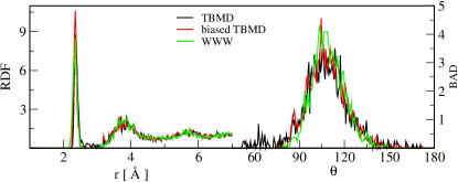
A 216-atom model of liquid silicon (l-Si) was prepared by cooling an initial random configuration from a temperature of 2500 K to the melting point 1780 K in several steps, which were followed by equilibration for a period of 50 ps per step and total-energy relaxations. We have verified that our l-Si model produces features similar to l-Si models obtained from the GSP Hamiltonian by earlier workers Wang et al. (1992); Kim and Lee (1994); Kwon et al. (1994). In figs. 1-2, we present structural and electronic properties from the dynamics for (e.g. conventional MD) and 1 starting with liquid silicon.
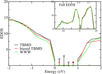
Figure 1 compares the radial and bond-angle distribution functions for three models of a-Si obtained from conventional TBMD, biased TBMD, and the WWW method Djordjević et al. (1995), the last being the “gold standard” of a-Si models. A comparison of the RDFs and an analysis of bond lengths shows that the biased dynamics significantly increases the short-ranged order: the biased model exhibits fewer short and long bonds as compared to conventional TBMD and WWW models. A remarkable feature of the biased-MD model is the absence of 60° bond angles. These angles are typically associated with frozen liquid-like configurations, which plague conventional MD simulations by producing 3-fold defects (dangling bonds). The latter are notoriously difficult to remove from MD models via conventional means and have detrimental effects on electronic and optical properties. It is noteworthy that the inclusion of gap forces can eliminate these unphysical features completely and impart more tetrahedral order in the structure. Atomic coordination is also markedly improved in biased dynamics. Atomic-coordination statistics show that 97.2% atoms in the biased-MD model are 4-fold coordinated. This result is not only superior to 87% 4-fold coordination in conventional MD but also better than earlier works reported in the literature using the GSP Hamiltonian Wang et al. (1992); Kim and Lee (1994); Servalli and Colombo (1993). The biased-TBMD model has fewer defects around the Fermi-energy than the TBMD model (fig. 2). Next, we check these models using using DFT in local density approximation (LDA). LDA calculations with VASP show that the energy of the biased-TBMD configuration is lower than that of the conventional TBMD configurations. Imposing electronic constraints leads to relaxed models in better agreement with structural experiments.
To explore the reproducibility of our method, we sampled 25 well-separated l-Si configurations as starting coordinates and quenched these configurations with as described earlier. This was followed by total-energy relaxations of the models to their respective local minimum. We analyzed these models to obtain the number of atoms with 4-fold coordination as a measure of the merit of the model. Of 25 biased-TBMD models that we studied in this work, 20 models were found to produce better (more tetrahedral) topology than TBMD models.
As a second example we study a-C. Tetrahedral amorphous carbon (ta-C), has some properties reminiscent of diamond while potentially holding some advantagesRobertson (1986); Drabold et al. (1994). The tight-binding model of Xu et al Xu et al. (1992) has been used previously to model ta-C with limited success Wang and Ho (1993). These calculations involved a quench from a high-density liquid (l-C) and volume rescaling at lower temperature. Using the same Hamiltonian, we demonstrate that a simpler melt-quench method can yield improved models. Amorphous carbon dominated by bonding is characterized by a band gap of about 2 eV (depending on the fraction of bonded atoms) in contrast to -bonded a-C, which has a gap of less than 0.5 eV Robertson (1986). The perfectly -bonded WWW model of ta-C Djordjević et al. (1995), relaxed with the Xu Hamiltonian, has a gap of 4.1 eV. We used this spectral range with biased melt-quench TBMD to form models without states in the gap region as exhibited by WWW models.
Starting with liquid carbon of density 3.5 equilibrated at 10000 K, we quenched the model to 700 K at a rate of 500 K/ps. At this point, two parallel runs (quenching) were performed: one with regular TBMD forces () and the other with additional gap forces for . Following first example, we designate these runs as ‘TBMD’ and ‘biased TBMD’, respectively. Both quenched models were relaxed to their respective local minimum until the force on each atom is less than 0.05 eV/Å. Gap forces were switched off during post-quench relaxation for biased-TBMD models. The magnitude of gap forces were found to be smaller () than the corresponding TBMD forces throughout the quenching process.
The unaided TBMD with the Xu Hamiltonian prefers dominated network as observed in our calculations and in Refs. Xu et al. (1992); Wang et al. (1993). The diamond-like -bonded networks reported in Wang and Ho (1993) appear to be an artifact of high density or high pressure on l-C. Our calculations produced models with up to 94% 4-fold coordination compared with 74% and 89% in Wang and Ho (1993). Our results are readily reproducible and do not involve arbitrary manipulation of density. We have conducted 25 quenching runs with different starting liquid models and all of these models produce tetrahedral networks with more than 90% 4-fold coordination.
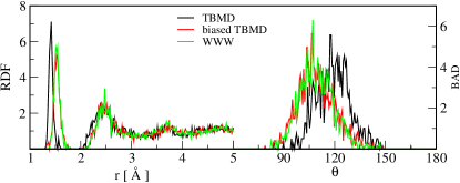
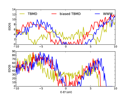
The structural features, including RDF, BDF and atomic coordinations from biased TBMD resemble closely with ta-C WWW model. The TBMD model is dominated by bonding and registers distinct peaks in the RDF and BDF (Figure 3). The density of electronic states of the biased-TBMD model shows that the gap opens up to 0.7 eV as compared to 0.21 eV in the TBMD model. Also, the biased-TBMD model has only 14 states in the gap region exhibited by WWW models as compared to 71 states in the TBMD model: see Fig. 4. The electronic structure of these models is also confirmed by LDA calculations using VASP. The biased-TBMD model shows few scattered states in the gap region as opposed to the ‘metal-like’ electronic structure of the TBMD model. Total energy calculations using LDA show that the biased-TBMD model has 0.31 eV/atom less energy than the regular TBMD model. The biased model is also stable under relaxation using LDA. Such relaxation decreases the total energy by 0.07 eV/atom while preserving structural ordering of the model.
Finally, we have applied this approach to graphene nanoribbons. Using a -point calculation with the same TB Hamiltonian in example 2 on an armchair graphene nano-ribbon (AGNR) of width 11.07 Å, we have carried out low-temperature MD simulations biased toward an enlarged bandgap, without trying to drive the model to a minimum of the total energy. Depending on the value of selected, we obtain structures with gaps of up to 1.58 eV (wider gap is observed using LDA). But these computer models have high strain on the edge atoms and the length of C-C dimers along the edge becomes smaller than the average bond length by 18%.
As we have shown, our method is best employed in a “statistical mode”–unsurprisingly the final structures depend on the initial state. In some fraction () the method does not improve the gap in case of a-Si. We suppose that this may be due to the very simple rule of shifting atoms along gradients toward the nearest band edge, even for eigenvalues very near .
For a-Si, we use a priori knowledge of the gap from the best available models. In the general case, one can define a gap by trial and error, with the choice being determined in part by a requirement that the physical forces vanish at the end. For a-C, considerable flexibility is afforded by our approach in tuning ratios. We have experimented with various , and have found no particular advantage to selecting to date. Furthermore, preliminary studies suggest that the results presented here also accrue for larger (512-atom) models. We expect that the scheme will be useful for many other complex materials not only for discovering structures with desired gaps but also for imposing electronic constraints in modeling.
As is the case with all methods, our approach has limitations: (1) For this first report we use standard tight-binding Hamiltonians for the simulations. Such Hamiltonians are well known to have imperfect transferability (for this reason we are currently extending the scheme to plane-wave DFT, a straightforward but tedious undertaking) and 2) even in a density-functional framework, gap estimates from Kohn-Sham eigenvalues are spurious, though usually these account reasonably well for trends. With significant computational expense, these estimates may be improved e.g. with GW or Hybrid Functional schemes Martin (2004). Despite these limitations, we demonstrate the utility of the method with two examples and suggest that the approach may be developed in promising ways. Nevertheless, it is plain that the method is an extremely useful new tool, even using this simplest implementation.
Acknowledgements.
DAD thanks Army Research Office for supporting this work under Grant W911NF1110358, and Ohio Supercomputer Center. PB acknowledges support from the International Materials Institute for New Functionality in Glass via NSF grant no. DMR-0844014.References
- Liang et al. (2006) J. Liang, E. A. Schiff, S. Guha, B. Yan, and J. Yang, Appl. Phys. Lett. 88, 063512 (2006).
- Kresse and Furthmüller (1996) G. Kresse and J. Furthmüller, PRB 54, 11169 (1996).
- Kresse and Joubert (1999) G. Kresse and D. Joubert, PRB 59, 1758 (1999).
- Martin (2004) R. M. Martin, Electronic structure: basic theory and practical methods (Cambridge university press, 2004).
- Sankey and Niklewski (1989) O. F. Sankey and D. J. Niklewski, PRB 40, 3979 (1989).
- Atta-Fynn et al. (2004) R. Atta-Fynn, P. Biswas, and D. Drabold, PRB 69, 245204 (2004).
- (7) K. Prasai, P. Biswas, and D. Drabold, Unpublished.
- Djordjević et al. (1995) B. R. Djordjević, M. F. Thorpe, and F. Wooten, PRB 52, 5685 (1995).
- Goodwin et al. (1989) L. Goodwin, A. Skinner, and D. Pettifor, EPL 9, 701 (1989).
- Wang et al. (1992) C. Wang, C. Chan, and K. Ho, PRB 45, 12227 (1992).
- Kim and Lee (1994) E. Kim and Y. H. Lee, PRB 49, 1743 (1994).
- Kwon et al. (1994) I. Kwon, R. Biswas, C. Wang, K. Ho, and C. Soukoulis, PRB 49, 7242 (1994).
- Servalli and Colombo (1993) G. Servalli and L. Colombo, EPL 22, 107 (1993).
- Robertson (1986) J. Robertson, Adv. Phys. 35, 317 (1986).
- Drabold et al. (1994) D. Drabold, P. Fedders, and P. Stumm, PRB 49, 16415 (1994).
- Xu et al. (1992) C. Xu, C. Wang, C. Chan, and K. Ho, J. Phys Cond. Matt. 4, 6047 (1992).
- Wang and Ho (1993) C. Wang and K. Ho, PRL 71, 1184 (1993).
- Wang et al. (1993) C. Wang, K. Ho, and C. Chan, PRL 70, 611 (1993).